High Frequency Phase Detector in Phase
Locked Loop
Anto Felix Shaji P
1, R.Mohan Raj*
2Assistant Professor, Dept. of ECE, Jerusalem College of Engineering,Chennai, Tamil Nadu, India1
Assistant Professor, Dept. of ECE, Bharath University, Chennai, Tamil Nadu, India2
* Corresponding Author
ABSTRACT: PHASE-LOCKED loops (PLLs) are widely applied for different purposes in various domains such as
communications and instrumentation. In the microwave range they have been applied in frequency synthesis and phase recovering. In recently years, the evolution of wireless communications has motivated a strong interest towards the development of multi-standards and multi-services with higher operating frequencies using CMOS technology. The phase detector is a key element in PLLs and has from a historical point of view not been able to handle large input frequency differences. The phase detector compares the phase of a periodic input signal against the phase of the output of VCO, and generates an average output voltage Vout, which is linearly proportional to the phase difference, Δφ, between its two inputs. This paper discusses and analyzes various digital phase frequency detector of operating frequency above 2GHz with removal of dead zone. Dead-zone is a small difference in the phase of the inputs that a PFD will not be able to detect. This is due to the delay time of the logic components and rest of the feedback path of the flip flops.
I. PHASE LOCKED LOOP
Phase Locked Loops (PLL) circuits are used for frequency control. They can be configured as frequency multipliers, demodulators, tracking generators or clock recovery circuits. Each of these applications demands different characteristics but they all use the same basic circuit concept. Figure 1 contains a block diagram of a basic PLL frequency multiplier. The operation of this circuit is typical of all phase locked loops. It is basically a feedback control system that control the phase of a voltage controlled oscillator (VCO). The input signal is applied to one input of a phase detector. The other input is connected to the output of a divide by N counter. Normally the frequencies of both signals will be nearly the same. The output of the phase detector is a voltage proportional to the phase difference between the two inputs. This signal is applied to the loop filter. It is the loop filter that determines the dynamic characteristics of the PLL. The filtered signal controls the VCO. Note that the output of the VCO is at a frequency that is N times the input supplied to the frequency reference input. This output signal is sent back to the phase detector via the divide by N counter. Normally the loop filter is designed to match the characteristics required by the application of the PLL. If the PLL is to acquire and track a signal the bandwidth of the loop filter will be greater than if it expects a fixed input frequency. The frequency range which the PLL will accept and lock on is called the capture range. Once the PLL is locked and tracking a signal the range of frequencies that the PLL will follow is called the tracking range.
Generally the tracking range is larger than the capture range. The loop filter also determines how fast the signal frequency can change and still maintain lock. This is the maximum slewing rate. The narrower the loop filters bandwidth the smaller the achievable phase error. This comes at the expense of slower response and reduced capture range.
A. Basic PLL Overview
Phase comparator: As the name implies, this circuit block within the PLL compares the phase of two signals and generates a voltage according to the phase difference between the two signals.
Loop filter: This filter is used to filter the output from the phase comparator in the PLL. It is used to remove
any components of the signals of which the phase is being compared from the VCO line. It also governs many of the characteristics of the loop and its stability.
Voltage controlled oscillator (VCO): The voltage controlled oscillator is the circuit block that generates the
output radio frequency signal. Its frequency can be controlled and swung over the operational frequency band for the loop.
Fig.1 Block diagram of a PLL
B. Phase locked loop operation
The concept of the operation of the PLL is relatively simple, although the mathematical analysis can become more complicated The Voltage Controlled Oscillator, VCO, within the PLL produces a signal which enters the phase detector. Here the phase of the signals from the VCO and the incoming reference signal are compared and a resulting difference or error voltage is produced. This corresponds to the phase difference between the two signals. The error signal from the phase detector in the PLL passes through a low pass filter which governs many of the properties of the loop and removes any high frequency elements on the signal [2-3]. Once through the filter the error signal is applied to the control terminal of the VCO as its tuning voltage. The sense of any change in this voltage is such that it tries to reduce the phase difference and hence the frequency between the two signals. Initially the loop will be out of lock, and the error voltage will pull the frequency of the VCO towards that of the reference, until it cannot reduce the error any further and the loop is locked. When the PLL is in lock a steady state error voltage is produced. By using an amplifier between the phase detector and the VCO, the actual error between the signals can be reduced to very small levels. However some voltage must always be present at the control terminal of the VCO as this is what puts onto the correct frequency. The fact that a steady error voltage is present means that the phase difference between the reference signal and the VCO is not changing. As the phase between these two signals is not changing means that the two signals are on exactly the same frequency [4].
C.Effects of PLL phase noise
PLL phase noise can affect different systems in different ways. However it is important that for all applications the phase noise on the signal is known and within the required limits. However phase noise can give rise to a number of different problems:
Wideband transmitted noise: When PLL frequency synthesizers are used within a transmitter, a local oscillator source with large amounts of phase noise can be radiated away from the wanted frequency band. This is transmitted as wideband noise and can cause interference to other users nearby [5].
bit errors [6]. It is therefore essential that the PLL phase noise is kept to acceptable limits within both the transmitter and receiver.
Reciprocal mixing: This is a problem that occurs when the phase noise from the local oscillator signal is superimposed onto a strong off channel signal. This phase noise then masks out the much lower level weaker signal [7].
D. Types of PLL
Analog or Linear PLL (LPLL): Phase detector is an analog multiplier. Loop filter is active or passive. Uses a Voltage-controlled oscillator (VCO).
Digital PLL (DPLL): An analog PLL with a digital phase detector (such as XOR, edge-trigger JK, phase frequency detector). May have digital divider in the loop.
All digital PLL (ADPLL): Phase detector, filter and oscillator are digital. Uses a numerically controlled oscillator (NCO).
Software PLL (SPLL): Functional blocks are implemented by software rather than specialized hardware.
II. PHASE DETECTOR
A. Phase Frequency Detector
Phase frequency detector is one of the important parts in PLL circuits. PFD (Phase Frequency Detector) is a circuit that measures the phase and frequency difference between two signals, i.e. the signal that comes from the VCO and the reference signal. PFD has two outputs UP and DOWN which are signaled according to the phase and frequency difference of the input signals [10]. Figure 2 shows a PFD with its inputs and outputs.
Fig.2 Phase Frequency Detector
The output signals of the PFD are fed to the charge pump. The output voltage of the charge pump controls the output frequency of the VCO, so with a change happens at the input of the CP the output voltage will change which will change the output frequency of the VCO. In this case the sensitivity of the phase and frequency difference detection of the PFD is very crucial. Sensitivity of the PFD means the smallest difference the PFD can detect and produce UP or DOWN signals that will affect the charge pump, this lead to the conclusion that the higher the sensitivity the better the PFD [8]. One of the disadvantages that PFD suffers is dead-zone.
Fig.3 Detailed PFD and Signals Transaction
From the transaction, once CLKREF goes high it will charge the flip-flop and resulting in changing UP signal to high. when CLKVCO becomes high it will result in changing DOWN signal to high, this will lead to have both output at high which will let the AND gate to signal the reset output and reset both flip-flops driving both outputs to low. Since CLKREF is leading in figure 3(b), we can notice that only UP signal is signaling when CLKREF change to high [11]. In case CLKVCO is leading the opposite is true, which means DOWN signal will be high when CLKVCO change to high.
B. PFD Operation
In simple terms the phase detector is a multiplier. A gain value is also associated with it which we will call, Kv. Let’s start with two sinusoids, S1 (t) and S2 (t). Both have same frequency but are phase shifted by 90°. Now multiply these two signals.
Fg.4 Detecting the phase by multiplying two sinusoids
S2 (t) is cosine hence is 90° shifted from S1(t) S3 (t) = S1 (t).S2 (t)
S1 (t) = A1 sin [ωt + Ф1 (t)] S2 (t) = A2 cos [ωt + Ф2 (t)] Output of multiplier is given by:
S3 (t) = KdA1A2 sin [ωt + Ф1 (t)] cos[ωt + Ф2(t)]
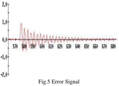
In this form, we see that the multiplier signal consists of two parts one is function of only the phase difference of the two signals, and the second term is at frequency which is twice the signal frequency plus the sum of two phases. When this signal is allowed to pass through low pass filter, only the phase difference term remains at the output and is known as the error signal. And error signal is given by:
Se (t) = sin [Ф1 (t) – Ф2 (t)]
This error signal is then applied to the VCO. As long as the error signal is present, the phase keeps changing linearly, this leads in the change of error signal continuously till error becomes zero.
Fig.5 Error Signal
C. Dead Zone
As we mentioned before, dead-zone is due to small phase error. When the phase difference between PFD’s input signals, the output signals of the PFD will not be proportional to this error. The reason of this problem is the delay time of the internal components of the flip-flop and the reset time that need s the AND gate to reset both flip-flops. Figure 2.5 illustrates the dead zone problem. When the two clocks are very close to each other (small phase error), due to the delay time the reset delay, the output signals UP and DOWN will not be able to charge and no output will signal leading to losing this small difference.
Figure 2.4 illustrates the output voltage of the charge pump vs. the phase error measured by the PDF. Figure 2.4a illustrates the relation in no dead zone PDFs, while figure 2.4b illustrates the relation in the presence of a dead zone. We can see that in a dead zone PFDs the relation become nonlinear around zero. This is due to inability to detect the phase error in this region.
Plenty if solution has been done for this problem some of them reduce the delay time in the internal components of the PFDs, other solution eliminate the reset path by implementing new reset techniques that will not create a delay and produce a high speed PFDs.
Fig. 7 Phase Error vs. Output Voltage (a) No Dead Zone (b) Dead Zone
The existing phase detector consumes high power when operating at high frequency as the internal nodes are not completely pulled up or pulled down. Requires large area for large number of transistors. Limited speed as the maximum operation frequency is inversely proportional to the reset pulse width of the circuit.
III. PHASE DETECTOR ARCHITECTURE
A.Conventional Phase Detector
The basic architecture of a PFD is the conventional PFD as shown in Figure 4. D-FF is implemented using CMOS logic. Inverters can be used for removal of dead zone.
Fig.8 Conventional Phase Detector using D Flip-Flop
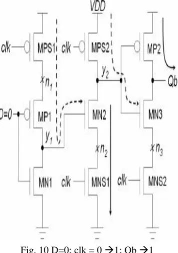
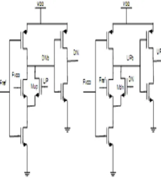
B. Modified pre-charge type PFD
Modified pre-charge type PFD (MPT-PFD) is designed using TSPC-DFF as shown in Figure 5. It has free dead zone using 16 transistors. Of various dynamic CMOS circuit techniques a true single phase clock (TSPSC) dynamic CMOS circuit is operating with one clock signal that is never inverted.
Therefore, no clock skew exists except for the clock delays problem, and even higher frequency can be achieved. The flip-flop consists of 9 transistors, where the clocked switching transistors are placed closer to power/ground for higher speed. The state transition of flip-flop occurs at rising edge of clock.
Fig.9 Modified Pre-Charge Type PFD circuit architecture
Qb become high along clk change from low to high with D = 0. In the figure dotted lines are the conducting paths when clk = 1. I D = 0 and clk = 0, MPS1, MP1, MPS2 are tuned on and node n1, y, and y2 become high. If the signal changes low to high, the node y2 is discharged to low through MN2 and MNS1, making MP2 be on and Qb high. Figure b shows the case with clk changes low to high and D = 1 making Qb low.
Fig. 11 D=1; clk = 0 1; Qb 0
C Falling Edge-PFD
FE-PFD reduces the power consumption of the delay circuit by using a simple architecture composed of 12 transistors. The circuit is free from dead zone.
Fig.12 FE-PFD circuit architecture
In this PFD latch is implemented using domino CMOS NOR gate. There are two latches, the output signal from one latch is fed back to input of other. In one latch, Fref signal act as clock and Fvco and Up signals are acting as input and Dn be input. And in other one Fvco is clock and we get Up as output. The PMOS transistor has width size of 2µm and NMOS has 1µm, both having length of .18nm.
IV. SIMULATION AND ANALYSIS
A. Conventional Phase Detector
Specification • Vref = 1.8V
• Pulse width = 10ns
• Period = 20ns
• Vvco = 1.8V
• Pulse width = 10ns
• Period = 20ns
• Delay = 5ns
• Frequency = 50MHz
• 48 transistor of 0.18μm technology
• Total power at frequency of 50MHz = 33µW • Current through one transistor I = 381.94nA
B. Modified pre-charge type PFD
Specification • Vref = 1.8V
• Period = 2ns • Vvco = 1.8V
• Pulse width = 1ns
• Period = 2ns
• Delay = .5ns
• Frequency = 500MHz
• 16 transistor of 0.18μm technology
• Total power at frequency of 50MHz = 13µW • Current through one transistor I = 347.24nA
C. Falling Edge-PFD
Specification • Vref = 1.8V
• Pulse width = 0.2ns
• Period = 0.4ns
• Vvco = 1.8V
• Pulse width = 0.2ns
• Period = 0.4ns
• Delay = .1ns
• Frequency = 2.5GHz
• 12 transistor of 0.18μm technology
D Analysis
PFD topology
Power Consu mption at 50MHz
No. of
Transist ors used
Max. operatin g Frequen cy
Conventio nal PFD
33µW 48 500MHz
MPT-PFD 13µW 16 1GHz
FE-PFD 6.7µW 12 2.5GHz
A performance comparison between conventional PFD, MPT-PFD, and FE-PFD is shown in Table. FE-PFD is reliable in low power, low jitter, and high speed applications of about 2.5GHz. MPT and FE- PFD are free from dead zone.
V. ADVANCED PFD
The circuit diagram of advanced PFD is as shown in below figure 5.1, it works similar to conventional PFDs but it has many advantages compared to conventional PFDs. This PFD is basically constructed with two GDI (Gate Diffusion Input) cells. A basic GDI cell shown in fig. 5.1 contains four terminals – G (common gate input of nMOS and pMOS transistors), P (the outer diffusion node of pMOS transistor), N (the outer diffusion node of nMOS transistor), and D (common diffusion node of both transistors). This technique allows reducing power consumption, propagation delay, and area of digital circuits. The GDI method is based on the simple cell shown in Figure Table I shows how different logic functions implemented with GDI cell.
Fig.13 Basic GDI cell
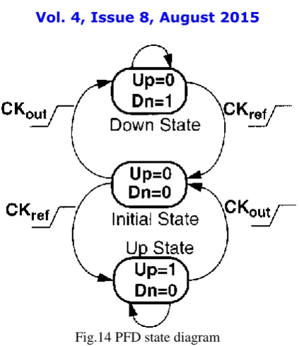
Fig.14 PFD state diagram
At 1.8V voltage supply the maximum operation frequency of the conventional PFD is 500 MHz, for MPt-PFD is 1.5 GHz and the new PFD is 4.5 GHz .
Fig. 15 Circuit diagram of the new PFD
VI. CONCLUSION
This paper provided a performance evaluation of various high frequency phase detector used in phase locked loop (PLL). From the above simulation result it is clear that Modified pre-charge type PFD works in the frequency range of 1 GHz with 16 transistors used. While the Falling Edge-PFD works in 2.5 GHz range with 12 transistors are used for the design. So the power consumption of these phase detector is very less when compared to conventional phase detector. Advanced PFD works in the frequency range of 5 GHz. GDI cell is used as the basic building unit of the phase detector.
REFERENCES
1. Dr. K.B.Khanchandani and Chandan Kumar Akela, “Designing of Phase Frequency Detector for High Speed Applications of Phase Locked Loop (PLL)” in International Journal of Advanced Engineering & Application, Jan 2011, pp. 192-194.
3. Banerjee Dean, PLL Performance, Simulation and Design 4th edition, 2006.
4. Fernando Rangel de Sousa and Bernard Huyart, “A Reconfigurable High-Frequency Phase-Locked Loop” in IEEE transactions on instrumentation and measurement, VOL. 53, NO. 4, Aug 2004
5. Rayen R., Hariharan V.S., Elavazhagan N., Kamalendran N., Varadarajan R., "Dental management of hemophiliac child under general anesthesia", Journal of Indian Society of Pedodontics and Preventive Dentistry, ISSN : 0970-4388, 29(1) (2011) pp.74-79.
6. Cadence Design Environment by Antonio J. Lopez Martin.
7. Shanthi B., Revathy C., Devi A.J.M., Subhashree, "Effect of iron deficiency on glycation of haemoglobin in nondiabetics", Journal of Clinical and Diagnostic Research, ISSN : 0973 - 709X, 7(1) (2013) pp.15-17.
8. Sung-Hyun Yang, Younggap You, Kyoung-Rok Cho, “A new dynamic D flip-flop aiming at glitch and charge sharing free”, IEICE Trans Electron, vol E86-C No.3 March 2003.
9. Sharmila S., Rebecca L.J., Saduzzaman M., "Effect of plant extracts on the treatment of paint industry effluent", International Journal of Pharma and Bio Sciences, ISSN : 0975-6299, 4(3) (2013) pp.B678-B686.
10. S. B. Rashmi, Siva S. Yellampalli, “Design of Phase Frequency Detector and Charge Pump for High Frequency PLL”, IJSCE ISSN: 2231-2307, Volume-2, Issue-2, May 2012.
11. Menon R., Kiran C.M., "Concomitant presentation of alopecia areata in siblings: A rare occurrence", International Journal of Trichology, ISSN : 0974-7753, 4(2) (2012) pp.86-88.
12. B Karthik, TVUK Kumar, Noise Removal Using Mixtures of Projected Gaussian Scale Mixtures, World Applied Sciences Journal, 29(8), pp 1039-1045, 2014.
13. Daimiwal, Nivedita; Sundhararajan, M; Shriram, Revati; , Non Invasive FNIR and FMRI system for Brain Mapping . 14. Daimiwal, Nivedita; Sundhararajan, M; , Functional MRI Study for Eye Blinking and Finger Tapping.
15. Shriram, Revati; Sundhararajan, M; Daimiwal, Nivedita; , Effect of change in intensity of infrared LED on a photoplethysmogramIEEE Communications and Signal Processing (ICCSP), 2014 International Conference on, PP 1064-1067,2014.
16. Kanniga, E; Srikanth, SMK; Sundhararajan, M; , Optimization Solution of Equal Dimension Boxes in Container Loading Problem using a Permutation Block AlgorithmIndian Journal of Science and Technology, V-7, I-S5,PP 22-26, 2014.