ISSN (Print) : 2320 – 3765 ISSN (Online): 2278 – 8875
I
nternational
J
ournal of
A
dvanced
R
esearch in
E
lectrical,
E
lectronics and
I
nstrumentation
E
ngineering
(An ISO 3297: 2007 Certified Organization)
Vol. 5, Issue 3, March 2016
Effect of Varying Parameters on the
Characteristics of Rectangular Patch Antenna
K.Sreelakshmi1 , A.Geethamadhuri2, Ch.Jyothsna3, L.Sreedevi4, G.Umabharathi5
Assistant Professor, Dept. of ECE, GVPCEW, Vishakapatnam, Andhra Pradesh, India1
UG Student, Dept. of ECE, GVPCEW, Vishakapatnam, Andhra Pradesh, India2,3,4,5
ABSTRACT: Microstrip antennas have been one of the most innovative topics in antenna theory and design in recent years, and are increasingly finding application in a wide range of modern microwave systems. This paper focused about the coaxial probe fed rectangular microstrip patch antenna. The input impedance of a microstrip patch antenna is an important design parameter, which controls the radiated power and impedance bandwidth. In the case of a probe fed patch antenna, the total input impedance consists of the probe reactance in series with the patch impedance. This paper presents the design of antenna that operates in S-Band at frequency of 2.4GHz . This paper experimentally investigated the effect on performance characteristics of Rectangular microstrip patch antenna by varying various parameters such as width, height and position of feed. The proposed patch antenna is designed and simulated on HFSS 13.0 software. Ansoft HFSS employs the finite element method, adaptive meshing and brilliant graphics to give you unparalleled performance and insight to all of the 3D EM problems. After the simulation the effect on antenna performance characteristic such as return loss is studied , and 3D and 2D radiation pattern, gain vs frequency plot are obtained.
KEYWORDS: Rectangular microstrip patch antenna, coaxial probe feed,Ansoft HFSS V13,S-Band,Return Loss,Gain.
I. INTRODUCTION
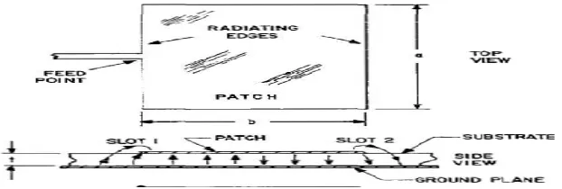
In many applications involving aircraft, and spacecraft, where size and weight. are constraints, low profile antennas may be required.In those applications where bandwidths less than a few percent are acceptable, microstrip antennas may have the desired characteristics [1].These antennas are constructed on a thin ( t << h) dielectric sheet over a ground plane as shown in Fig. 1. The antenna element itself may be square, rectangular, round, etc.,and may have more than one feed point.
Fig.1 Structure of Microstrip Antenna
For a rectangular patch, the length L of the patch is usually 0.3333 λ0 <L < 0.5 λ0, where λ0 is the free-space
ISSN (Print) : 2320 – 3765 ISSN (Online): 2278 – 8875
I
nternational
J
ournal of
A
dvanced
R
esearch in
E
lectrical,
E
lectronics and
I
nstrumentation
E
ngineering
(An ISO 3297: 2007 Certified Organization)
Vol. 5, Issue 3, March 2016
relatively broad beam broadside to the plane of the substrate. Thus the microstrip antenna has a very low profile, and can be fabricated using printed circuit techniques. This implies that the antenna can be made conformable, and potentially at low cost. Other advantages include easy fabrication into linear or planar arrays, and easy integration with microwave integrated circuits..
Disadvantages of the original microstrip antenna configurations include narrow bandwidth, spurious feed radiation,poor polarization purity, limited power capacity,and tolerance problems. Much of the development work in microstrip antennas has thus gone into trying to overcome these problems, in order to satisfy increasingly stringent systems requirements
II. BASIC CHARACTERISTICS OF MICROSTRIP ANTENNAS
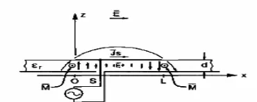
Consider a basic rectangular microstrip antenna with a probe feed, as shown in cross section in Fig. 2(a). When operating in the transmitting mode, the antenna is driven with a voltage between the feed probe and the ground plane. This excites current on the patch, and a vertical electric field between the patch and the ground plane. The dielectric
substrate is usually electrically thin (d < 0.05 λ0), so electric field components parallel to the ground plane must be very small throughout the substrate. The patch element resonates when its length is near λ0 /2, leading to relatively large
current and field amplitudes.
Fig .2(a) Cross section view of Probe-fed patch Fig.2(b)Equivalent circuit of patch antenna
The antenna can be viewed as a cavity with slot-type radiators at x = 0 and x = L, with equivalent magnetic currents,
M= E x n , radiating in the presence of the grounded dielectric substrate. Alternatively, radiation can be considered as
being generated by the induced surface current density, Js= n x H, on the patch element in the presence of the grounded
dielectric substrate. In either case, the equivalent sources produce a broadside radiation pattern .Early analytical models treated the microstrip antenna as a lossy cavity, or as a loaded transmission line resonator [4]-[6].These models involve several simplifying approximations, so they are easy to use and can provide useful information on antenna patterns, impedance, efficiency, and bandwidth. For example, in the cavity model the perimeter of the patch element is approximated as a magnetic wall, for which the electric and magnetic fields of the dominant resonant mode can be expressed as,
vertical electric field = Ez = E0cos(πx/L)
transverse magnetic field = Hy = H0 sin(πx/L)
This result ignores the effect of fringing fields at the edges of the patch, so an ad hoc correction factor must be applied to the patch length to obtain accurate resonant frequencies. An effective dielectric loss tangent is used to account for power lost to radiation. In terms of the transmission line model, the antenna is viewed as a length of open-circuited transmission line with light loading at the ends to account for fringing fields and radiation. The voltage and current on this equivalent transmission line can be approximated as,
Voltage = V(x) = V0cos(πx/L)
Current= I(x)= (V0/Z0)sin(πx/L)
ISSN (Print) : 2320 – 3765 ISSN (Online): 2278 – 8875
I
nternational
J
ournal of
A
dvanced
R
esearch in
E
lectrical,
E
lectronics and
I
nstrumentation
E
ngineering
(An ISO 3297: 2007 Certified Organization)
Vol. 5, Issue 3, March 2016
impedance is a maximum. For a feed point at the center of the patch (x = L/2), the voltage is zero and the current is a maximum, so theinput impedance is zero. Thus the input impedance can be controlled by adjusting the position of the feed point; typical input impedances at an edge of a resonant patch range from1500 to 300Ω. The impedance locus is
that of a half waveopen-ended transmission line resonator, which canbe modeled as a parallel RLC network. Typical equivalent circuit is shown in Fig.2b. The resonant patch element is sometimes made in a different shape (circular being the next most common), but the principles of operation are essentially the same as for the rectangular patch
III . ANALYSIS TECHNIQUES AND COXIAL PROBE FEEDING FOR MICROSTRIP ELEMENTS
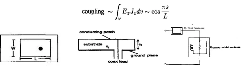
A. Transmission-Line Model
Basically the transmission-line model represents the microstrip antenna by two slots, separated by a low-impedance Zc transmission line of length L
Fig.3 Transmission-line model of rectangular microstrip antenna
Because the dimensions of the patch are finite along the length and width, the fields at the edges of the patch undergo fringing. This is illustrated along the length in Fig. 3 for the two radiating slots of the microstrip antenna. The same applies along the width. The amount of fringing is a function of the dimensions of the patch and the height of the substrate. For the principal E-plane (xy-plane) fringing is a function of the ratio of the length of the patch L to the height h of the substrate (L/h) and the dielectric constant of the substrate. Fringing in this case makes the microstrip line look wider electrically compared to its physical dimensions. Since some of the waves travel in the substrate and some in air, an effective dielectric constant €reff is introduced to account for fringing and the wave propagation in the
line [7].
B.Antenna Design
ISSN (Print) : 2320 – 3765 ISSN (Online): 2278 – 8875
I
nternational
J
ournal of
A
dvanced
R
esearch in
E
lectrical,
E
lectronics and
I
nstrumentation
E
ngineering
(An ISO 3297: 2007 Certified Organization)
Vol. 5, Issue 3, March 2016
Fig 4. Physical and effective lengths of rectangular microstrip patch
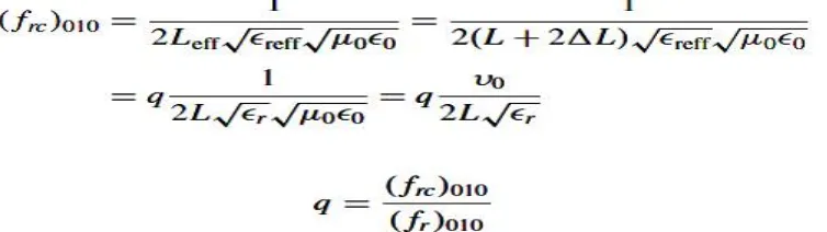
Since the length of the patch has been extended by ∆L on each side, the effective length of the patch is now (L = λ/2 for dominant TM010 mode with no fringing)
For the dominant TM010 mode, the resonant frequency of the microstrip antenna is a function of its length. Usually it is given by
where V0is the speed of light in free space. Since above equation does not account for fringing, it must be modified to
include edge effects and should be computed using
The q factor is referred to as the fringe factor (length reduction factor). As the substrate height increases, fringing also increases and leads to larger separations between the radiating edges and lower resonant frequencies.
C.Coaxial Probe Feeding
Coaxial probe feed consisting of a miniature coaxial connector are widely used for microstrip patch antennas. The feed is located on the axis of the patch and its position from the centre of the patch is adjusted for matching. The feed position for this condition is approximately a third of the way between the patch centre and the edge. The geometry of the patch with a probe feed is shown in Fig. 5a and the antenna equivalent circuit is shown in Fig.5b.Fig 5b shows the equivalent circuit that applies to coaxial probe feed; the parallel RLC network represents the resonant patch, while the series inductor represents feed inductance of the coaxial probe .
ISSN (Print) : 2320 – 3765 ISSN (Online): 2278 – 8875
I
nternational
J
ournal of
A
dvanced
R
esearch in
E
lectrical,
E
lectronics and
I
nstrumentation
E
ngineering
(An ISO 3297: 2007 Certified Organization)
Vol. 5, Issue 3, March 2016
Fig. 5 Basic configuration of probe-fed microstrip antenna a) Geometry b) Equivalent circuit
where L is the resonant length of the patch, and s is the offset of the feed point from the patch edge. This result shows that maximum coupling occurs for a feed at a radiating edge of the patch (s = 0 or L). Such direct contacting coaxial probe feeding method have the advantage of simplicity, but also have several disadvantages. First, these configuration suffer from the bandwidth/feed radiation trade-off discussed above, where an increase in substrate thickness for the purpose of increasing bandwidth leads to an increase in spurious feed radiation, increased surface wave power, and possibly increased feed inductance [9]. For practical purposes such antennas are thus limited in bandwidth to about 2%-5%. Coaxial probes can be used to feed patch elements through the ground plane from a parallel feed substrate , but in an array having thousands of elements such a large number of solder joints makes fabrication difficult and lowers reliability. Finally, although probe feeds primarily excite the dominant mode of the patch element, the inherent asymmetry of these feeds generates some higher-order modes which produce cross-polarized radiation.
IV. PARAMETRIC STUDY OF RMSA
A.Effect of Width
The width W of the RMSA has significant effect on the input impedance,BW, and gain of the antenna.With an increase in W the following effects are observed,the resonance frequency decreases due to the increase in ∆L and €e.The input
impedance at resonance decreases from 180Ω to 36Ω, because the radiation from the radiating edge increases, which decreases the radiation resistance .
B. Effect of height
With an increase in h the following effects are observed. With the increase in h, the fringing fields from the edges increase, which increases the extension in length ∆L and hence the effective length, thereby decreasing the resonance frequency. On the other hand with the increase in h, the W/h ratio reduces, which decreases €e and hence increases the
resonance frequency. However, the effect of the increase in ∆L is dominant over the decrease in €e . Therefore,the net
effect is to decrease the resonance frequency. The input impedance plot moves clockwise due to the increase in the probe inductance of the coaxial feed [10].
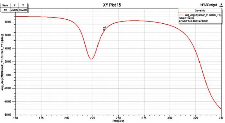
C.Effect of Feed-Point Location
For two different feed-point locations from the center of the patch , the following effects are observed . With an increase in frequency, the input impedance moves in the clockwise direction in the Smith chart. As x increases , the input impedance loci shifts in the right direction on the Smith chart implying that the impedance is increasing .
V .RESULTS AND DISCUSSIONS
A coaxial-fed RMSA of L = 30mm and W = 40mm is considered to study the effects of various parameters on its performance. The probe diameter is taken as 1.6mm for the 50Ω coaxial probe feed using an SMA connector. The
ISSN (Print) : 2320 – 3765 ISSN (Online): 2278 – 8875
I
nternational
J
ournal of
A
dvanced
R
esearch in
E
lectrical,
E
lectronics and
I
nstrumentation
E
ngineering
(An ISO 3297: 2007 Certified Organization)
Vol. 5, Issue 3, March 2016
considering width, height and feed point position as design parameters and by varying this parameters we studied the effect on its performance.The structure of antenna designed using Ansoft HFSS is shown in Fig 6
Fig 6.Ansoft HFSS generated coaxial feed Rectangular Microstrip patch antenna
A.Effect of varying width
Simulations are carried out for the frequency ranges from 1GHz to 3.5GHz and by varying width from 40mm to
50mm.As depicted in Fig 7,the developed patch antenna resonates at a frequency of 2.4GHz with return loss better than -25dB.
(a)
Fig. 7 Return Loss Plot for W = 40mm
ISSN (Print) : 2320 – 3765 ISSN (Online): 2278 – 8875
I
nternational
J
ournal of
A
dvanced
R
esearch in
E
lectrical,
E
lectronics and
I
nstrumentation
E
ngineering
(An ISO 3297: 2007 Certified Organization)
Vol. 5, Issue 3, March 2016
Fig 8.Return Loss Plot for W=50mm
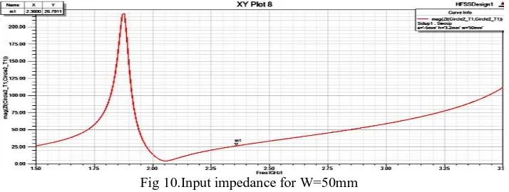
Input impedance is decreased from 39Ω to 27 Ω as shown in Fig 9 & Fig 10.
Fig.9 Input Impedance for W=40mm
Fig 10.Input impedance for W=50mm
B.Effect of varying height
ISSN (Print) : 2320 – 3765 ISSN (Online): 2278 – 8875
I
nternational
J
ournal of
A
dvanced
R
esearch in
E
lectrical,
E
lectronics and
I
nstrumentation
E
ngineering
(An ISO 3297: 2007 Certified Organization)
Vol. 5, Issue 3, March 2016
than -25dB.By varying height from 3.2 to 6.4mm the resonance frequency is decreased from 2.36GHz to 2.26 GHz Fig 7 &11
Fig.11 Return Loss Plot for H= 6.4mm
Input impedance changes from resistance to impedance with inductive reactance shown in Fig 12 & Fig 13.
Fig 12.Magnitude of Input Impedance for H=6.4mm
ISSN (Print) : 2320 – 3765 ISSN (Online): 2278 – 8875
I
nternational
J
ournal of
A
dvanced
R
esearch in
E
lectrical,
E
lectronics and
I
nstrumentation
E
ngineering
(An ISO 3297: 2007 Certified Organization)
Vol. 5, Issue 3, March 2016
C.Effect of varying feed position
Simulations are carried out for the frequency ranges from 1GHz to 3.5GHz and by varying feed position from -5mm to -6mm.As depicted in Fig 7,the developed patch antenna resonates at a frequency of 2.4GHz with return loss better than -25dB.By varying feed position from -5mm to --6mm there is no change in resonance frequency as shown in Fig 14 .
(a)
Fig.14 Return Loss Plot for Feed position = -6mm
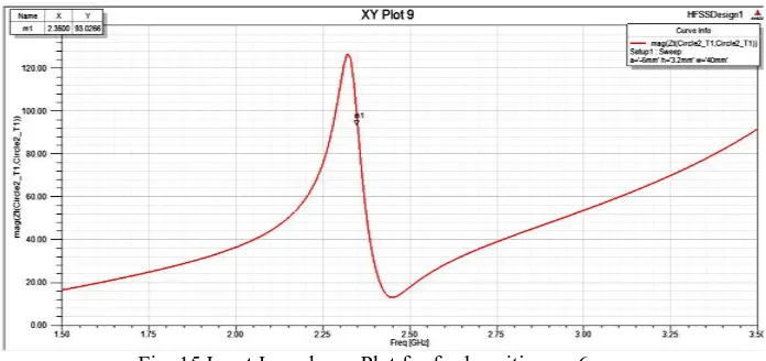
Input impedance increases from 39Ω to 90Ω as shown in Fig 15
Fig .15 Input Impedance Plot for feed position = -6mm
VI.CONCLUSION
ISSN (Print) : 2320 – 3765 ISSN (Online): 2278 – 8875
I
nternational
J
ournal of
A
dvanced
R
esearch in
E
lectrical,
E
lectronics and
I
nstrumentation
E
ngineering
(An ISO 3297: 2007 Certified Organization)
Vol. 5, Issue 3, March 2016
REFERENCES
[1]. Pozar D. M., “Microstrip antennas," Proc. IEEE, Vol.80, No. 1, 79, 91, Jan. 1992.
[2]. J. Q. Howell, “Microstrip antennas,” IEEE Trans. Antennas Propagat.. vol. AP-23, no. 1, pp. 90-93, Jan. 1975.
[3]. K.Sreelakshmi,D.Haripriya,B.Priyanka,”Design Of Aperture Coupled Rectangular Microstrip Patch Antenna to Operate in S-Band at. 2.25Ghz”,International Journal For Scientific Research & Development,Vol 2(12),February 2015
[4]. K. R. Carver and J. W. Mink, “Microstrip antenna technology,” IEEE Trans. Antennas Propag., vol. AP-29, pp. 2-24, Jan. 1981. [5]. R. J. Mailloux, J. F. McIlvenna and N. P. Kemweis, “Microstrip array technology,” IEEE Trans.,Antennas Propagat., vol. AP-29,pp. 25- 37, Jan. 1981
[6]. J. R.James and P. S. Hall, Handbook of Microstrip Antennas. London, U.K.: Peter Peregrinus,1989 [7] . C.A. Balanis, “Antenna Theory, Analysis and Design,”, 2nd Ed., John Wiley & sons, inc., New York.
[8]. B.M.Alarjani and J.S.Dahele.”Feed Reactance of Rectangular microstrip patch antenna with probe Feed” ,Electronic Letters ,vol 36(5),pp. 388-390 ,March 2000
[9] . D. H. Schaubert, D. M. Pozar and A. Adrian, “Effect of microstrip antenna substrate thickness and permittivity: Comparison of theories and experiment,” IEEE Trans. Antennas Propagat., vol. 37, pp. 677-682, June 1989.