83
32-Bit Linear Feedback Shift Register With Power
Gating Technique
Rebecca Angela Fernandes
M. Tech Student, Dept. of E&C EngineeringN.M.A.M. Institute of Technology Nitte, India
E-mail: [email protected]
Niju Rajan
Assistant Professor, Dept. of E&C Engineering N.M.A.M. Institute of Technology
Nitte, India
E-mail: [email protected]
Abstract - In the VLSI design flow testing of the design plays a major role as any VLSI circuit consumes more
power in the testing mode compared to the functional mode. Static power dissipation is caused by leakage current and it is very small in VLSI circuits. In the idle mode when the circuit is not performing any operation power gating has proved to be efficient in reducing the leakage power dissipation. The main objective of power gating is to reduce the leakage power dissipation by adding sleep transistors and shutting off the idle blocks of the circuit. The sleep transistor can act as a footer switch or as a header switch depending on where the sleep transistor is added in the circuit. The sleep transistor is called footer switch if an NMOS transistor is added between the virtual ground rail and actual ground rail and it is called a header switch if a PMOS transistor is added between the virtual source rail and actual source rail. In this paper a traditional 32- Linear Feedback Shift Register (LFSR) without power gating is implemented and the leakage power report is then compared with LFSR designed using different power gating techniques.
Keywords—Leakage power dissipation, Linear Feedback Shift Register (LFSR), Power gating, Fine Grain
Power Gating (FGPG), Coarse Grain Power Gating (CGPG).
I. INTRODUCTION
Testing of the system is done to avoid the defective component in the system rather than replace the component later. Once circuit is designed, it is important to test the circuit for their proper function and usability. Components within the Integrated Circuit (IC) is increased based on the need of the user, so testing of the component requires powerful testing methods to check the proper function and usability of the components. Static and dynamic power dissipations are the two major issues for the power consumption during test. Leakage current contributes to static power dissipation and it is very small in VLSI circuits. Leakage power is a major concern in CMOS technologies and numerous design techniques have been introduced to reduce stand-by leakage in digital circuits. Power Gating techniques have proved to be efficient in reducing the leakage power.
[1], proposed that the power dissipation in the testing mode is greater than the normal mode. The scheduling process provides optimization for power dissipation in addition to other common constraints. The control architecture, on the other hand, provides an autonomous BIST activation and a diagnostic capability to identify failed blocks. [2], explained about two types of testing, external testing and internal testing. External testing uses
ATE which includes input pattern generator, testing circuit and decision circuit. Using external circuit, input patterns are generated, which is given to the IC fixed in testing circuit, the output of this is given to the decision circuit, then it is compared with the stored correct output to test the correctness of the circuit. If the output is not matched with the stored correct output then it is rejected. So the external testing takes more time compared to internal testing. In internal testing, test time is greatly reduced by maintaining the test circuit inside the IC along with the testing components. These type of Transistor is obtained. The results have shown that power gating using sleep transistor had reduced the leakage power.”[4], explained the benefits and cost of power gating technique. They have considered a standard chip and a power-gated chip both implementing the same functionality. In the standard chip, all logic circuits are connected to
through a hierarchical power mesh. The entire
84 the local mesh to the global mesh. Their results
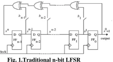
show that power-gating has proved to be very efficient in reducing the stand-by leakage currents in the idle mode.”[5], explained the important and vital parameters such as sizing of sleep transistor, mode transition energy, reduction of noise, area, delay and noise margin that need to be considered while using the power gating technique.”[6], presented the different techniques of power gating. The techniques are as follows: 1) Fine Grain Power Gating (FGPG) and 2) Coarse Grain Power Gating (CGPG). pseudorandom pattern generators to generate a random number of 1s and 0s. There are two types of LFSR-external feedback LFSR and internal feedback LFSR. In external feedback LFSR, the XOR gate is placed in the feedback path whereas in internal feedback LFSR, the XOR gate is placed between adjacent D flip-flops.The maximum-length of an LFSR sequence is 2n-1.
Fig. 1.Traditional n-bit LFSR
III. POWER GATING
In the integrated circuit design in order to reduce the leakage power consumption the power gating technique is used. Power gating technique makes use of a sleep transistor. The leakage power is reduced by turning-off the sleep transistor when the circuit is in idle mode and turning-on the sleep transistor when the circuit is in functional mode. The input to the sleep transistor can be given through an internal gate or by an external source. Sleep input through an external source is preferred for large circuits as it causes less switching and hence not much increase in dynamic power dissipation. One of the major parameter to be considered in power gating technique is the power gate size. A header PMOS transistor or footer NMOS transistor can be chosen by the designer
depending on the circuit. Usually a footer switch is preferred as it is smaller in area for the same switching current. There are two types of power gating techniques: 1) Fine Grain Power Gating (FGPG) 2) Coarse Grain Power Gating (CGPG).
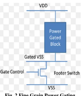
A. Fine Grain Power Gating (FGPG)
85
Fig. 2.Fine Grain Power Gating
B. Coarse Grain Power Gating (CGPG)
In this power gating technique a sleep transistor is inserted between a cluster of cells that are used to design the VLSI circuit as shown in Fig. 3. This technique uses the grid style of sleep transistors where the cell is driven through shared
virtual ground network. In this paper the basic 2-bit NAND gates and 3-bit NAND gates that are used to design the D flip-flop using power gating technique is implemented by inserting one NMOS footer sleep transistor between the actual and virtual ground rail of all the basic circuits.
Fig. 3.Coarse Grain Power Gating
IV. IMPLEMENTATION
D flip-flop and Linear Feedback Shift Register (LFSR) circuits are designed using Cadence Virtuoso tool with 90nm CMOS technology. The transient analysis is done by launching ADEL for verification of schematic results. The power report is obtained for D flip-flop
and 32-bit Linear Feedback Shift Register (LFSR) with and without using power gating technique. A. D flip-flop
86
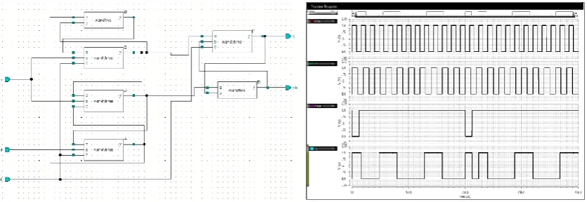
Fig. 4.Schematic of 2-input NAND gate Fig. 5.Schematic of 3-input NAND gate
Fig. 6 shows the schematic of D flip-flop without using power gating and Fig. 7 shows the transient response of D flip-flop which is obtained by launching ADEL.
Fig. 6.Schematic of D flip-flop Fig. 7.Transient response of D flip-flop
Fig. 8 and Fig. 9 shows the schematic of 2-bit NAND gate and 3-bit NAND gate with one sleep transistor inserted in each NAND circuit respectively. These circuits are used to design the D flip-flop with Fine Grain Power Gating (FGPG).
87 Fig. 10 shows the schematic of D flip-flop using Fine Grain Power Gating (FGPG), where one sleep transistor (NMOS) is inserted between the virtual and actual ground rail of each NAND gate and Fig. 11 shows the transient response of D flip-flop which is obtained by launching ADEL.
Fig. 10.Schematic of D flip-flop with FGPG Fig. 11.Transient response of D flip-flop with FGPG
Fig. 12 and Fig. 13 shows the schematic of 2-bit NAND gate and 3-bit NAND gate, where only one sleep transistor needs to be inserted between all the NAND circuits used to design the D flip-flop. These circuits are used to design the D flip-flop with Coarse Grain Power Gating (CGPG).
Fig. 12.Schematic of 2-input NAND gate with CGPG Fig. 13.Schematic of 3-input NAND gate with CGPG
Fig. 14 shows the schematic of D flip-flop using Coarse Grain Power Gating (CGPG), where one sleep transistor (NMOS) is inserted between the
88
Fig. 14.Schematic of D flip-flop with CGPGFig. 15.Transient response of D flip-flop with CGPG
B. 32-bit Linear Feedback Shift Register
(LFSR)
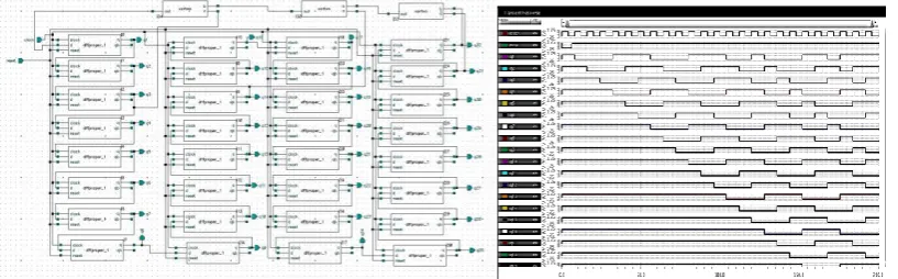
The 32-bit LFSR is designed for the polynomial 𝑥32 + 𝑥31 + 𝑥14 + 𝑥3 + 1. Fig. 16 shows
the schematic for 32-bit LFSR designed using D
flip-flops without using power gating as shown in Fig. 6 and XOR gates. Fig. 17 shows the transient response of 32-bit LFSR.
Fig. 16.Schematic of 32-bit LFSRFig. 17.Transient response of 32-bit LFSR
Fig. 18 shows the schematic for 32-bit LFSR with Fine Grain Power Gating (FGPG) technique, where the 32-bit LFSR is designed using power gated D
flip-flops as shown in Fig. 10 and XOR gates. Fig. 19 shows the transient response of 32-bit LFSR using FGPG.
Fig. 18.Schematic of 32-bit LFSR with FGPG Fig. 19.Transient response of 32-bit LFSR with FGPG
Fig. 20 shows the schematic for 32-bit LFSR with Coarse Grain Power Gating (CGPG) technique, where the 32-bit LFSR is designed using power
89
Fig. 20.Schematic of 32-bit LFSR with CGPG Fig. 21.Transient response of 32-bit LFSR with CGPG
V. POWER ANALYSIS
The power report is calculated using Cadence tool calculator.
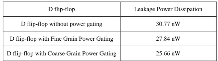
Table 1: Power Analysis of D flip-flop
D flip-flop Leakage Power Dissipation
D flip-flop without power gating 30.77 nW
D flip-flop with Fine Grain Power Gating 27.84 nW
D flip-flop with Coarse Grain Power Gating 25.66 nW
Table 1 shows the leakage power of a normal D flip-flop and also power gated D flip-flop’s with Fine Grain Power Gating (FGPG) and Coarse Grain Power Gating (CGPG) techniques. There is 9.52% leakage power reduction in D flip-flop
implemented using Fine Grain Power Gating (FGPG) technique and 16.60% leakage power reduction in D flip-flop implemented using Coarse Grain Power Gating (CGPG) technique compared to the normal D flip-flop.
Table 2: Power Analysis of 32-bit LFSR
32-bit LFSR Leakage Power Dissipation 32-bit LFSR without power gating 1806.4 nW
32-bit LFSR with Fine Grain Power Gating 1566.6 nW 32-bit LFSR with Coarse Grain Power Gating 1301.3 nW
Table 2 shows the leakage power of a normal 32-implemented using Fine Grain Power Gating (FGPG) technique and 27.96% leakage power reduction in 32-bit LFSR implemented using Coarse Grain Power Gating (CGPG) technique compared to the normal 32-bit LFSR.
VI. CONCLUSION
The 32-bit Linear Feedback Shift Register (LFSR) has been designed for the polynomial 𝑥32 +
𝑥31 + 𝑥14 + 𝑥3 + 1.The D-flip flop, XOR gates and
LFSR were designed using Cadence Virtuoso tool. The leakage power of normal D flip-flop and 32-bit LFSR has been compared with the power gated D flip-flop and 32-bit LFSR, it is observed that there is leakage power reduction in the power gated circuits when compared to the normal circuits.
REFERENCES
[1] Zorian Y., “A Distributed BIST Control Scheme for Complex VLSI Devices”, IEEE CS Press, Los Alamitos, Calif., 1993, pp 4-9. [2] Abromovici M., Breuer M.A., Friedman,“Digital Systems Testing and Testable Design”, NJ: IEEE Press, 990, pp. 182-196, pp. 457-468, and pp 477-481. [3] C. ChrisjinGnanaSuji, S. Maragatharaj and
R.Hemima, “Performance Analysis of Power Gating designs in Low Power VLSI Circuits”, International Conference on Signal Processing, Communication, Computing and Networking Technologies, 2011.
[4] Hailin Jiang, Malgorzata Marek-Sadowska, and Sani R. Nassif, “Benefits and cost of Power Gating”, International Conference on Computer Design, 2005.
90 [6] Akhila Abba and K Amarender, “Improved
Power Gating Technique for Leakage Power Reduction”, International Journal Of Engineering And Science, Volume 4, Issue 10, October 2014, pp 06-10.
[7] Madhushree K. and NijuRajan, “Dynamic Power Optimization of LFSR Using Clock Gating”, International Conference on Innovations in Information, Embedded and Communication Systems (ICIIECS), Volume 5, pp. 429-432, 2017.