Design and Enactment of FIR Filter Utilising
Precise CSE and Probable GB Algorithm
Vijesh Vijay, Prof. Hussain Ahmed
Department of Electronics and Communication Engineering, HKBK College of Engineering, Bangalore, India
Professor & HOD, Department of Electronics and Communication Engineering, HKBK College of Engineering,
Bangalore, India
ABSTRACT: Finite impulse response filters has become more of prominance nowadays. In the suggested work, we premeditated with the CSE and GB algorithm which are followed with the Boolean network. There is lucid formalisation of the 0-1 problem of LP. Different modus operandi worked with an algorithm to bring forth the power in consumption to nadir at possible and for an augmented efficiency with headway of project.
I. INTRODUCTION
Finite impulse response filters are gaining prominence these days in digital signal processing and DSP systems fundamentally since their characteristics are in unswerving phase and even feed forward with those of enactments, which makes them very useful building the firm high rendition at filters[1]. The direct and those of transposed form of the respective FIR filter in enactments worked respectively. Both the architectures are at semblance in those of labyrinthine in hardware as well as transposed form, which is defacto preferable because of its higher rendition and even effeciency at power.[2]
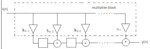
The multiplier block of the respective digital filter of FIR, in transform, with complexity and those of rendition of the respective design, since a gigantic number of constant multiplications being even becoming an essential. This is known as the multiple constant in multiplicaions that is, with MCM operations and it is the main operation and performance of the bottle neck in many of the other DSP systems as agile than the Fourier transforms discrete cosine and codes in relevance to rectifying the errors.
Altough here area, delay and power efficient multiplier in architectures which comprises of Wallace and those of amended Booth multiplers has been suggested and absolute flexibility of the respective multiplier is not defacto necessary for the unfluctuating multiplications since their filter coeffients are fixed and even determined beforehand by the DSP algorithms.[3]-[4]
II. SUGGESTED WORK
Precise CSE Algorithm
The exact CSE algorithms comprises of four of the main steps. First, all the possible enactments of the constants are defacto extracted from the non-void digits constants, which is defined under those a number in representation: Binary, CSD or of MSD.
Partial Terms
In the respective pre-processing phase, the constants are to be muliplied by a known variable, which are converted to those of positive, and then made odd by the successive divisions, that is by two. The constants in results are reserved without any repetition in the respective target set T. Thus, T comprises the minimum number of necessary constants which are to be enacted. The part of that algorithm, w the enactments of the respective target in constants and those partial terms are actually found as follows.
Take particular elements from T, make out the relevant representations, and reserve them in a set or group, which can be identified as S. Form of an empty set that is O, which is concorded with those of t, which comprises of the inputs and respective amount of left shifts , of all the addition or subtraction operations, which are actually generated the ti .
For each of those representations of which ti in the respective set that is S
Gestimate all of the non symmetric in partial in term pairs that is representing i.
In each of the pair, make each of the partial term being positive and covering those of representation of ti odd, and those determining its respective amount of left shift.
Add each of the pair to the respective set O with those of amount of respective left shifts of partial terms i.
Add each of the partial term in T, if it does not actually represent the respective input which the constant are considered in multiplication with, which is denoted by one and is not in those of T.
Recapulate step one until all the respective elements of T are considered. Observe that the particular target set as T only comprising the target constants and which need to be enacted in stage of commencement of the respective iterative loop, and in the later iterations and it is augmented with the partial terms, which are required for the respective enactments of the target constants.
As an instance, we consider twenty five as a target constant, which is expressed under MSD, and which has two of the representations that is 011001 and even 10 1001 respectively.
Structuring of the Boolean Network
At the post of possible enactments of the target constants and the partial terms are found and they are represented in a chosen network which comprises of only AND and OR gates. Its properties are given as follows.
The primary input of the respective network is the input variable, which is to be multiplied with those of constants.
An AND gate in the respective network which represents an addition or subtraction operation can be constituted with two inputs.
An OR gate in the respective network actually represents a target constant or a partial terms which amalgamates all of its possible enactments.
Fig.1. Network structured for the target constant 25 under MSD.
The Boolean network is developed as follows.
Considering an element from T,t
For these each of the respective pair in Oii, generates a two-input AND gate. The input of those AND gate are actually the elements of the respective pair, that is one, denoting the respective input, that the actual constants, which are multiplied with or those of outputs of OR gates, which are representing the target constants or the partial terms in the respective network.
Generate an OR gate which is associated with t, w the inputs are the turnouts of the resepctive AND gates, which are determined in the step two.
If tii is a particular targer constant, makes the respective output of the corresponding OR gate making to an output of the respective network.
Repeat the step one until and unless all the elements are in T are considered.
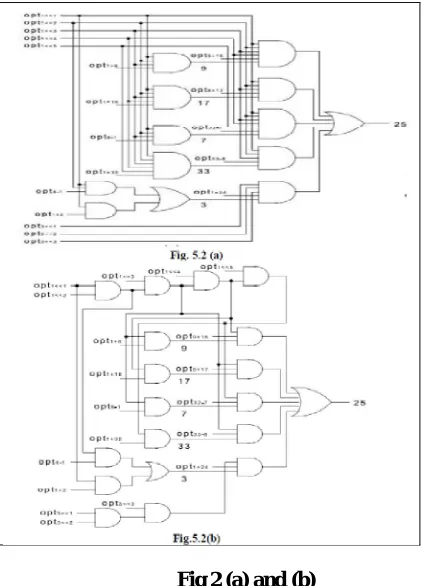
The particular network generated for the target constant is twenty five defined as under the MSD is given , where one-input OR gates for the partial terms seven, nine, seventeen and thirty three are annhilated and the of the respective operations are shown inside each of the respective AND gate.
III. FORMALISATION OF THE 0-ILP PROBLEM
To make to comprisal of the optimisation of variables into the respective network. , we can conveniently lead to a formalisation of the gate level in area at optimisation as a zero-one ILP problem. The variables of optimisation are concorded with those of two parameters, which has different enactments in cost at the gate level, that is to addition or subtraction operations and left shifts of the respective constants partial terms and target constants.
For each of AND gate which represents an addition or subtraction operation respective in the network and we commence an variable of optimisation, which are associated with the operation, which can be recognised opt where a and those of b signifies the input of the respective operation and we consider summing this particular variable to those of input of the respective AND gate.
In order to go for maximisation, the sharing of the left shifts that is the D flip and flops at the respective gate level for each of the constant c as in the figure, considered network which is structured for the respective target in constant twenty five under those of MSD. Then, for each of the constant c with mls c, which is greater than zero, we introduce mls optimisation, which are variables that is representing left shifts of C from one to mls c that is opt C_1, opt C_2.
In the cost function, w it has to be actually minimised, the cost value of this of optimisation in variable, which is actually determined as the gate level and cost of one D being flip and flop. The inclusion of that optimisation of the variables into the network can be performed in two of the ways.
Model one: for each of AND gate in the respective network which are representing an addition or subtraction in operation, if an input signal ins and is relocated by 1s which is greater than the void times, then we herien include 1s in additional inputs standing for the optimisation variables, which are defacto associated with the 1s left shift of the respective signal ins that opt ins being logical shift to one, opt ins is logical shift to opt and is logical shift to 1s.
Fig 2 (a) and (b)
Networks constructed for the target constant twenty five MSD after the optimisation variables which are added (a) under model one (b) under model two.
Then, for each AND gate representing an addition or subtraction operation, if the respective input signal ins is shifted by ls which is greater than zero times, we add the signal input to the respective AND gate. The input of the variable x is denoted by one, which can be eradicated from the inputs of the AND gates, because of logic value and which is greater than one and it is considered available.
Figure 2(a) and (b) which illustrates the respective networks are generated for the target constant that is twenty five under the MSD at the post unravelment which are performed and the variables of optimisation are added under the respective Models 1 and 2 respectively. At the post optimisation, variables are actually added into the respective network, the zero-one ILP problem, which is generated .
The respective constriants of the zero- one ILP problem are procured by finding the respective CNF formulas of each of the gate in the respective network and expressing each of the clauses of the respective CNF formulas as a beeline inequality. The output of the respective network that is output of the OR gates are to be associated with the target constants, which are set to one.
Observing at figure 2 (a) and (b) that of model one generates as 0 to one ILP gates which are utilised in the model two. However, the zero-one ILP problem constructed under model two has significant less number of those constraints than those of the model one since the number of respective inputs of an AND gate representing an addition or subtraction operation, which is increasing only by one during the comprising of those optimisation variables, which are denoting the left shift of a constant respectively in model 2. Note that the respective number of optimisation variables, which are under the both models are actually the same.
IV. APPROXIMATE GB ALGORITHM
Optimisation of the gate level area are problem in the digit serial MCM design and it is actually an NP complete problem which is due to NP absoluteness of the respective problem of MCM. Thus naturally, there will be always zero-one ILP problems, that are regulated by the exact algorithm of CSE and which the current zero-one ILP solvers find much problematic to handle.
GB heurisitic algorithms, which come with a good solution utilising less of the computional resources are actually indispensable. In our approximate algorithm it is called the MINAS-DS w it is done in the algorithms and are designed for the MCM problem, are expressed in the definition one, we heren find the fewest of the number of those intermediate constants, which includes all the target and those of intermediate constants that are synthesised utilising a single operation.
However, chosing all the intermediate constant for those of enactments of not yet of synthesised target constants in each of the redundancy, we favor those of among possible intermediate constants, which are to be synthesised utilising the least of the hardware and it will enabled to enact those of not yet considered synthesized target constants in a smaller area with those of available constants.
V. ENACTMENTS
1) FIR filter
FIR filter in realisation as according to those of hardware and even software in frequency in response must be be in time makes domain format. To find the respective domain output, which the sample z transform was utilised and those of computed utilising (2) is described below.
In those of formula x of n-k denotes the sample input which is delayed by those of factor n. h[k] is actually the coefficient of those FIR filter and y of n is the filter sample output.
As FIR is less sensitive than the infinite impulse response to bring a constant accuracy for same order. FIR is enacted in several of the realisation formats. Only of the direct and optimised formats were actually utilised for software enactments of purpose due to its convenience over other in realisations.
It results into a stable filter in digital world with those of high rendition. FIR filter in enactment is actually exhibited below in the figure 3.
Figure 3: FIR filter in enactment
We consider the enactment of those transposed, in the form of FIR filter with the generic multipliers. The multiplier block of the respective digital FIR filter in its transposed form, where those of multiplication of filter coeffiecients with the filter input is realised and has significant impact at the entanglement and the rendition of the respective design because of a large number of constant multiplications are necessitous. , we accumulate all the multiplication in operation together and it is named as the multiplier block as in the figure expressed below.
Fig. 4. Multiplier block that accumulates all of the multiplication operation together
2) CSA
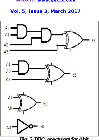
Fig. 5. BEC enactment for 4 bit.
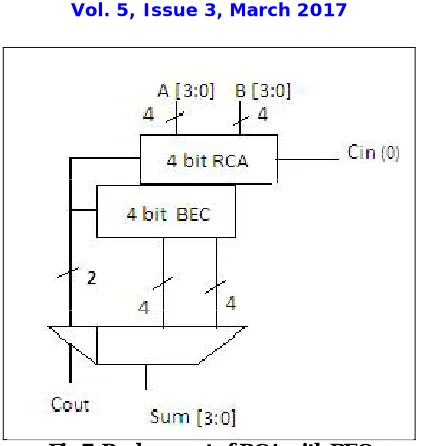
To make replace one of RCA, the circuit with BEC, first of need has to be enacted or uncomplexed the CSA utilising two of RCA. This exhibits as in figure four.
Fig. 6. Enactment of CSA with two RCA
In the above circuit, it is to eliminate the disadvantages of the respective RCA and make those of circuit according to the specification which are actually described in the whole of paper.
Fig 7. Replacement of RCA with BEC
VI. RESULTS
In this particular paper, focus is mainly on the lessening of the respective power in consumption and any delay along the reduction in the area. In this, the BEC method is utilised to uncomplex those of addition as well as the at the GB method. Particularly, in this BEC procedure is utilised for uncomplexing the addition that is as well as those of GB method. It produces the great turnouts utilising less of the computation resources. BEC method is enacted in the respective Verilog coding and an executed utilising the Xilinx software. The below considered table exhibits the difference between the two of the respective techniques CSE and GB for those of four tap and eight tap FIR filter
FOUR TAP FIR FILTERS
Table 1: Comparison of 4 tap FIR
Consumption
of Power
(W)
Frequency
in
Maximum
(MHz)
Delay
(ns)
No: of
Slice
Registers No:
of
LUTs
CSE_CSA 0.234 336.134 31.055 92 418
CSE_CSA_BEC 0.217 396.118 3.399 90 310
GB_CSA 0.210 336.134 30.530 92 407
EIGHT TAP FIR FILTERS
Table 2 Comparison of 8 -tap FIR Filters
VII. CONCLUSION
FIR filter is significant part of the respective DSP system and it is widely utilised to enact any of VLSI and the respective communication circuits. In this particular project we utilised both of CSE and GB modus operandi along with those of CSA which utilises amalgam of RCA and those of BEC to compare the respective results. By utilising the amalgam, the respective areas will reduce and it will results in better efficiency and those of consumption of power can be ascertained. Both of the four tap and eight tap filters are designed and it is compared with the respective delay, consumption of power and the area premeditated along. When considering gestimation of two of the four tap and eight s tap of filters, precision are found more of at eight tap filters. Powers in devouring are almost of the same for the both filters but any lagging for more of the eight tap in filters can be ascertained.
REFERENCES
[1]. Jeong .W and Roy .K, “Robust high-performance low power adder”, Proc. of the Asia and South Pacific Design Automation Conference, pp. 503-506, 2003.
[2]. Anitha Kumari R D, Nayana N D, “Low power and Area Efficient Carry Select Adder”, National Conference on Electronics, Communication and Signal Processing, NCECS-2011.
[3]. He Y, Chang C H, and Gu J, “An area efficient 64-bit square root carry select adder for low power applications,” in Proc. IEEE Int. Symp. Circuits Syst., 2005, vol. 4, pp. 4082–4085.
[4]. Hosseinghadiry M, Mohammadi H and Nadisenejani M, '' Two New Low Power High Performance Full Adders with Minimum Gates", World Academy of Science, Engineering and Technology 52 2009.
[5]. Ceiang T Y and Hsiao M J, “Carry-select adder using single ripple carry adder,” Electron. Lett., vol. 34, no. 22, pp. 2101–2103, Oct. 1998. [6]. Bedrij O.J, “Carry-select adder,” IRE Trans. Electron. Comput., pp.340–344, 1962.
Consumption of power (W)
Frequency being Maximum (MHz)
Delay (ns)
No: of Slice Registers
No: of LUTs
CSE_CSA 0.294 304.674 35.391 210 1285
CSE_CSA_BEC 0.235 305.343 5.056 196 973
GB_CSA 0.287 309.387 35.146 202 1022