ISSN(Online): 2320-9801
ISSN (Print) : 2320-9798
I
nternational
J
ournal of
I
nnovative
R
esearch in
C
omputer
and
C
ommunication
E
ngineering
(An ISO 3297: 2007 Certified Organization)
Vol. 3, Issue 9, September 2015
PCB Defect Detection and Classification by
Image Erosion Technique
AR.Arunachalam
Assistant Professor, Department of Computer Science, Bharath University, Chennai, Tamil Nadu, India
ABSTRACT: A technique of PCB layout optical inspection based on image comparison and mathematical erosion methods is proposed. The unique feature of the technique is that the inspection is performed at different stages of image processing. The presence of all layout elements is checked up, then positions of found elements and their conformity to project rules are verified, the breakouts and shorts are found. The inspection of mouse bits, spur and pinholes on conductors is also carried out.
I. INTRODUCTION
An important problem in manufacture of a microelectronic equipment is the printed circuit board (pcb) layout inspection. The non-contact optical methods is widely used the control of pcbs.
An object for the inspection will be the image of pcb layout. The problem definition is the following. The raster pattern of the pcb layout and the set of project rules are given. The artwork image of pcb layout can be given in addition. It is required to check whether the pcb elements meet the given project rules, and to described their defects.
As elements on the pcb layout image we will define the contact pads, conductors, control points and the service information in the character form. The defect under inspection is the deviation of layout elements on pcb layout image from the project documentation owing to errors by manufacture, such as discrepancy of temperature and manufacture time modes, mechanical misregistration, etc. The example of some defects is replaced on fig.1. The defects can be divided into the following kinds: spurious copper (1), spur (2), mousebit (3), pin hole (4), short (5), breakout (6), discrepancy of the conductor minimal width and the minimal distance between conductors to project rules, absence or displacement of any element [1].
ISSN(Online): 2320-9801
ISSN (Print) : 2320-9798
I
nternational
J
ournal of
I
nnovative
R
esearch in
C
omputer
and
C
ommunication
E
ngineering
(An ISO 3297: 2007 Certified Organization)
Vol. 3, Issue 9, September 2015
II. DESCRIPTION OF THE TECHNIQUE OF PCB LAYOUT INSPECTION
Preliminary image processing
Preliminary processing of the test image consists of binarization, corrections of a rotation angle and scaling. The gray-scale picture received from an optical system is transformed to a binary image using the treshold Bts calculeted by the formula:
Bts = 2/3 * (Bmax - Bmin), (1)
where Bmax and Bmin are the maximal and minimal values of brightness of the image.
The test image can have distortions of scale and a rotation angle. Control points are used To correct these distortions. The control points are selected on the reference image, and then the search of these points is performed on the test image. Finally the correction of the rotation angle and scale is carried out[5].
Search of all contact pads is made on the binary image, and lists of contact pads for the reference and test image are formed accordingly. The reference and test lists are compared with each other, therefore presence of all elements on the PCB layout image is checked up, and finally verification of found elements position is performed[6].
. The PCB layout inspection
After the preliminary processing the search of defects by a method of pixel by pixel calculations of XOR logic operation on reference and test images is carried out. It is necessary to carry out the following tasks:
1. Find faults of the PCB by comparison a binary reference and test images.
2. Measure geometrical parameters of defect are: length, height and the area[1].
3. Classify faults as:
spurious copper;
spur;
mousebit;
pin hole;
short;
breakout
III. THE INSPECTION ON THE VECTOR IMAGE OF PCB LAYOUT
Search of faults like spur and mousebit on vector representation of the image of the PCB is realized on the basis of algorithms Weiler-Atherton and Margalit-Knott. For search of faults vector representations of reference and test images of PCB are used[7].
ISSN(Online): 2320-9801
ISSN (Print) : 2320-9798
I
nternational
J
ournal of
I
nnovative
R
esearch in
C
omputer
and
C
ommunication
E
ngineering
(An ISO 3297: 2007 Certified Organization)
Vol. 3, Issue 9, September 2015
pixels[13]-[14]. Pixels of defect have black color and are marked by small white squares. Pixels which border on defect, are marked by diagonal lines. It can be seen that:
defect looks like a set of black pixels on a white background;
defect is adjoined with both black and white pixels of the image;
defect adjoins only to one element on the image (element 1).
According to table 1 the defect is classified as spur.
For faults like spur and mouse bit the additional check is made: if the fault borders on two or more PCB elements on initial images, it belong to the class of short and breakout accordingly[15][16].
V. THE INSPECTION THE MINIMAL CONDUCTOR WIDTH AND THE MINIMAL
DISTANCE BETWEEN CONDUCTORS
At the certain PCB manufacturing phase there is a necessity to check conformity of the minimal width of a conductor and the minimal distance between conductors to project rules. Localization of points on the image, where these project rules do not carry out, is made with use of mathematical erosion operators “OPEN” and “CLOSE” [17]. To define conductor regions with a width less than set project rules, the next formula is used:
Rminwide (A, B) = A - OPEN (A, B) (2)
where A is the binary test image of the PCB, B is the round structuring element, which diameter is equal to the minimal width of the conductor according to project rules. Morphological operation “OPEN” has a property to delete those regions, which width is less than the structuring element. [18]The result of the given operation is the set of image regions with width of a conductor less than minimal admissible on project rules.
For receiving of test image regions with the distance between conductors less than project rules we use the formula
Rmindist (A,C) = A - CLOSE (A,C) (3)
where A are the binary test image of the PCB, C are the round structuring element, which diameter is equal to the minimal distance between conductors according to project rules.[19]Morphological operation “CLOSE” has a property to delete those spaces on images, which width less than a structuring element. The result of the operation is a set of image regions with distance between conductors less than minimal admissible on project rules[20].
The example of the defects caused by discrepancy is project rules is shown on Fig. 2.c: number 7 marks defect like distance between conductors having width less than project rules and number 8 marks defect like the conductors width is less than project rules[21].
ISSN(Online): 2320-9801
ISSN (Print) : 2320-9798
I
nternational
J
ournal of
I
nnovative
R
esearch in
C
omputer
and
C
ommunication
E
ngineering
(An ISO 3297: 2007 Certified Organization)
Vol. 3, Issue 9, September 2015
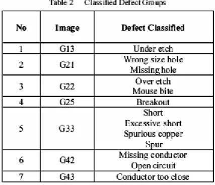
Fig.2.Classified Defect images
The images are named G13, G21, G22, G25, G33, G42 and G43 as is Figure 10. G 13 is generated from the square segment, G21, G22 and G23 from the hole segment, G33 from the thick-line segment and G42 and G43 from the thinline segment. The defects classified by these groups[15][16].
ISSN(Online): 2320-9801
ISSN (Print) : 2320-9798
I
nternational
J
ournal of
I
nnovative
R
esearch in
C
omputer
and
C
ommunication
E
ngineering
(An ISO 3297: 2007 Certified Organization)
Vol. 3, Issue 9, September 2015
4. Hariharan V.S., Nandlal B., Srilatha K.T., "Efficacy of various root canal irrigants on removal of smear layer in the primary root canals after hand instrumentation: A scanning electron microscopy study", Journal of Indian Society of Pedodontics and Preventive Dentistry, ISSN : 0970-4388, 28(4) (2010) pp.271-277.
5. M. Moganti, F. Ercal, C.H. Dagli, and S. Shunekawa, 'Automatic PCB Inspection Agorithm: A Survey', 1996, 63. No. 2.
6. Udayakumar R., Khanaa V., Kaliyamurthie K.P., "Optical ring architecture performance evaluation using ordinary receiver", Indian Journal of Science and Technology, ISSN : 0974-6846, 6(S6) (2013) pp. 4742-4747.
7. T. Taniguchi, D. Kacprzak, S. Yamada, M. Iwahara, and T. Miyogashi, 'Defect Detection on Printed Circuit Board by using Eddy-Current Technique and Image Processing', 101 Press, 2000
8. B.Vamsi Krishna, Starting Inrush Current Control of Three-Phase Induction Motors for Dispersed Generating Systems, International Journal of Advanced Research in Electrical, Electronics and Instrumentation Engineering, ISSN (Online): 2278 – 8875,pp 6411-6422, Vol. 2, Issue 12, December 2013
9. Kanniga E., Selvaramarathnam K., Sundararajan M., "Embedded control using mems sensor with voice command and CCTV camera", Indian Journal of Science and Technology, ISSN : 0974-6846, 6(S6) (2013) pp.4794-4796.
10. Wen-Yen Wu, Mao-Jiun J.Wang and Chih-Ming Liu, 'Automated Inspection of Printed Circuit Board Through Machine Vision', 11. Computers in Industry, 28 (1996) pp.I03-III.
12. Udayakumar R., Khanaa V., Kaliyamurthie K.P., "Performance analysis of resilient ftth architecture with protection mechanism", Indian Journal of Science and Technology, ISSN : 0974-6846, 6(S6) (2013) pp. 4737-4741
13. Z. Ibrahim, S.A.R AI-attas and Z. Aspar, 'Analysis of the Wavelet-Based Image Difference Algorithm for PCB Inspection', in proceedings of SICE, Osaka, Japan, 2002
14. Z. Ibrahim, S.A.R AI-attas, Z. Aspar and M.M. Mokji 'Performance Evaluation of Wavelet-based PCB Defect Detection and Localization Algorithm', in proceedings of ICIT, 2002, Bangkok, Thailand
15. Z.lbrahim, S.A.R AI-attas and Z. Aspar, 'Coarse Resolution Defect Localization Algorith for an Automated Visual PCB Inspection', Jurnal Teknologi, 37(D) Dis. 2002: 79-92
16. A.Geetha, Face Recognition Using OPENCL, International Journal of Advanced Research in Electrical, Electronics and Instrumentation Engineering , ISSN (Print) : 2320 – 3765, pp- 7148-7151, Vol. 3, Issue 2, Febuary 2014.
17. R. Heriansyah. 'Classification of Defect on Bare PCB using Neural Network Technique', Masters Thesis, Universiti Teknologi Malaysia. 2004.
18. D.M. Tsai and B.T. Lin, 'Defect Detection of Gold-Plated Surfaces on PCBs Using Entropy', Int J. Adv Manuf Technol (2002) 20:420-428 19. A.Geetha, Universal Asynchronous Receiver / Transmitter (UART) Design for Hand Held Mobile Devices, International Journal of Advanced
Research in Electrical, Electronics and Instrumentation Engineering, ISSN: 2231-5381, pp 25-26, Volume 3 Issue 1 No1 – January 2012. 20. B.Mehala, Mrs.Anitha Sampath Kumar, Design and Implementation of Resonant Circuit Based On Half-Bridge Boost Rectifier with Output
Voltage Balance Control, International Journal of Advanced Research in Electrical, Electronics and Instrumentation Engineering, ISSN (Online): 2278 – 8875,pp 9370-9378, Vol. 3, Issue 5, May 2014