Abstract
WASHINGTON, JOSEPH ST. PAUL. The Local Structure and Kinetics of Ge-Sb-Te Phase Change Materials for use in Solid State Applications. (Under the direction of Michael A. Paesler and Gerald Lucovsky.)
Recent interest in phase change materials (PCMs) for non-volatile memory
applications has been fueled by the promise of scalability beyond the limit of conventional DRAM and NAND flash memory. Typical PCMs such as Ge2Sb2Te5 (GST) require
significant nitrogen doping to shift their crystallization temperature (Tx) sufficiently above
standard CMOS device operation ranges (~ 80ºC ) but also well below the melting point for thermal stability. Reactive ion etching (RIE) in an Ar/Cl2/CHF3 plasma chemistry is another
crucial step en-route to fabricating energy efficient, high density, nano-scaled PCM memory devices, yet it can lead to unfavorable, irreversible modification of the GST material.
Chalcogens such as Te in GST can easily diffuse and interact unfavorably with the adjacent materials in the device structure thus negatively impacting the lifetime of a PCM device cell. In light of these implications for the final solid state device, it is necessary to understand and articulate the nature and structural implications of doping/alloying GST, the local structural changes that occur post etch processing, and the nature of the Ge-Sb binary and the Ge-Sb-Te ternary alloys.
point to the formation of preferential Ge-N bonding in a chemically ordered germanium nitride local bonding environment in as-deposited and annealed films.
XAFS of various GeSb and Ge-Sb-Te glasses in the binary and ternary systems, in conjunction with time resolved XRD, show that Te in thin films of GeSb with gradually increasing Te atomic concentration prevents phase segregation, promotes stability, and induces nucleation. A multi-edge refinement of as-deposited thin films of Ge2Sb2Tex (x=4, 5,
6, 7), shows that Ge-Sb bonds are present in Ge2Sb2Te4 and Ge2Sb2Te5 from EXAFS fits, and
these Ge-Sb bonds can also be isolated in the Ge near edge spectra in light of inelastic losses, i.e. shake-up / shake-off effects.
The Local Structure and Kinetics of Ge-Sb-Te Phase Change Materials for use in Solid State Applications
by
Joseph St. Paul Washington
A dissertation submitted to the Graduate Faculty of North Carolina State University
in partial fulfillment of the requirements for the Degree of
Doctor of Philosophy
Physics
Raleigh, North Carolina
2010
APPROVED BY:
___________________________ ___________________________ Eric A. Joseph
___________________________
John E. Rowe
___________________________ Nicholas C.M. Fuller
___________________________
David E. Aspnes
___________________________ Gerald Lucovsky
Co-Chair of Advisory Committee
Dedication
I dedicate this work to my parents, Winston and Vivienne, and my older brothers, Sean, Jumbo, and Mark. My deepest desire is that we should experience true love, peace, joy, happiness, and fulfillment, which only comes from intimate relationship with God through belief in the redemption put in effect by His Son, Jesus Christ.
This milestone is testimony to the faithfulness of Our Father. In His love, He has never given me what I deserved, and so I hope to glorify Him with the rest of my life:
∼ Be still, know that I am God. – Psalm 46: 11
∼ Not to us, O Lord, not to us, but to your name be the glory, for the sake of your love and
faithfulness. – Psalm 115: 1
∼ What have you, that you have not received? And if you received it, why are you proud, as
if you did not receive it? – 1 Corinthians 4: 7
∼ By the grace of God, you have been saved through faith. This has not come from you: it is
Biography
Joseph St. Paul Washington was born in St. Andrew, Jamaica on November 21st, 1983, to Winston and Vivienne Washington. After obtaining his high school diploma from St. George’s College (Kingston, Jamaica), he accepted a full scholarship to attend Bethune-Cookman College (Daytona Beach, FL), where he enrolled in August 2001. Over the next 4 years, he grew, matured, and excelled, and finally celebrated graduation with Bachelor of Science (B.Sc.) degrees in Computer Science and Physics in May 2005. His imagination and fascination with computer hardware and solid state devices, and the attractive notion of being paid to go to school, led him enroll in the Physics graduate program at North Carolina State University (Raleigh, NC). Soon after passing the Doctor of Philosophy (Ph.D.) departmental qualifying exam, he was pursuing X-ray absorption spectroscopy studies of phase change materials and chalcogenides under the guidance of Michael Paesler. His early years under Michael’s supervision were characterized by significant learning and appreciation of EXAFS and chalcogenides, made possible by numerous synchrotron based studies, and group
meetings and classes with Gerald Lucovsky, Satish Agarwal, and Dave Baker. His later years built upon these foundations laid at NCSU, which saw Joseph grow exponentially as a
Acknowledgements
I am thankful to the innumerous faculty, friends, and family who have supported, loved, cared for, prayed for, taught, mentored, coached, encouraged, nourished and sheltered me from the very beginning in Daytona Beach, FL, right up to this point, in Raleigh, NC. You have all positively influenced everything about me, from my acquired southern vernacular to my worldview and theology. I am positively indebted to you all!
messages, and emails. We also shared great meals and great memories from my internships and research projects at IBM, including summer corporate league football, and fun times exploring Long Island, NY. My manager during my internship at IBM, Ying Zhang, and a host of other ‘IBMers’ who have befriended me and collaborated with me, notably Simone Raoux and Jean Jordan-Sweet, cannot be thanked enough for their help in making this dissertation possible.
Table of Contents
List of Tables ... x
List of Figures ... xii
Chapter 1 Introduction ... 1
1.1 The Structural Implications of Nitrogen doping in GST ... 3
1.2 The Structural Implications of Reactive Ion Etching N-GST ... 5
1.3 The local structure of GeSb & the role of Te in the Ternary System ... 6
1.4 Outline of the rest of this Dissertation ... 8
Chapter 2 The Structural Implications of Nitrogen doping in GST ... 10
2.1 Amorphous N-GST ATR-FTIR Measurements ... 11
2.2 Amorphous N-GST ATR-FTIR Results and Analysis ... 13
2.3 Amorphous N-GST Depth Profile XPS ... 15
2.4 The EXAFS Equation ... 17
2.5 Amorphous N-GST XAFS Analysis ... 21
2.5.1 Near Edge Analysis ... 23
2.5.2 EXAFS Analysis ... 28
2.5.3 EXAFS Models and Fitting ... 33
2.6 In-situ Time Resolved XRD of N-GST ... 40
2.7 XAFS of 5%N-GST versus Anneal Condition ... 43
2.8.1 EXAFS Data Analysis and Fitting ... 49
2.8.2 The Nature of Crystalline N-GST ... 55
Chapter 3 Phase Segregation in binary GexSb(1-x) ... 59
3.1 GexSb(1-x) EXAFS studies... 60
3.1.1 GexSb(1-x) EXAFS Fits and Modeling ... 65
3.1.2 EXAFS vs XRD in annealed 15:85 ... 71
3.2 EXAFS of as-deposited (Ge15Sb85)xTe(1-x) & (Ge50Sb50)xTe(1-x) ... 75
3.2.1 EXAFS of the amorphous 15:85+Te & 50:50+Te ... 76
3.3 EXAFS vs XRD of annealed (Ge15Sb85)xTe(1-x) & (Ge50Sb50)xTe(1-x) ... 83
3.3.1 EXAFS vs XRD of annealed 15:85+Te ... 83
3.3.2 EXAFS vs XRD of annealed 50:50+Te ... 89
3.4 EXAFS of as-deposited Ge2Sb2Tex ... 93
3.4.1 EXAFS analysis of as-deposited Ge2Sb2Tex (x=4,5,6,7) ... 95
Chapter 4 Conclusions ... 103
References ... 107
Appendices ... 120
Appendix 1 - An Introduction to EXAFS Theory ... 121
Appendix 2 - Experimental Details ... 126
Appendix 4: (JNCS Submitted) Analysis of the forgotten parts of the Ge K edge spectra: life beyond the EXAFS oscillations! ... 138
Appendix 5: Ge and Sb K edge EXAFS Fit Results calculated for the 400°C annealed GexSb(1-x) samples. ... 146
List of Tables
Table 2-1: Calculated penetration depth (dp ), and the estimated final depth after passing
through a 100nm and 1000nm thick sample, for the spectral range observed. ... 12
Table 2-2. Summary of Programs used for XAFS Analysis ... 22
Table 2-3: Final fitting statistical parameters for N-GST samples showing the Fourier
transform ranges (∆k), fitting ranges (∆R), the R factor for each data set (R). The MDS results shown: the number of independent parameters used in the fits (Nind), the number
of variables (Nvar), the chi-squared (χ2), the reduced chi-squared (χ2v), the R factor, and
the measurement uncertainty in R (ε). ... 37
Table 2-4: A summary of the fitting parameters calculated from the fits to the amorphous N-GST samples and their percent errors (the fitting results of undoped N-GST is shown and discussed in chapter 4). In total, 16 parameters are determined from the three data sets. S02 was 0.8 for all data sets... 37
Table 2-5: Background removal quantities used in AUTOBK for Ge K edge N-GST crystallized samples. The EO values is not shown since all samples were aligned to a
common EO of ~11097eV. ... 43
Table 2-6: Final fitting statistical parameters for 250C_RAMP and 250C_10MIN showing the Fourier transform ranges (∆k), fitting ranges (∆R), the R factor for each data set (R). The MDS results shown: the number of independent parameters used in the fits (Nind),
the number of variables (Nvar), the chi-squared (χ2), the reduced chi-squared (χ2v), the R
factor, and the measurement uncertainty in R (ε). ... 50
Table 2-7: A summary of the fitting parameters calculated from the fits to the 250C_RAMP and 250C_10MIN samples and their percent errors. In total, 22 parameters are
determined from the two data sets. S02 was 0.8 for all data sets. ... 52
Table 2-8: Background removal quantities used in AUTOBK for Ge K edge N-GST crystallized samples. The EO values are not shown since all samples were aligned to a
common EO of ~11103eV. The FCC_0.0% sample was capped with a thin layer of Nb to
prevent surface oxidation, so we increased Rbkg to remove to low R background signal. We were unable to collect similar range of data for FCC_6.1% due to beamline power outage. ... 55
Table 3-1: Final fitting statistical parameters for Ge and Sb K edges for amorphous 15:85 and 50:50 showing the Fourier transform ranges (∆k), fitting ranges (∆R), the R factor for each data set (R), the number of independent parameters used in the fits (Nind), the
number of variables (Nvar), the chi-squared (χ2), the reduced chi-squared (χ2v), the R
factor, and the measurement uncertainty in R (ε). ... 66
Table 3-2: A summary of the fitting parameters calculated from the fits to the amorphous GexSb(1-x) samples and their percent errors. Each alloy shows both the parameters from
the Ge edge as well as the Sb edge. In total, 71 parameters are determined from the 10 data sets (5 samples, 2 edges). S02 was 0.8 for all Ge edge data and 0.9 for all Sb edge
Table 3-3: Final fitting statistical parameters for Ge and Sb K edges for a-15:85+Te and 50:50+Te showing the Fourier transform ranges (∆k), fitting ranges (∆R), the R factor for each data set (R), the number of independent parameters used in the fits (Nind), the
number of variables (Nvar), the chi-squared (χ2), the reduced chi-squared (χ2v), the R
factor, and the measurement uncertainty in R (ε). 15:85+Te samples were fit together in a MDS, as were 50:50+Te, and shared parameters are shown in parentheses () and brackets []. ... 79
Table 3-4: A summary of the fitting parameters calculated from the fits to the amorphous 15:85+Te and 50:50+Tesamples and their uncertainties. In 15:85+Te, 16 parameters are determined from the 2 data sets while in 50:50+Te, 20 parameters were calculated from 3 data sets. S02 was 0.8 for all data sets. ... 79
Table 3-5: Background removal quantities used in AUTOBK for Ge, Sb, and Te K edges in Ge2Sb2Tex samples. ... 95
Table 3-6: Final fitting statistical parameters for Ge, Sb and Te K edges for amorphous 225 showing the Fourier transform ranges (∆k), fitting ranges (∆R), the R factor for each data set (R), the number of independent parameters used in the fits (Nind), the number of
variables (Nvar), the chi-squared (χ2), the reduced chi-squared (χ2v), the R factor, and the
measurement uncertainty in R (ε). ... 96
Table 3-7: A summary of the fitting parameters calculated from the fits to the amorphous Ge2Sb2Tex samples and their uncertainties. S02 was 0.85 for all Sb and Te edge data, and
0.7 for Ge edges. ... 98
List of Figures
Figure 2-1: FTIR spectra showing % Absorbance vs wavenumber for N-GST samples and a bare Si wafer. The titles in B, C, and D refer to the film thickness (nm) and N flow rate (sccm.) used for deposition. The fine dashed lines are fits to the spectra, with the fitting range indicated by vertical dashed lines. ... 14
Figure 2-2: Comparison of depth profiled XPS Ge 2p3/2 binding energy spectra for A) 5%N-GST and B) 5%N-GST. The 5%N-5%N-GST spectra represents a depth of ~34nm versus ~17nm for the GST sample. The dashed line in both spectra shows the binding energy of the final depth profile. ... 16
Figure 2-3: A comparison of the un-normalized and normalized Ge K edge absorption data for 5%N-GST. The solid black line was 1000nm thick film on glass substrate, measured at the APS, MRCAT beamline ID-10, using Ar / N mixture in the ionization chamber. The gray dashed line was 100nm film on a bare Si wafer, measured at the NSLS, NIST X23A2 beamline. On either occasion, fill gases of different ratios of Ar / N were used in the ionization chamber. ... 24
Figure 2-4 : Normalized Ge near edge comparison of as deposited 6.1%N-GST (black dotted line), 5%N-GST (black dashed line), 2.5%N-GST (gray solid line), and GST (black solid line). The feature that is scaling with nitrogen concentration is indicated just past the white line. ... 25
Figure 2-5: (A) Near Edge Spectra of beta-Ge3N4 (arrow indicates the main identifying
feature for these) and (B) Fourier transformed EXAFS spectra for beta-Ge3N4
(Republished from[62]). ... 26
Figure 2-6: (A) Near Edge Spectra of a-GeN and (B) Magnitude of Fourier transformed EXAFS spectra of a-GeN. The χ(k) data used for the Fourier transform, used a data range, ∆k = 3 - 13 Ǻ-1, and followed our typical background removal procedures. ... 27
Figure 2-7: Athena screen shot showing background removal parameters (used in AUTOBK) for N-GST samples. The k range is the range over which a spline using Nknots knots was
optimized to approximate the background function. E0 is typically set to the maximum of first derivative of and can be used to align multiple data sets. K-wieght also us to further tune to frequencies to be minimized below Rbkg. Pre-edge and normalization range specifies the range used to define the pre-edge and post-edge lines. Spline range defines the range over with AUTOBK minimizes the background. ... 29
Figure 2-8: x(k) extracted from the µ(E) of as-deposited 6.1%N-GST (black dotted line), 5%N-GST (black dashed line), 2.5%N-GST (gray solid line), and GST (black solid line), using the AUTOBK program. Each spectrum is the average of at least four florescence measurements. Each x(k) function is multiplied by k2 to emphasize the high-energy oscillations, as shown on the y-axis. ... 29
solid line), using a window range of ∆k = 3-13.5 Ǻ-1. The gray line shows the
background feature. ... 30
Figure 2-10: (A-D): Fits to the Ge K edge as-deposited N-GST data for A) GST, B) 2.5%N-GST, C) 5%N-2.5%N-GST, and D) 6.1%N-GST. Magnitude of the complex Fourier
transformed of EXAFS spectra is shown. The solid black line is the data, and gray dash line is the fits. ... 38
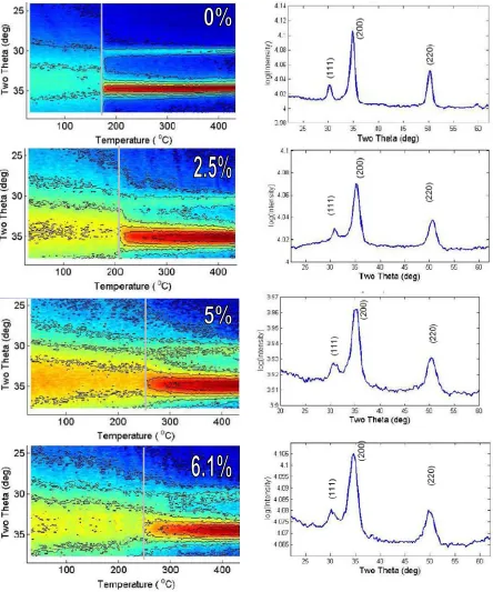
Figure 2-11: Intensity of diffracted x-ray peaks is plotted vs diffraction angle (2θ) over a range of 15° (vertical axis) vs temperature (horizontal axis) for blanket films of GST and 5%N-GST heated at a rate of 1 °C/s. This is shown alongside the Intensity vs (2θ) which was taken at 450°C. Transitions to the crystalline rocksalt phase are marked by vertical solid gray lines, corresponding to 175°C, 215°C, 250°C, and 250°C for 0%, 2.5%, 5%, and 6.1%N-GST, respectively. The cubic peak indices are shown. ... 42
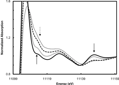
Figure 2-12: Normalized Ge near edge comparison of AS_DEP (black dotted line), 250C_RAMP (black dashed line), 250C_10MIN (gray solid line), and 300C_30MIN (black solid line). Arrows indicate the appearance of sharp features relating the long range order in GST ... 44
Figure 2-13: x(k) extracted from the µ(E) of AS_DEP (black dotted line), 250C_RAMP (black dashed line), 250C_10MIN (gray solid line), and 300C_30MIN (black solid line), using the AUTOBK program. Each spectrum is the average of at least four florescence measurements. ... 44
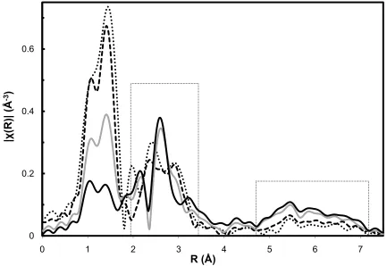
Figure 2-14: Magnitude of Fourier transformed EXAFS spectra AS_DEP (black dotted line), 250C_RAMP (black dashed line), 250C_10MIN (gray solid line), and 300C_30MIN (black solid line), using ∆k = 3-15Å ... 45
Figure 2-15: The steady state nucleation rate [97] of GST as a function of time, reaches a maximum at about 250°C. The dashed line corresponds to the amorphous to FCC crystalline transition temperature for GST sample as observed in in-situ XRD in figure 2-11. (Republished from [98] © JAP 2004) ... 48
Figure 2-16: Fits to the Ge K edge for (A) 250C_RAMP and (B) 250C_10MIN. Magnitude of the complex Fourier transformed of EXAFS spectra is shown. Solid black line = data, gray dashed line = fit. ... 51
Figure 2-17: Normalized Ge near edge comparison of FCC_0.0% (solid black line),
FCC_2.5% (gray dashed line), FCC_5.0% (black dashed line), FCC_6.1% (black dotted line). The solid black arrow indicates sharp features relating the long range order in GST, while dashed arrow at the near edge indicates the region increasing with N at %.56
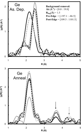
Figure 2-18: Magnitude of the complex Fourier transformed EXAFS spectra of FCC_0.0% (solid black line), FCC_2.5% (gray dashed line), FCC_5.0% (black dashed line), FCC_6.1% (black dotted line) their respective using ∆k values shown in table 2-5. The Ge-N 1st shell is clearly distinguishable between 1 - 2Å. The box between 2 – 3.5 Å is crystalline GST first shell, where there is variation between the samples. The box
Figure 3-1: Comparison of the magnitude of the complex FT of the Ge K edge EXAFS for as deposited (top) and the 400°C annealed (bottom) 75:25 (solid black line), 50:50 (dash gray line), 25:75 (solid gray line), 15:85 (black dashed line), 7:93 (black dotted line), and Ge metal foil (gray dotted line). Background removal quantities used in AUTOBK for both amorphous and annealed GexSb(1-x) samples are shown in the inset. The EO
values are not shown since all samples were aligned to a common EO of ~11102eV for
Ge analysis. ... 61
Figure 3-2: Comparison of the magnitude of the complex FT of the Sb K edge EXAFS for as deposited (top) and the 400°C annealed (bottom) 50:50 (dash gray line), 25:75 (solid gray line), 15:85 (black dashed line), 7:93 (black dotted line), and Sb metal foil (gray dotted line). Background removal quantities used in AUTOBK for both amorphous and annealed GexSb(1-x) Sb edges are shown in the inset. The EO values are not shown since
all samples were aligned to a common EO of ~30491eV for Sb analysis. ... 62
Figure 3-3: Basic structural models for tetrahedrally bonded Ge and trigonal pyramidal coordinated Sb. ... 65
Figure 3-4: Fits to the Ge and Sb K edge for 15:85 (top) and 50:50 (bottom). Magnitude of the complex Fourier transformed of EXAFS spectra is shown. Solid black line = data, gray dashed line = fit. These fits are representative of the typically good fit to data obtained in all amorphous and annealed GexSb(1-x) . ... 68
Figure 3-5: Ge-Sb bonding fraction calculated from the Ge edge (black line), versus the Sb-Ge bond fraction calculated at the Sb edge (gray line) of the Sb-GexSb(1-x). We can compare
the fraction of Ge atoms bonded to Sb (as opposed to Ge-Ge bonds) and the fraction of Sb environment bonded to Ge (as opposed to Sb-Sb). ... 70
Figure 3-6: In situ XRD of 15:85 film during a 1°C/min ramp anneal in He. At
crystallization, Bragg peaks of Sb with Ge in solid solution are seen. Ge (111) peak appears at 375°C (from ref [114]). ... 71
Figure 3-7: Comparison of the magnitude of the complex Fourier transform of the EXAFS data at the Ge K edge15:85 as deposited (black dash line), after a 300°C ramp/quench (gray solid line), and after a 400°C 30 minute anneal (solid black line). ... 72
Figure 3-8: Fits to the Ge K edge for 15:85 after a 300°C ramp/quench. Magnitude of the complex Fourier transformed of EXAFS spectra is shown. Solid black line = data, gray dashed line = fit. For convenience, we show the calculated fit variables and the
statistical goodness- of- fit parameters in the figure. ... 74
Figure 3-9: Comparison of the magnitude of the complex Fourier transform of the Ge K edge EXAFS for the as deposited (A) 15:85+Te and (B) 50:50+Te, for samples with no Te (solid black line), 10% Te (solid gray line), 20% Te (black dashed line), and 33% Te (gray dashed line). ... 77
Figure 3-10: Fits to the Ge K edge for 15:85 +10 (20) and 50:50+10 (20, 33) samples.
Figure 3-11: Change in bonding fraction of Ge-Ge (black dashed line), Ge-Sb (gray dashed line), and Ge-Te (gray solid line) at the Ge K edge in 15:85 and 50:50 with increasing Te content. ... 82
Figure 3-12: Intensity of diffracted x-ray peaks is plotted vs diffraction angle (2θ) over a range of 15° (vertical axis) vs temperature (horizontal axis) for blanket films of
15:85+10 and 15:85+20 heated at a rate of 1°C/s. This is shown alongside the Intensity vs (2θ) which was taken at 450°C. Transitions due to the crystalline Sb rhombohedral phase are marked by vertical solid gray lines. The black dotted arrows show un-indexed features. The Sb rhombohedral peak indices are indicated. ... 84
Figure 3-13: Normalized Ge near edge comparison of 300°C annealed 15:85 (solid black line), 15:58+10 (solid gray line), and 15:85+20 (black dashed line). The intensity of the white line, and the appearance of sharper near edge features coincide with Te addition. ... 86
Figure 3-14: Comparison of the magnitude of the complex Fourier transform of the Ge K edge EXAFS for 300°C annealed 15:85 (solid black line), 15:58+10 (solid gray line), and 15:85+20 (black dashed line). The arrows show the appearance of long range order in 15:85+20. ... 86
Figure 3-15: Intensity of diffracted x-ray peaks is plotted vs diffraction angle (2θ) over a range of 15° (vertical axis) vs temperature (horizontal axis) for blanket films of 50:50+10, 50:50+20, and 50:50+33, heated at a rate of 1°C/s. This is shown alongside the intensity vs (2θ) which was taken at room tempaerture after a ramp to 450°C. The Sb and Ge crystal peak indices are indicated, as well as the NaCl cubic phase indices in 50:50+33. ... 88
Figure 3-16: Comparison of (A) the normalized Ge near edge and (B) the magnitude of the complex Fourier transform of 450°C annealed 50:50 (solid black line), 50:50+10 (solid gray line), 50:50+20 (black dashed line), and Ge foil (black dotted line). ... 90
Figure 3-17: Normalized Ge near edge comparison of 450°C annealed 50:50+33 (solid black line) to 300°C annealed GST (solid gray line). Apart from a change in the intensity of the white line, both share similar near edge features ... 91
Figure 3-18: Comparison of the magnitude of the complex Fourier transform of the Ge K edge EXAFS for 450°C annealed 50:50+33 (solid black line) to 300°C annealed GST (solid gray line). ... 92
Figure 3-19: Comparison of the magnitude of the complex Fourier transform of the Ge, Sb, and Te K edge EXAFS for the as deposited 224 (solid black line), 225 (gray dashed line), 226 (solid gray line), and 224 (black dashed line). Only the range of interest (~2 - 3Ǻ) is shown for clarity. ... 97
Figure 3-20: Fits to the Ge, Sb, and Te K edge for amorphous 225. Fit quality is representative of those obtained for 224, 226, and 227. Magnitude of the complex Fourier transformed of EXAFS spectra is shown. Solid black line = data, gray dashed line = fit. ... 100
Chapter 1
Introduction
S. R. Ovshinsky was first to propose and patent [1] the notion of a memory switch based on distinct material properties of the amorphous and crystalline phases of multi-component chalcogenides in the 1960’s [2]. In the late 1980s, Matsushita / Panasonic developed chalcogenide based phase-change optical disc technology that remained stable over a million cycles [3], leading to widespread adoption of optical disk memory and
resulting in the commercialization of the 4.7 GB digital versatile disc random access memory (DVD-RAM) in the 1990s. More recent interest focuses on the creation of a new solid state phase change memory (PCM) which would bypass the scalability concerns of the current technology (NAND, NOR, DRAM, FLASH) [4] while simultaneously improving latency and power consumption, as well as ensuring non-volatility and radiation hardness [5]. Of course, there are obstacles. Typical PCM materials such as Ge2Sb2Te5 (GST) require significant
doping (or alloying) to shift their crystallization temperature (Tx), sufficiently above standard
CMOS device operation ranges (~ 80ºC ) but also well below the melting point for thermal stability [6]. Etch processing is a crucial step en-route to fabricating energy efficient, high density, nano-scaled PCM memory devices, yet it can lead to unfavorable, irreversible modification of the GST material [7]. Chalcogens such as Te in GST can easily diffuse and interact unfavorably with the adjacent materials in the device structure thus negatively impacting the lifetime of a PCM device cell [8].
problems manifest themselves in the widespread difficulty of probing the local atomic environment of the PCM at the point of phase change. A direct consequence of this is the unclear structural role of the chalcogen in facilitating crystal nucleation and growth. This leads to ambiguity in the role of local structure in determining material properties. Many local structural studies have focused on mainstream PCMs utilized in optical disc technology, such as GST and AgInSbTe (AIST). These studies confirm X-ray Absorption Spectroscopy (XAS) as an ideal tool for probing the atomic environment of these PCMs, since sample crystallinity is not a precondition. XAS includes both the X-ray absorption near edge structure (XANES) and the extended X-ray absorption fine structure (EXAFS) spectroscopies, where XANES is useful for determination of the valence state and coordination geometry, while EXAFS can reveal the local molecular structure about the absorbing element in the sample. XAS is typically more conclusive when used in conjunction with X-Ray Diffraction (XRD), X-ray Photoelectron Spectroscopy (XPS), Fourier Transform Infrared Spectroscopy (FTIR), Transmission Electron Microscopy (TEM), or other
techniques to illuminate the relationship between the structural configuration of the amorphous and crystalline phases and the observed thermal, optical, electrical, and mechanical properties of the system.
Carolina State University in Raleigh, NC and the IBM/Macronix PCRAM Joint Project at the IBM T.J. Watson Research Center, in Yorktown Heights, NY. The experiments are all in timely response to urgent, pertinent questions on the correlation of the PCM’s local structure to observed physical characteristics at various stages of material preparation for solid state memory device fabrication. While these experiments allow one to add to the already widespread discussion of the nature of the amorphous and crystalline phases of GST, they also address the nature and structural implications of doping/alloying GST, the local
structural changes that occur post etch processing, and the nature of the Ge-Sb binary and the Ge-Sb-Te ternary alloys. The combination of XANES and EXAFS are complemented
through the use of XRD, FTIR, and XPS in the belief that a complex structural system is often best understood in light of numerous experimental probes, with each providing correlative and unique data.
1.1 The Structural Implications of Nitrogen doping in GST
In semiconductor nomenclature, doping refers to the introduction of donor (e.g. arsenic) or acceptor (e.g. boron) impurities into an intrinsic semiconductor in order to change the equilibrium carrier concentration. This results in either extrinsic n-type (donors) or p-type (acceptors) containing new dopant related energy levels in the band gap close to the
conduction band or valence band, respectively [9]. In this formalism, GST can be
structure (Fermi level located close to valence band) [11; 12], and a degenerate p-type semiconductor (metallic character, i.e Fermi level in valence band)in the hcp structure [12]. The term “doping” as it relates to GST, however, is a misnomer. Experimentally, GST has been tested with various dopants including nitrogen [13; 14; 15], tin [16], silicon [17], and oxygen [18], where typical dopant atomic concentrations are between 2% and 10%, which is 3-4 orders of magnitude higher than typically 0.001% atomic concentration of Ar in intrinsic Ge. Unlike an electrical response to impurity doping in Si and Ge semiconductors, doping in GST is meant to modify the material properties of the PCM. In previous studies of the optical and structural properties of nitrogen-doped GST (N-GST), the addition of nitrogen lead to grain refinement [19], crystal lattice distortions that induced strain in the films, increased resistivity of the amorphous state, and increased temperature for the transition from
amorphous to the metastable, distorted rocksalt phase (Tx) [20]. Tailoring Tx is critical since
GST must be thermally stable over the typical range of temperatures for its solid state operating environment. Previous studies show that thermal cycling (annealing and cooling) of undoped GST films with temperatures from 30 to 80 °C (far less than ~140°C for Tx
of the GST crystallites, forming a locally, chemically ordered Ge-N bonding environment such that the annealed film is comprised of crystallites with a dopant rich grain boundary.
1.2 The Structural Implications of Reactive Ion Etching N-GST
Scalability limitations far below the threshold of current memory technology represents one of phase change memory’s most appealing attributes. Current metal oxide semiconductor field effect transistors (MOSFETs) and floating gate transistors, which are the fundamental building blocks of current NAND and NOR flash memory and DRAM, begin to suffer from reduced device performance when scaling beyond the 22nm node. As an
example, quantum mechanical modeling has projected a gate oxide scaling limit of 20 Å before which chip standby power will become excessive due to electron tunneling currents [23]. The scalability of PCM based memory, on the other hand, suffers no physical
limitations into the next 3-4 lithography generations [24] as 3nm doped eutectic Ge-Sb PCM bridge prototype memory cells have been recently reported [25]. Although fundamentally this may indicate that PCM based memory technology is easily scalable, one area in which scalability is still under evaluation is within the arena of materials processing and device fabrication. Reactive ion etching (RIE) in an Ar/Cl2/CHF3 plasma chemistry allows
More importantly, this study concludes that this layer penetrates to a thickness approximately 10nm into the material and shows the process to be chemically driven (independent of ion bombardment). A subsequent submission to the Journal of Applied Physics, shown in appendix 3, examines the chemical and structural effects of this etch modification layer and its implications for device performance and crystallization, from XPS, X-ray absorption fine spectroscopy (XAFS), time resolved laser reflectivity and time resolved X-ray diffraction (XRD). Laser reflectivity data shows that etch modification hinders nucleation in the optical device by changing the interfacial properties of the surrounding dielectric medium. In situ XRD data shows that the transition from the FCC to HCP phase is increased as a result of the etch modification layer, and this is likely due to formation of an oxide which desorbs at the HCP crystallization temperature. This oxide was confirmed by depth profiled XPS, as well as XAFS of partially and fully etch films. XAFS results revealed the nature of the etch
modification region resulting from fluorine and chlorine etch chemistries, to consist of significant amorphous GeO2 and Sb2O3.
1.3 The local structure of GeSb & the role of Te in the Ternary System
refine our data analysis by understanding typically un-used features at the near edge data and correlating these to structural phenomenon.
1.4 Outline of the rest of this Dissertation
This dissertation is a discourse on the structure-property relationships of PCMs obtained by combining EXAFS and XANES with complementary spectroscopies. Each chapter presents experiments, results, and discussions meant to illuminate the local structure of Ge-Sb-Te containing PCM, as it is modified for solid state memory applications. In chapter 2, XAFS, FTIR, XRD, and depth profiled XPS results on as-deposited and annealed N-GST films are presented along with a detailed description of the experiment and analysis. We discuss the implications of a predominantly germanium nitride dopant environment and relate this to the shift in Tx, as well as the observed grain refinement in TEM. Furthermore, a
discussion of observed long range order of the N-GST crystalline environment raises important questions for future studies, but also emphasizes the distinct, separate dopant environment pre / post anneal. In chapter 3, we present a combined XAFS study of GexSb(1-x)
(x=75, 50, 25, 15, 4) glasses together with the implications as Te is gradually added to the binary system. XAFS results of interesting ternary samples, including (Ge15Sb85)xTe(1-x) ( x =
0.9, 0.8), (Ge50Sb50)xTe(1-x) (x = 0.9, 0.8, 0.66) and Ge2Sb2Tex (x=4,5,6,7) are presented in
Chapter 2
The Structural Implications of Nitrogen doping in GST
The primary purpose of nitrogen doping is to advantageously modify the material properties of the GST system. These effects can be understood structurally via a combination of XAFS (XANES and EXAFS), FTIR, XPS, and XRD, where the in-situ time resolved XRD measurements and depth-profiled XPS measurements were performed by others. Chapter 2 is organized as follows. In section 2.1, we introduce and describe the ATR-FTIR measurements of as-deposited N-GST, while section 2.2 presents the results and analysis of the observed IR vibrational modes. Section 2.3 presents the depth profile XPS of the Ge 2p3/2
spectra of 5 atomic percent nitrogen doped GST (5%N-GST) versus undoped GST. The EXAFS equation is introduced in section 2.4. In section 2.5, we present the as-deposited N-GST XAFS analysis, consistent with our FTIR and XPS data. This section includes the near edge analysis (2.5.1), the local structural analysis from EXAFS (2.5.2) and a description of the modeling and fitting done (2.5.3).
The remaining sections of chapter 2 present the local structural role of the dopant in the crystallization. This is done by comparing in-situ, time resolved, XRD measurements (section 2.6) and XAFS results (section 2.7) for 5%N-GST after various annealing
2.1 Amorphous N-GST ATR-FTIR Measurements
A Nicolet Nexus 870 Fourier transform infrared spectrometer (FTIR) with a Harrick attenuated total reflection (ATR) accessory was used to measure the nitrogen vibrational modes within the N-GST films. The ATR microscope objective contains a small internal reflection element (IRE) fabricated from a pure Ge crystal, and placed at the focus of a Cassegrain optic, i.e the sample contact surface. The contact surface is circular and typically smaller than sample pieces cleaved for measurements. The spectral region examined was from 400 – 4000 cm-1 at a resolution of 4 cm-1 and was detected by a liquid nitrogen cooled MCT detector. N-GST samples were prepared by DC reactive sputtering from a Ge2Sb2Te5
compound target in a mixture of argon and nitrogen feedgas chemistries to thicknesses of 100 nm or 1000 nm on bare Si wafers. The nitrogen flow rate was varied between 0, 13, and 100 sccm for the 100 nm films, but only 100 sccm for the 1000 nm thin film (sccm = standard cubic centimeter per minute at STP). Previous compositional measurements showed that the 13 sccm N flow rate resulted in approximately 5% bulk N atomic concentration.
evanescent wave will be attenuated, and this intensity change will be recorded as the IR light exits the crystal and passes through the spectrometer to the detector. The crystal material used for the IRE affects the measurement; each crystal’s particular refractive index affects the depth of penetration and the occurrence of anomalous dispersion.
Effective depth of penetration into the sample depends on the wavelength of the radiation, the refractive indices of both sample and IRE, and on the angle of incidence of the radiation, as given, to a good approximation, in the equation below first proposed by Harrick [33],
λ
/ [Eqn. 2.1]
where
λ
is the wavelength of the radiation, is the angle of incidence, is the refractive index of the IRE, is the refractive index of the sample and is/ .
Numerous IREs are in use including Ge, Si, ZnSe and diamond (n= 4, 3.4, 2.4 and 2.4, respectively), but we only had access to a Ge objective.Table 2-1: Calculated penetration depth (dp ), and the estimated final depth after passing through a 100nm and 1000nm thick sample, for the spectral range observed.
wave #
(cm‐1) λ (m) (m) 100nm‐ (m) 1000nm‐ (m)
400 2.50E‐05 1.67E‐06 ‐1.57E‐06 ‐6.67E‐07
550 1.82E‐05 1.21E‐06 ‐1.11E‐06 ‐2.12E‐07
700 1.43E‐05 9.52E‐07 ‐8.52E‐07 4.76E‐08
850 1.18E‐05 7.84E‐07 ‐6.84E‐07 2.16E‐07
1000 1.00E‐05 6.67E‐07 ‐5.67E‐07 3.33E‐07
1150 8.70E‐06 5.80E‐07 ‐4.80E‐07 4.20E‐07
1300 7.69E‐06 5.13E‐07 ‐4.13E‐07 4.87E‐07
Using a Ge crystal IRE, a typical angle of incidence of 45˚ and a typical sample refractive index of 1.5, table 2-1 shows the penetration depths , and the resultant
penetration into a 100nm and 1000nm thick sample over the IR spectral range used for our analysis. Table 2-1 shows that over the range of ~ 700 cm-1 and higher wavenumbers, we are more likely to sample within the bulk of a 1000nm thick sample (positive values), and the substrate of the 100nm thick sample (negative values).
2.2 Amorphous N-GST ATR-FTIR Results and Analysis
We measured a bare Si wafer sans N-GST, and noticed that there was significant IR activity, due to impurities in the Si wafer. No analysis was performed on these background spectra, except to approximate the location of these features for subsequent discrimination from the N-GST data. This spectrum was identical to a measurement of 100nm thick, undoped GST, as expected from the expected depth of penetration (100nm-dp), into an IR inactive sample. Figure 2-1 (A) to (D) shows the subsequent measurements of the doped N-GST samples compared to the bare Si wafer. In figure 2-1, there is clearly a doublet feature just between 700-800 cm-1 which scales with N atomic % and film thickness. These absorption features were deconvolved using multiple Gaussian peak fitting in Origin 5.0, where the consistent variation in each spectra was due to peaks at 770 and 720 cm-1. The group formed by a
planar bonded N atom and its three Ge neighbors is the skeletal Ge3N group, with normal
asymmetric stretching vibration involved the displacement of the N as well at the three Ge neighbors; it is the most strongly IR active and has an intensity proportional to the N concentration [35].
Figure 2-1: FTIR spectra showing % Absorbance vs wavenumber for N-GST samples and a bare Si wafer. The titles in B, C, and D refer to the film thickness (nm) and N flow rate (sccm.) used for deposition. The fine dashed lines are fits to the spectra, with the fitting range indicated by vertical dashed lines.
The main absorption features in figure 2-1 at 770 and 720 cm-1 is the asymmetric stretching mode, as previously observed in IR spectroscopic studies of amorphous GexN(1-x)
[36]. More stable compounds of α-Ge3N4 and β-Ge3N4 actually displayed more resemblance
to our spectra [37; 38], the most notable being a plasma nitrided Ge sample hypothesized to (B) 100nm, 13 sccm.
(C) 100nm, 100 sccm. (D) 1000nm, 100sccm.
consist of 80% β-Ge3N4 + 20% α-Ge3N4 having identically observed bands at 780 cm-1 and
730 cm-1 [38]. These results imply an ordered germanium nitride forms in as deposited N-GST, but do not provide an acceptable explanation for this, considering that N-GST films deposited by plasma reactions are expected to be completely amorphous. It is known that the presence of back impurity atoms of a different electronegativity, and even the absence of back atoms, i.e. the inclusion of dangling bonds, influences the charge distribution around the Ge-N dipole, thus changing the position of the absorption band [39; 40]. The resulting shift of the absorption peak may be to lower [41] or higher [42] energies, depending on
electronegativity of the back atom. It is therefore possible that the doublet feature in the N-GST samples in figure 2-1 represents the influence of the Ge-Te and Ge-Sb next nearest neighbor environment on the charge distribution of the Ge-N dipole.
2.3 Amorphous N-GST Depth Profile XPS
XPS spectra were collected about the Ge 2p3/2 binding energy of as-deposited, 100nm
thin films of 5%N-GST and undoped GST, deposited in the manner described in section 2.1. XPS measurements were performed by Dolores Miller, using a Physical Electronics
Quantum 2000 ESCA Microprobe using a monochromatic Al Ka source with a 200 µm spot
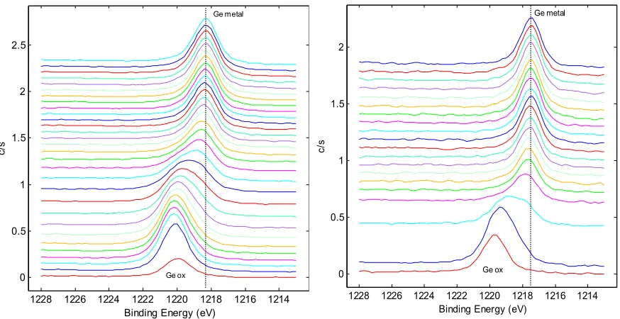
and the analyzer axis. Figure 2-2 shows the results of the first depth profile XPS spectra for 5%N-GST and GST into a depth of approximately 34nm and 17nm, respectively.
The vertical dashed lines in the figure above represent the binding energy of the final depth profile (presumed to be from the metallic Ge bonds as compared to the GeOx bonds at
the near surface) and show that there is a shift in binding energy in 5%N-GST (1218.25) as compared to GST (1217.5). This agrees well with previously published Ge 2p3/2 XPS results
for Ge3N4 (1218.8) [43] and crystalline Ge (1217.38) [44], and provides additional evidence
of a shift in binding energy due to the formation of Ge-N bonding. Furthermore, no similar shifts were observed at Sb or Te 3d peaks. The N 1s peak was present in 5%N-GST, as expected, occurring at a binding energy of ~397.5, which was similar to the 397.4 reported for Ge3N4 [43] but was 0.4eV more than previously observed in N-GST films by others [45] .
1214 1216 1218 1220 1222 1224 1226 1228 0 0.5 1 1.5 2 2.5
Binding Energy (eV)
c/
s
Ge ox
Ge metal
1214 1216 1218 1220 1222 1224 1226 1228 0 0.5 1 1.5 2
Binding Energy (eV)
c/
s
Ge ox
Ge metal
These XPS and FTIR measurements both confirm the formation of Ge-N bonding as nitrogen is added to GST.
2.4 The EXAFS Equation
During XAFS measurements, we record X-ray intensities; that is, the intensity of an incident and transmitted X-ray beam through a given sample, or the intensity of incident and fluorescent X-rays (i.e. fluorescence mode). We obtain the X-ray absorption coefficient
, given by ln ⁄ (transmission) or ⁄ (fluorescence), where , , , and are the sample thickness, and intensities of the incident, transmitted, and fluoresced X-rays, respectively. is the probability for an X-ray to be absorbed by a sample. For an isolated atom, for instance a monoatomic gas, the measured looks roughly like a decaying step function. This step function is broadened by lifetimes of the core hole [46] and of the excited photoelectron, as well as the energy resolution of the
experimental apparatus. For an atom in condensed matter, this broadened, decaying step function is modulated by an oscillatory fine structure associated with the presence of
surrounding atoms. It is this oscillatory structure which is called the EXAFS. We isolate and analyze this in order to yield information of the local structural environment of the excited atom.
surrounding the excited atom [47]. This changed EXAFS from a qualitative effect to a
quantitative one, allowing accurate comparison of experimental data to theoretical models for amorphous solids and complex materials. The derivation and development of modern
EXAFS theory, including important approximations (e.g. self energy effects) and methods of data analysis is covered in detail by others [48; 49; 50; 51]. A conceptually transparent, plane wave approach to the EXAFS equation is shown in appendix 1, which shows off much of the essential physics. This EXAFS equation, is shown in eqn. 2.2 in terms of a sum of the contributions from all scattering paths of the photoelectron:
∑ /
[Eqn. 2.2]
with Δ [Eqn. 2.3]
and
[Eqn. 2.4]
Here is the photo-electron wave vector, or ( ) is the Fermi energy, and is the interatomic distance between the absorber and the coordinating atoms, Δ is the slight (<0.1 Å) calculated change to the interatomic distance relative to the initial , and Δ is the calculated change in the photoelectron energy value used to align the energy scale of the theoretical spectrum to match the measured spectrum.
are amplitude terms, which modify the amplitude of the EXAFS signal and do not have a k-dependence. represents the number of coordinating atoms within a particular shell for single scattering, or it is the number of identical paths (path degeneracy) in multiple
remaining electrons in the presence of the core hole vacated by the photoelectron, and usually has a value between 0.7 and 1.0 [52]. The amplitude is reduced by the term, i.e. contributions diminish for shells of atoms located at increasing distance from the absorber. The amplitude is further modified by , where is the mean-square displacement of the bond length between the absorber atom and the coordinating atoms in a shell. It has contributions from dynamic (thermal) disorder as well as static disorder (structural heterogeneity). Increasing the distribution of distances within a single shell decreases the amplitude of the EXAFS signal because the phase differences between outgoing and scattered photoelectrons are shifted slightly for each atom in the coordination shell. The EXAFS process occurs on the femto-second (10-15 s) time scale, while thermal vibrations occur on a much longer time scale of 10−10 to 10−12 s. Because the atoms are essentially “frozen” at one position about their thermodynamic minima during the excitation process, EXAFS measures the distribution of the distances between the absorber atom and each of the coordinating atoms within a shell in terms of a value.
/ also modifies the amplitude, and is due to inelastic losses in the scattering process. It depends on photoelectron mean free path , and explains why the EXAFS signal is dominated by the scattering contributions from atoms within approximately 10 Å of the absorber atom; this makes EXAFS a local structural probe.
amplitude written in terms of the single scattering formalism [53]. Atoms with more electrons scatter photoelectrons more strongly at higher wavenumbers, and thus
depends on the atomic Z number. This presents a difficulty in distinguishing between the EXAFS signal from say, Ge-N and Ge-O backscatters on the basis of their scattering amplitudes alone.
accounts for the oscillations in the EXAFS equation and describes the path, 2 of the photoelectron, multiplied by to give it its phase. is the phase shift caused by the photoelectron’s interaction with the surrounding atomic environment. It is the Fourier transform of this sine term, which allows us to observe and parameterize separate shells (peaks) at distances related to . However, the peak is not precisely at due to , which causes a shift of ~ -0.5 Å.
Computer programs, such as FEFF, calculates the effective scattering amplitude
2.5 Amorphous N-GST XAFS Analysis
XAS measurements were performed at MRCAT beamline ID-10 [55], at the
Advanced Photon Source (APS) at Argonne National Laboratory, in Argonne, IL as well as NIST beamline X23A2 [56] at the National Synchrotron Light Source (NSLS), Brookhaven National Laboratory, in Upton, NY. Appendix 2 highlights some important experimental considerations, pertaining to the energy selection method (monochromator type,
monochromator slits), harmonic X-ray elimination (detune percentage, type of mirror), focusing optics (KB mirrors, zone plates), the sample geometry (grazing incidence, rotating stage), detector specifications (ionization chambers, solid-state detectors, filters, fill gases), and the incident X-ray beam profile. Effective harmonic rejection is of particular significance for samples containing Ge + (Sb and/or Te) since a typical Si crystal monochromator at the Ge K edge (11103 eV) will diffract, according to Braggs Law, both the fundamental
harmonic (k=1) as well as the third harmonic (k=3). The 3rd harmonic, with energies ~33309 in this case, increases the probability that Sb or Te photoelectrons will be excited, to the detriment of Ge absorption spectrum. The principal XAFS samples were thin films of varyingly doped N-GST deposited to approximately one micron film thickness, at room temperature on 200mm bare Si wafers and 0.2mm glass substrates (for transmission
EXAFS) by DC reactive sputtering a Ge2Sb2Te5 compound target in a mixture of argon and
confirmed by Rutherford Backscattering Spectrometry (RBS), Particle Induced X-ray Emission (PIXE), and Auger Emission Spectroscopy (AES).
Four or more EXAFS spectra were collected for each sample, and these raw data were subsequently aligned and averaged (merged). The merged spectrum, is then normalized using a standard algorithm [48] of pre-edge subtraction and edge-step normalization.
Additionally, the fine structure oscillations are isolated using the AUTOBK [57] program. All important preprocessing features, such as alignment, merging, normalization and
background removal are implemented in a user-friendly manner by ATHENA [58], which is a GUI to IFEFFIT [59]. To model EXAFS spectra, we utilize Athena for background
refinement, and ARTEMIS (another GUI to IFFEFIT) for building structural models and optimizing these versus the experimental data [58]. IFEFFIT is an interactive engine
containing the algorithms for fitting the theoretical FEFF calculations [60]. FEFF calculates well spaced atomic potentials based on the scattering processes from a cluster of atoms, with respect to the absorber atom, providing that an initial structural model (e.g an isomorphic crystal structure) is supplied. Table 2-2 briefly summarizes the computer programs mentioned here.
Table 2-2. Summary of Programs used for XAFS Analysis
Program Purpose Input Output
Athena GUI to IFEFFIT for background removal, normalization,
XANES Analysis, etc.
Absorption data
μ(E)
Norm μ(E), EXAFS χ(k)
and χ(R) spectra
Artemis GUI to IFEFFIT and FEFF for fitting theoretical model to
experimental data
EXAFS χ(k)
spectra
Best fit model / Results
FEFF Calculates Fjeff(k) and Фjeff(k) based on atom cluster. Cluster of Atoms Theoretical EXAFS
IFEFFIT Interactive engine for performing least squares fitting
of FEFF theory to experimental data
2.5.1 Near Edge Analysis
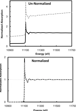
Normalization is particularly important, specifically for a standards based approach to XANES analysis. It negates differences between spectra due to absorber element concentration, measurement type (fluorescence / transmission), sample preparation and thickness, and detector response. Consequently, variations in the near edge are ascribed to differences in local molecular bonding environment and/or allowed electronic states. Figure 2-3 shows a comparison of as deposited, 5% N-GST, Ge K edge absorption spectra taken at different beamlines, with different florescence detectors, before and after normalization.
The normalization process involves a regression to the absorption edge in the pre-edge region (−200 to −30 eV before the edge energy) and the post-edge region (50–1000 eV above the edge energy). We typically regress a linear function to the pre-edge region, and a linear or quadratic function to the post-edge region. These lines are extrapolated to the absorption edge, E0, and the difference in absorption between these projected lines at E0 is
Figure 2-3: A comparison of the un-normalized and normalized Ge K edge absorption data for 5%N-GST. The solid black line was 1000nm thick film on glass substrate, measured at the APS, MRCAT beamline ID-10, using Ar / N mixture in the ionization chamber. The gray dashed line was 100nm film on a bare Si wafer, measured at the NSLS, NIST X23A2 beamline. On either occasion, fill gases of different ratios of Ar / N were used in the ionization chamber.
As shown above, normalization removes detector effects, and allows us to directly compare samples measured under different circumstances. A direct comparison of
normalized as-deposited N-GST near edge spectra vs nitrogen flow rate, shown in figure 2-4,
0 1 2 3 4
10900 11100 11300 11500 11700
Normalized Absorption
Energy (eV)
Un
‐
Normalized
0 1 2
10900 11100 11300 11500 11700
Normalized Absorption
Energy (eV)
reveals a feature just after the absorption edge which clearly scales as a function of nitrogen atomic concentration.
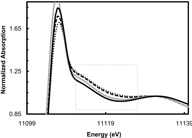
Presuming this is Ge-N related, from our FTIR and XPS study, an understanding of the structural standards for thermally stable Ge-N compounds is required. Of numerous published works characterizing germanium nitride, we obtained the near edge spectra for β -Ge3N4, which exhibits an almost matching feature about 22eV past the edge [61], shown in
figure 2-5 (A) with an associated EXAFS spectrum shown in figure 2-5(B) [62].
0.85 1.25 1.65
11099 11119 11139
Normalized Absorption
Energy (eV)
Figure 2-5: (A) Near Edge Spectra of beta-Ge3N4 (arrow indicates the main identifying feature for these) and (B) Fourier transformed EXAFS spectra for beta-Ge3N4 (Republished from[62]).
The authors of that work showed clearly that of the possible bond geometries, the two main peaks in stable Ge3N4 are due only to Ge-N bonds and Ge-N-Ge next nearest neighbor
interactions, as per a well classified distorted tetrahedral germanium nitride model [63]. The correspondingly strong distinct feature in the near edge of a well ordered compound such as Ge3N4, is not mere coincidence. Observed features in the near edge region are due to the
photoelectron mean free path, is quite large, typically tens of Ångstroms [64], just after excitation at the absorption edge. On the other hand, is a few Å at EXAFS energies, leading to attenuation of contributions from longer paths. This explains why reasonably good approximate theoretical fits to experimental EXAFS, via single and low order multiple scattering (MS) paths can be obtained. The normalized near edge and magnitude of the Fourier transformed R-space spectra for one of our experimental standards, amorphous germanium nitride (a-GeN) is shown in figure 2-6.
|
χ
(R)|
1 R (Å) 4
Energy
Beta-Ge3N4 (B)
Figure 2-6: (A) Near Edge Spectra of a-GeN and (B) Magnitude of Fourier transformed EXAFS spectra of a-GeN. The χ(k) data used for the Fourier transform, used a data range, ∆k = 3 - 13 Ǻ-1, and followed our typical background removal procedures.
In this sample, the near edge feature due to MS contributions is not as apparent, as expected from the disordered as-deposited system, but also since a direct near edge
comparison with changing N atomic % was not performed. The R-space spectra figure 2-6 (B) shows a distinct multiple scattering shell, indicated by the arrow. Others have measured XAFS of similarly deposited a-Ge(1-x)Nx thin films, obtained identical data, and modeled the
XAFS data using Artemis and IFEFFIT [62]. These authors used ATOMS, to generate the theoretical paths using the β-Ge3N4 unit cell parameters, with atomic contributions for a
distorted tetrahedral Ge-N 1st shell, as well as high amplitude forward scattering Ge-N-Ge next nearest neighbor paths. They also included an ATOMS generated first shell of
tetrahedral covalent Ge bonds found in amorphous Ge, and combined the two environments by varying a mixing fraction. Their approach is acceptable, and widely employed in the EXAFS analysis of mixed systems with well defined coordination shells.
0 0.5 1
11000 11150 11300 11450 11600
Normalized Absorption
Energy (eV)
A
0 0.4 0.8
0 1 2 3 4
|
χ
(R)| (Å
-3)
R (Å)
2.5.2 EXAFS Analysis
Prior to analysis, N-GST samples were set to identical background removal parameters, as shown in figure 2.7. In general accurate background removal is especially difficult for the structural study of elements with short bond distances, such as Ge-N bonding (~1.83Å): background contributions are low frequency oscillations which can overlap with the Ge-N first shell structural content. Background removal is the process of approximating the functional form of the atomic background, [65] and subtracting it from the
absorption cross section, to isolate the EXAFS where . In practice, it is not possible to know since one must have a priori knowledge of the embedded atom potential, as well as ab initio knowledge of multi-electron effects, and the experimental setup (e,g, attenuation of the X-ray in air, harmonic content of the beam, etc.) [66]. Thus, we usually determine this empirically using the AUTOBK program or fitting standards from FEFF. Background removal using AUTOBK [57] employs a set of b-splines [67] to
approximate the functional form of , where knots of the spline [68] are place evenly in wave vector , and the number of knots are determined by the information content of the background portion of the data. Since and path length 2 are Fourier conjugate variates, the shortest path length sets a lower limit on the contribution to the frequency content of
Figure 2-7: Athena screen shot showing background removal parameters (used in AUTOBK) for N-GST samples. The k range is the range over which a spline using Nknots knots was optimized to approximate the background function. E0 is typically set to the maximum of first derivative of and can be used to align multiple data sets. K-wieght also us to further tune to frequencies to be minimized below Rbkg. Pre-edge and normalization range specifies the range used to define the pre-edge and post-edge lines. Spline range defines the range over with AUTOBK minimizes the background.
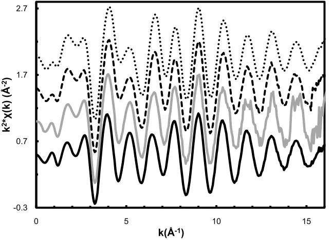
Figure 2-8: x(k) extracted from the µ(E) of as-deposited 6.1%N-GST (black dotted line), 5%N-GST (black dashed line), 2.5%N-GST (gray solid line), and GST (black solid line), using the AUTOBK program. Each spectrum is the average of at least four florescence
measurements. Each x(k) function is multiplied by k2 to emphasize the high-energy oscillations, as shown on the y-axis.
Figure 2-8 shows the spectra extracted from , using the background removal values above. The presence of high k noise in 2.5%N-GST lead us to use ∆k = 3-13
Ǻ-1 for the comparison in figure 2-9. Since EXAFS oscillations rapidly diminish with
-0.3 0.7 1.7 2.7
0 5 10 15
k
2*χ
(k) (Å
-2)
portion of the data. As a rule, all data in this dissertation will be weighted (e.g y-axis label of figure 2-8), and the magnitude of the FT will similarly always reflect this, (e.g y-axis label of figure 2-9).
Figure 2-9: Magnitude of Fourier transformed EXAFS spectra of 6.1%N-GST (black dotted line), 5%N-GST (black dashed line), 2.5%N-GST (gray solid line), and 2.5%N-GST (black solid line), using a window range of ∆k = 3-13.5 Ǻ-1. The gray line shows the background feature.
Figure 2-9 is the magnitude of the complex FT of , that is | |, for these data sets. At ~1.1Å, in all cases, there is a split shell which can be misleading. Indeed, if the feature at ~1.1Å was structure related to surface oxide or impurities on the substrate prior to deposition (which may form an unknown Ge interfacial layer), we would not expect it to increase in proportion to Ge-N bonding feature as observed. This is not a real feature, but rather FEFF’s (specifically, AUTOBK) difficulty in defining a background function in the near edge-region of the spectra, where the absorption spectrum changes abruptly and beyond the flexibility of a spline. An appropriate cutoff is needed here to exclude the Fourier
0 0.4 0.8 1.2
0 1 2 3 4
|
χ
(R)| (Å
-3)
components that are longer in wavelength than that in the Ge-N EXAFS structure [69] by setting a maximum Rbkg, below which contributing Fourier components are considered to be
part of the background. For our N-GST data, Rbkg =1.0Å (figure 2-7) was used, since higher
values seemed to remove both the background as well as part of the EXAFS data. For completeness, we show the typically ignored surface oxide in the undoped sample, and thus any resemblance to the Ge-N related spectra in the doped samples is coincidental. “Typically ignored” means that this surface oxide may actually be any number of impurities (plus
oxygen), and it’s amplitude is usually just above the background noise level: it usually disappears completely after background subtraction. However, in this case depth profile XPS implies that it is mainly germanium oxide, so we can retain it for fitting. The location of the arrows in figure 2-9 indicated a Ge-N and Ge-N-Ge feature, clearly separate from the amorphous GST structure [70]: the local structure of amorphous GST bonds appeared unperturbed by nitrogen addition.
captured in in the sine term in the EXAFS (Eqn 2.2). This is seen in figure 2-9, where the first shell bond lengths are shifted to a distance of 1.5Å. Second, MS paths of the
photoelectron can produce strong signals in the FT of the EXAFS and are not part of a RDF. Third, unlike an RDF, the interference between two scattering paths of the photoelectron may result in a minimum rather than a peak in the FT of the EXAFS data. Fourth, the amplitude of the peaks in the FT of the EXAFS data depends on many EXAFS variables (Eq. 2.2). For instance, causes the EXAFS amplitude to diminish with increasing radial distance. The amplitude of a RDF depends only on the coordination number (N).
specific scattering shells of a FT can be isolated for analysis and fitting, however this was not done for any of our data sets.
2.5.3 EXAFS Models and Fitting
The similarities between the vibrational spectra and Ge near edge spectra of N-GST versus other amorphous and crystalline germanium nitrides, will direct our models for quantitative EXAFS analysis. The strong absorption in FTIR at ~700 cm-1 is consistent with a Ge-N bonding, where we observed the dominant asymmetric stretching mode associated with the Ge3N skeletal group. The N atomic configuration, 1s2s2px2py2pz, can complete its
valence shell by a) electron gain to form the nitride ion ; b) strong covalent bonds (single or multiple), like in molecular ; c) other covalent bonds from electron gain, as in ; d) electron-pair bonds with electron loss, as in tetrahedral ammonium [71]. molecules are pyramidal; the bonding involves sp3 orbitals so that the lone pair occupies the fourth position. Electronic studies of amorphous and crystalline germanium [72] and silicon [73; 74] nitrides reveal that nitrogen bonds to both Ge and Si in a similar, unique, pyramidal configuration which has been described as sp2 hybridization [75]. In this structure, Ge (or Si)
Ge(1-x)Nx nitrides [62] and main electronic features between amorphous Si and Ge nitrides are
the same [72; 77].
Consequently, we used the ATOMS interface in IFEFFIT to generate a list of atomic co-ordinates about the Ge absorber, based on: A) the distorted tetrahedral unit cell parameters from β-Ge3N4 [63] as well as B) the simple first shell tetrahedral bonded Ge-Ge, Ge-Te, and
Ge-Sb. Typically for amorphous samples and mixed systems, it is a known technique in EXAFS modeling to use mixing variables to calculate the bonding fraction of each unique environment [78]. Therefore, we have (Ge-N paths)*x + (Ge-Ge)*y Sb)*z +(Ge-Te)*(1-x-y-z), where 0 , , 1. The ATOMS output is a theoretical FEFF calculation, each with paths which can be arbitrarily chosen for fitting by the user. Once a path has been selected and added for testing, the remaining math expressions for the path variables (from the EXAFS equation) were constrained as follows:
• ∆R – The change in path length was determined independently for each path in the GST environment, ie, Ge-Ge, Ge-Te, and Ge-Sb. ∆R values were constrained to be the same for all paths in the Ge-N 1st shell, while all Ge-N-Ge paths in the second shell also had one ∆R variable .
• σ2 – Coordination shells with similar atoms and bond distance were constrained to have the same debye waller factors. For instance, all Ge-N-Ge paths, for all data sets utilized just a single σ2 variable.
• N – The path degeneracy for the Ge-N and Ge-N-Ge paths were determined from the β -Ge3N4 crystal structure. For the GST related paths, we followed the 8-N rule, and N was
constrained to 4.
• So2– One value of the amplitude reduction factor was used for each sample, and this was
restrained to be close to fitted values of known Ge references standards measured at each run, since it is mostly chemically transferable [52]. We set S02 = 0.80 for all N-GST
samples.
Each N-GST sample was imported into the Artemis project, creating 4 unique data sets, and multiple data sets (MDS) was employed. MDS is the simultaneous calculation of best fits to the theoretical paths for more than one N-GST sample (data set) at a time. For instance, it was reasonable to assume that the Ge-N and Ge-N-Ge bond lengths were similar for all N-GST Ge environments. We can easily implement this constraint using MDS fitting, to obtain a better measure of the parameterized path parameters and significantly reduce the number of variables that must be determined in our fits, thus improving the statistical
significance of the results. Multiple k-weight (MKW) fitting, using kw=1, 2, and 3, was done in all cases. Since different parameters effect different regions of data, MKW allows us to distribute the importance of the evaluation of the chi-square over the entire k range.
number of variables,
N
var, which must be less than Nind, theχ
2 (chi-square),χ
2v (reducedchi-square), and the R factor. The important considerations of these standard goodness-of-fit statistical parameters for EXAFS analysis are covered in by Stern et al. [79], but the
highlights are:
R factor – The R factor is the sum of the squares of the differences between the data and the fit at each data point, divided by the sum of the squares of the data at each corresponding point. It represents the mean square misfit between the data and the fit for both the real and imaginary parts of the Fourier transform and it is defined as:
∑
∑ [Eqn. 2.5]
In general, fits with R factor values ≤ 0.05 are considered reasonably good.
χ
2 – Theχ
2 value is the sum of the squares of the difference between the predicted fit and thedata divided by the uncertainties (
ε
) at each data point (i
). It is calculated as:∑ [Eqn. 2.6]
The sum is over each data point in the real and imaginary parts of the Fourier transform, Nind
is the number of independent points in the model fit, and Npts is the number of data points.