Square Patch-Based Dielectric Microwave Absorber
Amit Bhati1, *, Kirankumar R. Hiremath1, and Vivek Dixit2
Abstract—The work presents a simple and novel design approach to extend the bandwidth of existing Dielectric Material Based Microwave Absorber (DMBMA). The design comprises planar square patches of DMBMA placed periodically on a metalbacked FR4 sheet. For demonstration purpose, the DMBMA is synthesized by adding conducting carbon fillers in polyurethane matrix, and its electromagnetic parameters are measured in X-band. A single reflection null is observed in DMBMA owing to λ/4 resonance. In comparison, the bandwidth of 8 GHz (10–18 GHz) is achieved for −10 dB reflection for square patch based DMBMA. The thickness of proposed absorber is 2.75 mm. An additional resonant mode is observed due to capacitive coupling between the square patches. The enhanced bandwidth is attributed to the overlapping ofλ/4 resonance and induced coupling mode. A good agreement between the simulated and measured data is observed.
1. INTRODUCTION
Electromagnetic absorbers find a wide range of applications in modern defence systems, commercial and civil sectors. Microwave absorbers are widely employed for reducing electromagnetic interference between the circuit components, improving antenna radiation pattern and radar signature suppression [1]. The practical application considerations necessitate that the absorbers should have lightweight, low thickness, wide band and nearly perfect absorption characteristics [2]. The classical microwave absorbers viz. Salisbury and Jaumann absorbers suffer from disadvantages of narrow bandwidth and large size, respectively [3, 4]. These disadvantages can be minimized using material based microwave absorbers. The material based absorbers are physically realized as composites of conducting fillers in epoxy matrix [2]. However, the practical applications of such absorbers are restricted due to the limited tailoring of constitutive parameters and thickness [5]. In this context, Metamaterial Absorbers (MAs) offer novel features such as low thickness, nearly perfect absorption and flexibility for tuning of resonant frequency [6]. However, the MAs have disadvantages such as narrow bandwidth owing to the formation of resonating structure, and polarization conversion due to the absence of resistive components [6, 7].
Considering the limitations of classical, material and metamaterial absorbers, an inventive design approach is essential to improve the bandwidth of existing microwave absorbers. In this work, a simple design methodology is proposed and validated, which extends the bandwidth of the available DMBMA significantly. It is noted from the reported literature that additional resonant modes are introduced for improving the bandwidth of the absorbers viz. by incorporating frequency-selective surface (FSS) and multilayer absorber [8, 9]. In the present work, the additional resonance is induced using the square patches of DMBMA. The selective overlapping of λ/4 and the induced additional resonance result in bandwidth enhancement of DMBMA.
The composite of conducting carbon in polyurethane matrix is synthesized to support the design of the absorber. The permittivity and permeability of composite are measured in X-band. The measured
Received 24 September 2017, Accepted 17 November 2017, Scheduled 30 November 2017
* Corresponding author: Amit Bhati ([email protected]).
EM material parameters are compared with the control sample. The square patches of the composite are placed periodically on a metal backed FR4 sheet. The simulated and measured reflection from the absorber indicates the bandwidth of 8 GHz for −10 dB reflection. The total thickness of the proposed absorber is 2.75 mm. The absorbance mechanism in the designed absorber is illustrated using field quantities and parametric analysis of geometric parameters.
2. DESIGN AND RESULTS
2.1. Synthesis of Dielectric Absorber
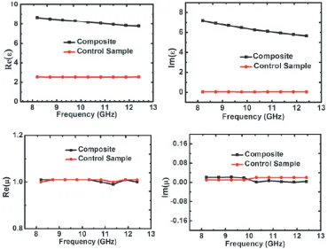
The purpose of synthesizing DMBMA is to practically demonstrate the origin of additional resonance due to coupling between the square patches. The detailed discussion regarding the design, analysis and physical realization of desired material parameters are reported in [2, 5, 10–13]. The interaction of EM waves with the material is characterized by its constitutive parameters viz. permittivity and permeability. The EM material’s real and imaginary parameters are related by Kramers-Kronig relations [5]. Owing to its dependence, the arbitrary values cannot be considered. Due to Snoek’s limit [5], light weight and ease of synthesis, the dielectric absorber is considered. The dielectric absorbers are characterized by its real and imaginary parts of permittivity due to non-magnetic response. The dielectric absorber is synthesized by adding 6% w/w conducting carbon in a polyurethane matrix. Homogenous dispersion of the filler in polyurethane matrix is carried out using ball milling process, a widely used technique in material synthesis [21]. The material parameters of the control sample (polyurethane resin) and composite (carbon filler in polyurethane matrix) are measured in X-band using waveguide method. The measured permittivity and permeability of the synthesized composite are shown in Fig. 1. It is noted that by adding conducting filler in a polyurethane matrix, the material parameters can be tuned. Owing to dielectric nature of the filler, the permittivity values of the composite change significantly whereas the permeability values remain almost invariant.
The S-parameters of designed absorbers are simulated in CST Microwave Studio using frequency
domain solver under unit cell boundary conditions. The material parameters as presented in Fig. 1 are plugged in the material dispersive list of CST Microwave Studio and fitted with 2nd order. The absorbance of metal backed absorber is calculated using the relation A(ω) = 1−R(ω) = 1− |S11|2.
By minimizing the reflectance, the absorbance can be enhanced. The performance of the absorber is simulated for different polarization angles and oblique incidence for TE and TM components.
2.2. Design of Dielectric Absorber
The impedance and return loss of material based absorber are expressed as [2]:
Zd = Z0
μ ε tanh
−
j2πf d√με c
(1)
RL(dB) = 20log10Zd−Z0
Zd+Z0
(2)
where Zd, Z0, f, d, ε, μ and c are the material impedance, free space impedance, frequency, thickness,
permittivity, permeability and speed of light, respectively. The material impedance can be tailored by permittivity, permeability and thickness. For quarter wavelength thickness, the absorber forms an open transmission line which results in reflection null because of impedance matching condition [1].
The DMBMA is composed of a layered arrangement of, bottom to top, metal sheet, FR4 sheet and synthesized composite, as shown in Fig. 2(a). The utility of FR4 spacer is discussed in Section 4. The permittivity and dielectric loss tangent of FR4 are 4.2 and 0.02 respectively. The thickness of the FR4 sheet and dielectric absorber are referred as tf r= 1 mm and d= 1.75 mm, respectively.
(a)
(b)
Figure 2. (a) Side view of the dielectric absorber. (b) Simulated reflection of synthesized dielectric absorber for different dvalues andtf r=1 mm.
The simulated return loss of synthesized absorber is depicted in Fig. 2(b) for different values of d
and tf r= 1 mm. For the dielectric absorber, a single mode is observed due toλ/4 resonance (whereλ
is the wavelength in the medium) [14]. The resonant peak shifts towards lower frequency region as the dielectric absorber’s thickness increases.
2.3. Design of Square Patch DMBMA
angle Φ simultaneously with respect toyandxdirection respectively. The performance of the absorber is almost invariant due to four-fold rotational symmetry as shown in Fig. 3(d) [22, 23].
It is noted that for frequency region 10 GHz to 18 GHz the reflection is below −10 dB with a bandwidth of 8 GHz (Fig. 3(d)). The two reflection nulls are observed at 12 GHz and 16 GHz. The parametric analysis of geometric parameters indicate the null at 12 GHz mainly arises fromλ/4 resonance whereas the null at 16 GHz originates due to the coupling between the square patches. Fig. 3(e) presents the orientation of the wave vector, electric field and magnetic field for oblique incidence under TM mode. The magnetic field is aligned in x direction whereas the wave vector and electric field are changed simultaneously by an angleθwith respect tozand ydirection respectively [24]. The results for oblique incidence 0◦ to 60◦ under TM mode are plotted in Fig. 3(f). Fig. 3(g) shows the orientation of the wave vector, electric field and magnetic field for oblique incidence under TE mode. The electric field is aligned in y direction whereas the wave vector and magnetic field are changed simultaneously by an angle θ with respect to z and x direction respectively [24]. The results for oblique incidence 0◦ to 60◦ under TE mode are plotted as Fig. 3(h). The performance of the absorber for−10 dB reflection is almost stable up to 30◦ for oblique incidence under TE and TM mode respectively.
(a)
(b)
(c) (d)
(g) (h)
Figure 3. (a) & (b) Side and top views respectively, of the absorber along with wave vector, electric and magnetic field for p = 12 mm, a= 10 mm, d= 1.75 mm and tf r = 1 mm. (c) Orientation of the wave vector, electric field and magnetic field for different polarization angles. (d) Simulated results for polarization angles 0◦ to 45◦. (e) Orientation of the wave vector, electric field and magnetic field for oblique incidence under TM mode. (f) Simulated results for oblique incidence 0◦ to 60◦ under TM mode. (g) Orientation of the wave vector, electric field and magnetic field for oblique incidence under TE mode and (h) Simulated results under TE mode for oblique incidence 0◦ to 60◦.
3. ANALYSIS AND DISCUSSION 3.1. Effect of Square Patch Size
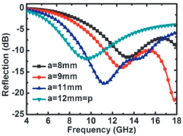
The simulated reflection for different square patch sizes is plotted in Fig. 4. It is evident that for
a= 12 mm =p, the single resonant mode is observed at 9 GHz due to λ/4 resonance. For a= 11 mm, two reflection nulls are noted at 11 GHz and 15 GHz. The decrease in patch size shifts the reflection dip to the higher frequency region. It is also noted that the nulls are well separated as the patch size decreases. For a = 10 mm the nulls are well overlapped and result in 8 GHz bandwidth for −10 dB reflection (Fig. 3(d)).
Figure 4. Simulated reflection for different square patch sizes (d= 1.75 mm and tf r= 1 mm).
The origin of the additional null is attributed to the formation of capacitance between the edges of square patches [15]. The strength of the coupling is dependent on the size and spacing of the square patch for the given dielectric material [15]. As the spacing between the patches is decreased, the coupling null shifts to lower frequency due to the increased coupling strength. The increase in spacing leads the coupling null shifts towards higher frequency due to the decrease in coupling strength. For
observed in DMBMA. It is noted that as the square patch size decreases the λ/4 resonance shifts to a higher frequency. The square patches decrease the material impedance which shifts the absorbance peak to a higher frequency [16].
3.2. Physical Insight
The field quantities are numerically estimated to support the claim regarding the origin of the additional absorbing peak. The field quantities are estimated for d = 1.75 mm, p = 12 mm, a = 10 mm and
tf r= 1 mm at absorbing frequencies 12 GHz and 16 GHz (Fig. 5).
(a) (b)
(c) (d)
Figure 5. Simulated electric field and power loss distribution at absorbing frequencies 12 GHz and 16 GHz respectively. (a) Electric Field 12 GHz. (b) Electric Field 16 GHz. (c) Power loss 12 GHz. (d) Power loss 16 GHz.
4. FABRICATION AND EXPERIMENTAL RESULTS 4.1. Dielectric Absorber
The synthesized DMBMA is shown in Fig. 6(a) with dimensions 115 mm×115 mm×2.75 mm. The
λ/4 resonance absorption peak of the synthesized dielectric absorber is at approximately 16.1 GHz for
d= 1.75 mm. The FR4 spacer is used to increase the thickness of the synthesized absorber to measure the reflection in 3–18 GHz range. The representative measurement setup is depicted in Fig. 6(b). The reflection measurement of designed absorbers is carried out in an anechoic chamber using Vector Network Analyzer (VNA) and a pair of horn antennas as described in [17, 18] The experimental and simulated reflection of the synthesized absorber are shown in Fig. 6(c). The deviation in the results is attributed to fabrication and experimental errors.
(a) (b) (c)
Figure 6. (a) Synthesized dielectric absorber. (b) Schematic of measurement setup. (c) Simulated and measured reflection of dielectric absorber.
4.2. Square Patch Dielectric Absorber
The designed absorber is physically realized by cutting square patches of the synthesized dielectric absorber of dimensions 10 mm×10 mm. The square patches are placed manually, on a metal backed FR4 sheet with a periodicity of 12 mm using an epoxy-based adhesive. The fabricated absorber, having the dimensions 120 mm×120 mm ×2.75 mm, is shown in Fig. 7(a). The simulated and measured results are shown in Fig. 7(b). A good agreement between the measured and simulated results validate the design of the absorber. The slight deviation is attributed to the variation of spacing between the square patches due to manual alignment (Fig. 7(a)). The experimental results indicate the bandwidth of 8 GHz for −10 dB reflection. The reflection from the absorber is measured for varying aspect angles at different frequencies and compared with the metal sheet. The aspect angle is the angular orientation of the absorber with respect to the antennas where the position of the antennas are remain fixed [25].
(d) (e) (f)
Figure 7. (a) Fabricated square patch based dielectric absorber. (b) Simulated and experimental results for square patch based dielectric absorber. (c) to (f) Measured reflection from metal and absorber for varied aspect angle at different frequencies.
The reflection from the absorber is less in comparison to the metal as shown in Fig. 7 ((c) to (f)). For the given aspect angle, the difference between the metal and absorber reflection gives the absorbance of the absorber. The performance of the absorber is stable for the small aspect angle. The low angular stability is attributed to small permittivity values of the synthesized DMBMA [19, 20]. The angular stability of the absorber can be improved by increasing the real part of permittivity.
5. CONCLUSION
The work suggests a simple and implementable design approach to improve the bandwidth of available DMBMA. The bandwidth improvement is attributed to simultaneously overlapping of λ/4 mode and an additional induced mode due to capacitive coupling between the square patches of DMBMA. The bandwidth of DMBMA can be further improved by designing the unit cell consisting of square patches of different DMBMA with varied thickness. The designed absorber finds a wide range of applications in civil, commercial and defence sectors.
ACKNOWLEDGMENT
The first author is grateful to the Director, Defence Laboratory, Jodhpur, Rajasthan, India for kind permission to carrying out the research work. The authors are thankful to Mr. R. K. Jani, Mr. V. S. Chauhan and Mr. Umesh Kumar of Defence Laboratory, Jodhpur, for their kind support in the characterization of the absorbers. The valuable suggestions of Dr Abhinandan Jain of Defence Laboratory, Jodhpur for synthesising dielectric absorber are acknowledged.
REFERENCES
1. Watts, C. M., X. Liu, and W. J. Padilla, “Metamaterial electromagnetic wave absorbers,” Adv. Mater., 24, 2012.
2. Qin, F. and C. Brosseau, “A review and analysis of microwave absorption in polymer composites filled with carbonaceous particles,” Journal of Applied Physics, Vol. 111, 061301, 2012.
3. Fante, R. L. and M. T. McCormack, “Reflection properties of the salisbury screen,” IEEE Transactions on Antennas and Propagation, Vol. 36, No. 10, 1988.
4. Saville, P., Review of Radar Absorbing Materials, Defence Research & Development Atlantic Dartmouth, Canada, 2005.
5. Rozanov, K. N., “Ultimate thickness to bandwidth ratio of radar absorbers,” IEEE Transactions on Antennas and Propagation, Vol. 48, No. 8, 1230–4, 2000.
7. Kundu, D., A. Mohan, and A. Chakraborty, “Comment on ‘Wide-angle broadband microwave metamaterial absorber with octave bandwidth’,” IET Microwaves, Antennas Propag., Vol. 11, No. 3, 442–443, 2017.
8. Panwar, R., S. Puthucheri, V. Agarwala, and D. Singh, “Fractal frequency-selective surface embedded thin broadband microwave absorber coatings using heterogeneous composites,” IEEE Transactions on Microwave Theory and Techniques, Vol. 63, No. 8, 2438–2448, 2015.
9. Noor, A. and Z. Hu, “Wideband multilayer Sierpinski carpet array radar absorber,” Electronics Letters, Vol. 52, No. 19, 1617–1618, 2016.
10. Brosseau, C., P. Qu´eff´elec, and P. Talbot, “Microwave characterization of filled polymer,”Journal of Applied Physics, Vol. 89, 2001.
11. Tuncer, E., Y. V. Serdyuk, and S. M. Gubanski, “Dielectric mixtures: Electrical properties and modeling,” IEEE Transactions on Dielectrics and Electrical Insulation, Vol. 9, No. 5, 809–828, 2002.
12. Cheng, E. M., M. F. Malek, M. Ahmed, K. Y. You, K. Y. Lee, and H. Nornikman, “The use of dielectric mixture equations to analyze the dielectric properties of a mixture of rubber tire dust and rice husks in a microwave absorber,”Progress In Electromagnetics Research, Vol. 129, 559–578, 2012.
13. Koledintseva, M. Y., R. E. DuBroff, and R. W. Schwartz, “A Maxwell Garnett model for dielectric mixtures containing conducting particles at optical frequencies,” Progress In Electromagnetics Research, Vol. 63, 223–242, 2006.
14. Wang, B., J. Wei, Y. Yang, T. Wang, and F. Li, “Investigation on peak frequency of the microwave absorption for carbonyl iron/epoxy resin composite,” Journal of Magnetism and Magnetic Materials, Vol. 323, No. 8, 1101–1103, 2011.
15. Luukkonen, O., F. Costa, C. R. Simovski, A. Monorchio, and S. A. Tretyakov, “A thin electromagnetic absorber for wide incidence angles and both polarizations,” IEEE Transactions on Antennas and Propagation, Vol. 57, No. 10, 3119–3125, 2009.
16. Costa, F., A. Monorchio, and G. Manara, “Analysis and design of ultra thin electromagnetic absorbers comprising resistively loaded high impedance surfaces,”IEEE Transactions on Antennas and Propagation, Vol. 58, No. 5, 1551–1558, 2010.
17. Cheng, Y. and H. Yang, “Design, simulation, and measurement of metamaterial absorber,”Journal of Applied Physics, Vol. 108, 034906, 2010.
18. Li, M., H. L. Yang, X. W. Hou, Y. Tian, and D. Y. Hou, “Perfect metamaterial absorber with dual bands,”Progress In Electromagnetics Research, Vol. 108, 37–49, 2010.
19. Costa, F., S. Genovesi, A. Monorchio, and G. Manara, “A circuit-based model for the interpretation of perfect metamaterial absorbers,” IEEE Transactions on Antennas and Propagation, Vol. 61, No. 3, 1201–1209, 2013.
20. Chambers, B., “Optimum design of a Salisbury screen radar absorber,”Electronics Letters, Vol. 30, No. 16, 1353–1354, 1994.
21. Suryanarayan, C., “Mechanical alloying and milling,”Progress in Materials Science, Vol. 46, No. 1, 1–184, 2001.
22. Zhu, B., Z. Wang, C. Huang, Y. Feng, J. Zhao, and T. Jiang, “Polarization insensitive metamaterial absorber with wide incident angle,”Progress In Electromagnetics Research, Vol. 101, 231–239, 2010. 23. Lu, L., S. Qu, H. Ma, F. Yu, S. Xia, Z. Xu, and P. Bai, “A polarization-independent wide-angle dual directional absorption metamaterial absorber,”Progress In Electromagnetics Research M, Vol. 27, 91–201, 2012.
24. Bhattacharyya, S., “A broadband microwave metamaterial absorber with octave bandwidth,”
Mapan, 299–307, 2016.