High-Speed and Energy-Efficient Energy Efficient Carry Skip
Adder Using Skip Logic
Anitha Banoth
Department of ECE, CITS, Warangal, Telangana
Email id: [email protected]
Abstract— here we present a carry skip adder (CSKA) structure has a higher speed but lower energy consumption with compared to conventional. The speed enhancement is applying by achieved incrementation and concatenation schemes to efficiency of the conventional CSKA (Conv-CSKA) structure. In addition, utilizing instead of multiplexer logic, the proposed structure makes use of OR-AND-Invert (OAI) and AND-OR-Invert (AOI) compound skip logic gates. The structure may be realized with both variable stage size styles and fixed stage size, where in the latter improves further the energy and speed parameters for the adder. Finally, a variable hybrid latency extension of the proposed model, which Reduces power consumption considerably without impacting the speed, is presented. This utilizes extension a modified structure for parallel in increasing the slack time, and hence, enabling voltage further reduction. The proposed structures by comparing are assessed their speed, power, and with energy parameters those of other using a adders 45-nm static CMOS technology for a of supply voltages wide range. The results that are using HSPICE obtained simulations reveal, on average, 44% and 38% improvements in the delay and energy, respectively, compared with those of the Conv-CSKA. In addition, the power–delay product was the lowest the structures among considered in this paper, while its product was almost energy–delay the same as that of the Kogge–Stone prefix adder parallel with considerably area and power consumption low. Simulations on the variable latency proposed hybrid CSKA reveal reduction in the compared with the power consumption latest works in this field while high speed having a reasonably.
I. INTRODUCTION
ADDERS are a key in arithmetic building block and logic units (ALUs) [1] their speed and reducing their power/energy consumption strongly hence increasing affect the power consumption and speed of processors. There are many works on the subject of the speed and optimizing power of these units, which have in [2]–[9]. Obviously, it is been reported highly desirable to speeds at achieve higher low- consumptions power/energy, which is a challenge for the designers of processors of general purpose. Low circuits power arithmetic have become very important in VLSI industry. Due to the of portable electronic component, Adder circuit rapid growth is the main building block in DSP processor.
Adder in the arithmetic unit main component. A Complex DSP several adders. are forced system involves with are high speed , high throughput more constraints, The Designers small silicon area and low power consumption. Many design styles of adders exist .Although, Ripple carry adders are the small in design structure but its very slower. Most recently, carry-skip adders [1, 2, 3] are due to their performance of small size high speed used popularly. Generally, in an N-bit carry-skip adder divided into M-bit number of blocks [1, 4], a long-range of carry signal starts at a block Bi, which some bits in that
block, then some blocks rippling it skips through, and ends with a block Bj. Carry-look-ahead and carry-select but far larger and consume much more very fast power than ripple or adders are carry-skip adders. Into appropriate both Lynch-Swartzlander
Two of the fastest known addition circuits are the. They are based on the usage of a carry tree that produces carries bit positions without back propagation. In order to obtain the valid sum bits as soon as possible, in and Kantabutra’s adders the sum bits are computed by means of perform carry-select blocks, which are able to their operations in parallel with the Recently carry-tree, the near-threshold region has been considered as a provides a more desirable tradeoff point between delay and power dissipation compared with that of the sub threshold one, because it results in region that lower delay compared with the sub threshold region and significantly and leakage lowers switching powers compared with the superthreshold
region.
circuits with the feature of dynamic the motivation voltage and frequency scaling. In these circuits, to reduce the energy consumption, the system may voltage change (and frequency) of the circuit based on the requirement workload. For these systems, the circuit to operate under a should be able wide range of supply voltage levels. of course, achieving at lower supply higher speeds voltages for the computational blocks, with the adder as one main components, could be crucial in the, yet energy efficient, processors. Design of high-speed In this paper, given the features of the attractive CSKA structure, we have focused on reducing its delay by modifying its implementation based on the static CMOS logic.
The concentration on the static CMOS originates from the desire to have a reliably operating circuit under a wide range of supply voltages in highly scaled technologies [10]. The proposed modification increases the speed considerably while maintaining the low area and power consumption features of the CSKA. In addition, an adjustment of the structure, based on the variable latency technique, which in turn lowers the power consumption without considerably impacting the CSKA speed, is also presented. To the best of our knowledge, no work concentrating on
design of CSKAs operating from the superthres hold region down to near-threshold region and also, the design of (hybrid) variable latency CSKA structures have Been reported in the literature.
II. PRIOR WORK
Modifying CSKAs for Improving Speed
Alioto and Palumbo [19] propose a simple strategy for the design of a single-level CSKA. The method is based on the VSS technique where the near-optimal numbers of the FAs are determined based on the skip time (delay of the multiplexer), and the ripple time (the time required by a carry to ripple through a FA). The goal of this method is to decrease the critical path delay by considering a non integer ratio of the skip time to the ripple time on contrary to most of the previous works, which considered an integer ratio [17], [20]. In all of the works reviewed so far, the focus was on the speed, while the power consumption and area usage of the CSKAs were not considered. Even for the speed, the delay of skip logics, which are based on multiplexers and form a large part of the adder critical path delay [19], has not been reduced.
Improving Efficiency of Adders at Low Supply Voltages
To improve the performance of the adder structures at levels, some methods have been proposed low supply voltage in . In adaptive clock stretching operation has. The method is based on the observation that the critical paths in adder units are rarely activated. Therefore, been suggested the slack time between the critical paths and the off-critical paths may be used to reduce the supply
voltage. reduction must not increase Notice that the voltage the delays of the noncritical timing paths to become larger than clock allowing the period of the us to keep the original clock frequency at a reduced supply voltage level. Timing paths in the are When
clock cycles to complete the operation. This way the power consumption reduces considerably at the cost of rather small throughput degradation
In the proposed hybrid structure, the KSA has been used in the middle part of the C2SLA where
This leads to the positive combination slack time increase. However, and its hybrid version the C2SLA are not good candidates for low-power ALUs. This from the fact statement originates that due to the logic duplication in this type of adders, the power consumption and also the PDP are still high even at low supply voltages The CSKA may be implemented using FSS and VSS Where the highest speed for the VSS structure .Here, the stage size is the same as the RCA block size. In Sections III-A and III-B, these two different implementations of may be obtained the CSKA adder are described in more detail.
III PROPOSED CSKA STRUCTURE
The structure is based on combining the concatenation and the incrementation schemes [13] with the structure, and hence Conv-CSKA, is denoted by CI-CSKA. It provides us with the ability to use
simpler carry skip replaces logics. 2:1 multiplexers by AOI/OAI compound gates (Fig. 2). The gates, which consist of fewer transistors, have lower delay, area, and smaller power consumption The logic compared with those of the 2:1 multiplexer [37]. Note that, in this structure, as
The through the skip logics, it becomes carry propagates complemented. Therefore, at the output of the skip logic of, the complement of the carry is generated. The structure has a even stages considerable lower propagation delay with a slightly smaller area compared with those of the conventional one. Note that while the AOI (or OAI) gate is smaller than that of the power consumptions multiplexer, the power consumption of the proposed CI-CSKA is a little more conventional one
than that of the. This is due to the the number of the gates, which imposes a higher wiring increase in capacitance (in the noncritical paths).
The reason for using both OAI and AOI compound gates as is the inverting functions of these the skip logics gates in standard cell libraries. This way the need for an inverter gate, the power consumption which increases and delay, is eliminated. As shown in Fig. 2, if an AOI is used skip logic, the next skip logic should use OAI gate. In addition, to mention is that the use of the another point proposed skipping structure in the Conv-CSKA structure the delay of the critical path increases considerably. This originates from the fact that, in –CSKA the Conv, the skip logic is not able to bypass the zero carry input until the zero carry propagates input from the corresponding RCA block.
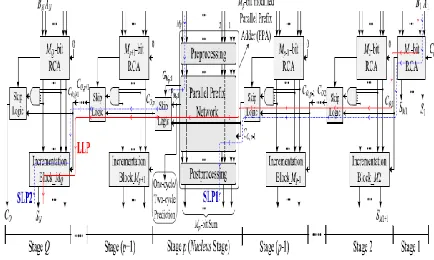
4. Proposed Hybrid Variable Latency CSKA Structure
Fig-4: Structure of the proposed hybrid variable latency CSKA
In the proposed hybrid structure, the prefix network of the Kogge-Stone adder is used for constructing the nucleus stage (Fig-5). One the advantages of this adder compared with other prefix adders is less fan-out of adder, while the length of its wiring is smaller. Finally, it has a simple and regular layout. The internal structure of the stage p, including the modified PPA and skip logic, is shown in Fig- 5. Note that, for this figure, the size of the PPA is assumed to be 8 (i.e., Mp = 8).
IV RESULTS
Block diagram
The design proposed in this paper has been developed using MODEL SIMULATOR. ADDERS are the main building block in ALUs. Low power arithmetic circuits have become important in VLSI industry. Adder circuit is the main building block in
DSP processor. Adder is the main component of arithmetic unit process. A complex DSP system involves adders. Many design styles of adders exist.
Fig 3 Simulation results
V. CONCLUSION
In this paper, a static CMOS CSKA structure called CI-CSKA was which exhibits a higher speed proposed, lower energy consumption compared with those of the conventional. The speed was achieved by modifying the enhancement structure through the incrementation and concatenation techniques. In addition, AOI and OAI compound gates were exploited for the carry skip logics. The efficiency of the proposed structure for VSS and FSS was studied by comparing its power and delay with those of the Conv-CSKA, CIA, RCA, SQRT-CSLA, and KSA structures. The results revealed considerably lower PDP for the VSS implementation of the CI-CSKA structure over a voltage from wide range super-threshold to near super-threshold. The results also suggested the CI-CSKA structure as a adder for the very good applications where both the speed and energy consumption is good. In addition, a hybrid variable latency extension of the was proposed. It exploited a structure modified parallel adder structure at the middle stage for increasing the slack time, which provided us with the opportunity for lowering the supply voltage. The efficacy energy consumption of this structure was compared by reducing versus those of the variable latency RCA, C2SLA, and hybrid C2SLA structures.
Again, the suggested structure showed the lowest PDP delay and making itself as candidate for low-energy and high-speed applications.
[1] I. Koren, Computer Arithmetic Algorithms, 2nd ed. Natick, MA, USA: A K Peters, Ltd., 2002. [2] R. Zlatanovici, S. Kao, and B. Nikolic, ―Energy– delay optimization of 64-bit carry-lookahead adders with a 240 ps 90 nm CMOS design example,‖ IEEE J. Solid-State Circuits, vol. 44, no. 2, pp. 569–583, Feb. 2009.
[3] S. K. Mathew, M. A. Anders, B. Bloechel, T. Nguyen, R. K. Krishnamurthy, and S. Borkar, ―A 4-GHz 300-mW 64-bit integer execution ALU with dual supply voltages in 90-nm CMOS,‖
IEEE J. Solid-State Circuits, vol. 40, no. 1, pp. 44– 51, Jan. 2005.
[4] V. G. Oklobdzija, B. R. Zeydel, H. Q. Dao, S. Mathew, and R. Krishnamurthy, ―Comparison of high-performance VLSI adders in the energy-delay space,‖ IEEE Trans. Very Large Scale Integr. (VLSI) Syst., vol. 13, no. 6, pp. 754–758, Jun. 2005.
[5] B. Ramkumar and H. M. Kittur, ―Low-power and area-efficient carry select adder,‖ IEEE Trans. Very Large Scale Integr. (VLSI) Syst., vol. 20, no. 2, pp. 371–375, Feb. 2012.
[6] M. Vratonjic, B. R. Zeydel, and V. G. Oklobdzija, ―Low- and ultra low-power arithmetic units: Design and comparison,‖ in Proc. IEEEInt. Conf. Comput. Design, VLSI Comput. Process. (ICCD), Oct. 2005, pp. 249–252.
[7] C. Nagendra, M. J. Irwin, and R. M. Owens, ―Area-time-power tradeoffs in parallel adders,‖ IEEE Trans. Circuits Syst. II, Analog Digit. Signal