Design Of Encoder And Decoder Using Hybrid Lut/Multiplexer
ABSTRACT: In this paper, a novel architecture of encoder and decoder using high security technique for the VLSI implementation for encoder and decoder using Hybrid MUX/LUT. The pre-defined keys are required for each input for both encryption and decryption that are generated in real-time by the key-scheduler module by expanding the initial secret key and thus used for reducing the amount of storage for buffering. S-boxes are used for the implementation of the S.R, M.C and inverses S.R & M.C shared between encryption and decryption. The round keys needed for each round of the implementation are generated in real-time. The forward and reverse key scheduling is implemented on the same device, thus allowing efficient area minimization. Rather than using logical gates we are using hybrid LUT or MUX for speed of operation. The pipelining is used after each standard round makes fast of operation to enhance the throughput and shift row mix column technique gives high security.
Key words: Hybrid MUX/ LUT, Encoder, Decoder, S-box.
I.INTRODUCTION
In Field Programmable Gate Arrays (FPGAs), Look UP Table (LUT) is the primary logic element used for the realization of combinational logic. A K-input LUT can be able to implement any K-input boolean functions. It is very flexible and generic. Recently, other works investigate the alternative FPGA LE architectures for improving the performance. We proposed the MUXs in FPGA logic blocks which increase the silicon area efficiency and logic density. In early commercial architectures, the MUX based logic blocks for FPGAs have succeeded. Consider 6-input LUT is essentially 64-to-1 MUX and 64 SRAM configuration cell but it can only realize a 4-to-1 MUX.
In this paper we propose a six input LE based on a
MUX4 which can realize a subset
of six-input
Boolean logic functions. A new hybrid
complex logic block (CLB) contains a mixture of MUX4s and 6-LUTs. The proposed MUX4s can efficiently map all the input functions. The main contributions are as follows.1. Two hybrid CLB architectures
(nonfracturable and fracturable) that contain a mixture of MUX4 LEs and the traditional LUTs yielding up to 8% area savings.
2. Mapping techniques called Natural Mux and
Mux Map targeted toward the hybrid CLB architecture that optimize for area, while preserving the original mapping depth.
3. A full post-place-and-route architecture
evaluation with VTR7, and CHS tone benchmarks facilitated by LegUp-HLS, the Verilog-to-Routing project showing impact both area and delay.
II. RELATED WORK
A. MUX4: 4-TO-1 Multiplexer Logic
Element:
The MUX4 LE consists of 4-to-1 MUX with optional contrary on its inputs. A 4-to-1 MUX matches the input pin count of a 6-LUT. Inherently, any two-input Boolean function can easily implement in the MUX4. The two-input functions can be connect to the select lines and the truth table values (logic-1 or logic-0) can be routed to the data inputs.
Alternately, a Shannon decomposition can be performed concerning one of the two variables. That variable can feed a select input. Consider Shannon decomposition about one variable produces the cofactors with atmost two variables. Notice that input inversion on each select input is omitted as this 1
S.A.SUNITHA SREE KONDURU,
2N. NAGESWARA RAO,
3Dr.P.BALA MURALI KRISHNA
1
P.G Student, Dept. of E.C.E , Sri Mittapalli Institute of Technology for women, Thummalapalem Guntur, A.P
2Assistant professor, Dept. of E.C.E, Sri Mittapalli Institute of Technology for women, Thummalapalem Guntur, A.P
3would only serve to permute the four MUX data inputs.
Fig 1. MUX4 LE depicting optional data input inversions.
B. Logic Elements, Fracturability And
Mux4-Based Variants:
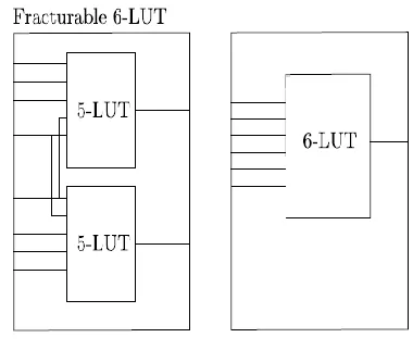
Two families of architectures are produced. They are 1. Without fracturable LEs and 2. With fracturable LEs. The fracturable LEs refer to an architectural element which one or more logic functions can be optionally mapped. Nonfracturable LEs refer to an architectural element on which only one logic function is mapped. We consider an eight-input LE for the fracturable architecture which is closely matched with the adaptive logic module. Fracturable 6-LUT that can be fractured in to two 5-LUTs with shared inputs as shown in below figure.
Fig 2. Fracturable 6-LUT that can be fractured in to two 5-LUTs with shared inputs.
If two inputs are shared between the two functions then two 5-input functions can be mapped into this LE. If no inputs are shared then two four -input functions can be mapped to each 5-LUT. We use two MUX4s within a single eight-input LE. It is shown in the below figure.
Fig 3. Dual MUX LE that utilizes dedicated select inputs and shared data inputs.
The two MUX4s are connected to have dedicated select inputs and shared data inputs. This configuration allows this structure to map two independent three-input functions, while larger functions may be mapped dependent on the shared inputs between both functions.
Examine, an architecture in which a 4-to-1 MUX (MUX4) is fractured into two smaller 2-to-1 MUXs. Since a 2-to-1 MUX‟s mapping flexibility is quite limited. This little benefit was added compared with the overheads of making the MUX4 fracturable and poor area results were observed.
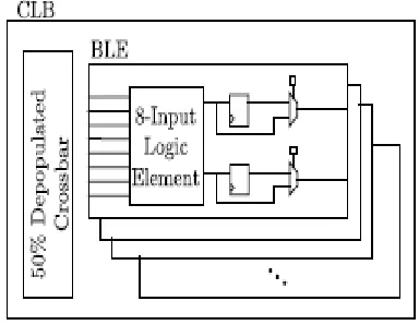
C. Hybrid Complex Logic Block:
A variety of different architectures were considered. In the nonfracturable architecture, the CLB has 40 inputs and ten basic LEs (BLEs), with each BLE having six inputs and one output. Fig. 4 shows this nonfracturable CLB architecture with BLEs that contain an optional register. We vary the ratio of MUX4s to LUTs within the ten element CLB from 1:9 to 5:5 MUX4s:6-LUTs. The MUX4 element is
proposed to work in conjunction with 6-LUTs,
MUX4s Fig. 4 shows the organization of our CLB
and internal BLEs
.
Fig 4. Hybrid CLB with a 50% depopulated intra-CLB crossbar depicting BLE internals for a non fractuable
architecture.
In fracturable architectures, the CLB has 80 inputs and ten BLEs, with each BLE having eight inputs and two outputs. The same sweep of MUX4 to LUT ratios was also performed. Fig. 5 shows the fracturable architecture with eight inputs to each BLE that contains two optional registers. We evaluate fracturability of LEs versus nonfracturable LEs in the context of MUX4 elements since fracturable LUTs
are common in commercial architectures
.
Fig. 5. Hybrid CLB with a 50% depopulated intra-CLB crossbar depicting BLE internals for fracturable architecture.
The crossbars for fracturable architectures are larger than the nonfracturable architectures because of two reasons. Due to the virtual increase of LEs, a larger number of CLB inputs are required, which increases crossbar size. Since there are now twice as many outputs from the LEs, these additional outputs need to also be fed back into the crossbar, also increasing its size. Due to this disparity in crossbar size, fair comparisons cannot be made between fracturable and
nonfracturable architectures. Therefore, we compare nonfracturable hybrid CLB architectures to a baseline LUT only nonfracturable architecture and we compare fracturable hybrid CLB architectures to a
baseline LUT-only fracturable architecture
.
III. Encoder and Decoder Design Using
Proposed MUX
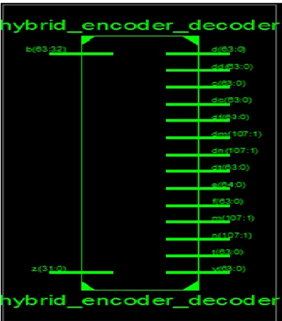
The fig: 6 shows the encoder block diagram with high security implementation. The initial stage having input and initial key to under goes encryption with changing of binary bits into a matrix representation. This conversion of binary data to a matrix is totally carried out by byte sub transformation. Now the total matrix consisting of row and columns by using these we implemented the security by the CLB hybrid crossbar technique.
Fig 6. PROPOSED SYSTEM
another row and with vice and versa. The second technique is mix column transformation it gives two columns into a single column to reduce the size. In another way we can make as comparison of two columns into a single column.
The add round key transformation is used rounding the nearest value of matrix. This represents the rounded output taken as „e‟ for encoder block. The total encoder block is used in the transmitter side. The output of encoder block given to input to decoder block.
Similarly decoder block consisting of sub blocks as encoder with small inversion. So the input „e‟ taken as input for decryption the input „e‟ and final key goes under decryption with CLB hybrid crossbar technique and the output of the decryption given to input as for inverse byte sub transformation. The inverse byte sub transformation divide the matrix representation into binary representation.
IV. RESULTS &
DISCUSSION
The results show that relative to baseline nonfracturable LUT-based LE architectures, the inclusion of hardened MUX4s to form a hybrid LUT/MUX4-based CLB provides an area benefit of up to 8.9% and a 2.5% increase in FMax (for the case of the CHStone circuits, 4:6 architecture and Select
mapping). In essence, this result reaffirms
conventional wisdom that LUTs are in a sense over-engineered for many logic functions that regularly occur in application circuits.
Table 1:Comparision
Existing System
Proposed System
AREA
930
531
%LUT
100%
97%
Table 1 shows the % mux and area in the existing system and proposed system. The fracturable
architectures, overall, show vastly differing
performance compared with the onfracturable architectures.The best architectures are the 1:9 architecture for VTR7 and the 2:8 architecture for CHStone. Only up to 2% area savings are seen for
NaturalMux
mapping
for
fracturable
architectures. The best architectures are the
1:9 architecture for VTR7 but now the 3:7
architecture for CHStone.Fig 7 shows the graphical reprasentation of hybrid lut/mux.Fig 7. COMPARISION
The Hybrid encoder and decoder is designed by using hybrid MUX/Demux. The total input bits of proposed encoder are multiplexed with the initial key by using Hybrid MUX/LUT. After that the encryption and by sub transformation, shift row mix column, add round key will be given to the input and output pins.
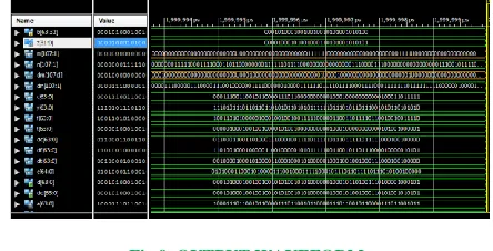
Finally, the DD is the output as shown in the Fig 8
.
Fig 9. OUTPUT WAVEFORM
The Hybrid encoder and decoder are designed by using Hybrid Multiplexer. We have so many operations like separate transformation, shift row, mix column techniques and add round key operation is going on in the internal operations of encoder. Inverse operations of inverse sub transformation, inverse shift row, Inverse mix column and inverse add round key operations are going on at the decoder side. In the Fig 9 shows the inputs of encoder „b,z‟ and „a‟. b,z,a are going on these operations of shift row, mix column and add round key operations of encoder and then gives the output as encoder. This encoder will be transmitted by the transmitter and received by the receiver. Then it is decoder by using the inverse operations of shift row, mix column etc and then gives the output as decoder. This decoder output is equal to the input bits of the transmitter called „b,z‟. The output waveform shown in this figure consisting of inputs b and z. „e‟ encoder is a encoder bit as encoded output. b,z and a are undergoes the encoding technique and gives the encoder output. This encoded output is going on the inverse operation of encoder and then gives the „d‟ decoder. The decoder bits are equal to the b,z as shown in the figure of the output.
V.CONCLUSION
A novel architecture of encoder and decoder using high security technique for the VLSI implementation for encoder and decoder using Hybrid MUX/LUT. The pre-defined keys are required for each input for both encryption and decryption that are generated in real-time by the key-scheduler module by expanding the initial secret key and thus used for reducing the amount of storage for buffering. S-boxes are used for the implementation of the S.R, M.C and inverses S.R & M.C shared between encryption and decryption. The round keys needed for each round of the implementation are generated in real-time. The forward and reverse key scheduling is implemented on the same device, thus allowing efficient area
minimization. Rather than using logical gates we are using hybrid LUT or MUX for speed of operation.
VI.REFERENCES
[1] J. Rose et al., “The VTR project: Architecture and CAD for FPGAs from verilog to routing,” in Proc.
ACM/SIGDA FPGA, 2012, pp. 77–86.
[2] Y. Hara, H. Tomiyama, S. Honda, and H. Takada, “Proposal and quantitative analysis of the CHStone benchmark program suite for practical C-based high-level synthesis,” J. Inf. Process., vol. 17, pp. 242– 254, Oct. 2009.
[3] A. Canis et al., “LegUp: High-level synthesis for
FPGA-based processor/accelerator systems,” in Proc.
ACM/SIGDA FPGA, 2011, pp. 33–36.
[4] E. Ahmed and J. Rose, “The effect of LUT and cluster size on deepsubmicron FPGA performance and density,” IEEE Trans. Very Large Scale Integr. (VLSI), vol. 12, no. 3, pp. 288–298, Mar. 2004. [5] J. Rose, R. Francis, D. Lewis, and P. Chow, “Architecture of fieldprogrammable gate arrays: The effect of logic block functionality on area efficiency,” IEEE J. Solid-State Circuits, vol. 25, no. 5, pp. 1217– 1225, Oct. 1990.
[6] H. Parandeh-Afshar, H. Benbihi, D. Novo, and P. Ienne, “Rethinking FPGAs: Elude the flexibility excess of LUTs with and-inverter cones,” in Proc.
ACM/SIGDA FPGA, 2012, pp. 119–128.
[7] J. Anderson and Q. Wang, “Improving logic density through synthesisinspired architecture,” in
Proc. IEEE FPL, Aug./Sep. 2009, pp. 105–111.
[8] J. Anderson and Q. Wang, “Area-efficient FPGA
logic elements: Architecture and synthesis,” in Proc.
ASP DAC, 2011, pp. 369–375.
[9] J. Cong, H. Huang, and X. Yuan, “Technology mapping and architecture evalution for
k/m-macrocell-based FPGAs,” ACM Trans. Design
Autom. Electron. Syst., vol. 10, no. 1, pp. 3–23, Jan. 2005.
[10] Y. Hu, S. Das, S. Trimberger, and L. He, “Design, synthesis and evaluation of heterogeneous
FPGA with mixed LUTs and macro-gates,” in Proc.
IEEE ICCAD, Nov. 2007, pp. 188–193.
[11] K. Fu and J. Blum, “Controlling for cybersecurity risks of medical device software,” Commun. ACM, vol. 56, no. 10, pp. 35–37, Oct. 2013.
[12] D. Halperin, T. Kohno, T. S. Heydt-Benjamin, K. Fu, and W. H. Maisel, “Security and privacy for
implantable medical devices,” IEEE Pervasive