CRYSTALLIZATION KINETICS OF In40Se60 THIN FILMS FOR PHASE
CHANGE RANDOM ACCESS MEMORY (PRAM) APPLICATIONS
I.W. MUCHIRA*, W.K. NJOROGE, P.M. KARIMI
Departmentof physics, Kenyatta University, P.O box 43844, Nairobi 00100, Kenya.
Chalcogenide based semiconductors have attracted much attention recently due to their applications in solid state devices (SSD). Chalcogenide phase change memory is considered as a potential replacement of flash memory due to its high storage density and archival stability. Phase change non-volatile semiconductor memory technology is based on an electrically initiated, reversible rapid amorphous-to-crystalline phase change process in multicomponent chalcogenide alloy materials similar to those used in rewritable optical disks. In order to view the suitability of a material for PRAM applications, it is necessary to investigate the crystallization behaviour of the material concerned. In the present work, a systematic investigation of crystallization kinetics of In40Se60 alloy has been made. Thin films of In40Se60 alloy were prepared by thermal evaporation using Edward Auto 306 evaporation system. Electrical measurements at room temperature and upon annealing at different heating rates were done by four point probe method using Keithley 2400 source meter interfaced with computer using LabView software. The dependence of sheet resistance on temperature showed a sudden drop in resistance at a specific temperature corresponding to the transition temperature at which the alloy change from amorphous to crystalline. The transition temperature was also found to increase with the heating rates. From the heating rate dependence of peak crystallization temperature (Tp) the activation energy for crystallization was determined using the Kissinger analysis. The films were found to have an electrical contrast of about six orders of magnitude between the as-deposited and the annealed states, a good quality for PRAM applications. The activation energy was determined to be 0.538±0.063eV.
(Received November 15, 2014; Accepted June 13, 2015)
Keywords: Crystallization, Phase change memory material, Activation energy, Kissinger method
1. Introduction
Phase change memory (PRAM) exploits the large resistance contrast between the amorphous and crystalline states in so-called phase change materials. The amorphous phase tends to have high electrical resistivity, while the crystalline phase exhibits a low resistivity, sometimes 3 or 4 orders of magnitude lower or higher. To SET the cell into its low-resistance state, an electrical pulse is applied to heat a significant portion of the cell above the crystallization temperature of the phase change material. This SET operation tends to dictate the write speed performance of PCM technology, since the required duration of this pulse depends on the crystallization speed of the phase change material. SET pulses shorter than 10ns have been demonstrated (Wang et al., 2008, Choi et al., 2009). Because the crystallization process is many orders of magnitude slower at low temperatures (< 120oC), PRAM is a non-volatile memory technology that can offer years of data lifetime. In the RESET operation, a larger electrical current is applied in order to melt the central portion of the cell. If this pulse is cut off abruptly enough, the molten material quenches into the amorphous phase, producing a cell in the high-resistance state (Raoux et al, 2009). The RESET operation tends to be fairly current and power hungry, and thus care must be taken to choose an access device capable of delivering high current and power
without requiring a significantly larger footprint than the PCM element itself. The read operation is performed by measuring the device resistance at low voltage, so that the device state is not perturbed. These operations are summarized in Figure 1.
Fig.1: Read, Reset and Set operations of a PRAM. Burr et al., 2010
2. Experimental procedure
2.1 Preparation of In40Se60 alloy
The glassy alloy used in the present study was prepared by melt-quenching technique. This alloy belongs to a class called amorphous semiconductors and has wide applications in electronics (Mehta et al, 2005, Agarwal et al, 1991, Ates et al, 2008, Kaur, G. and Komatsu, T. 2000). The exact proportions of high purity elements, in accordance with their atomic percentages, were weighed using an electronic balance with the least count of 10-4 grams. In preparing In40Se60 alloy, 1.23g of indium and 1.27g of selenium were used. Indium and selenium mixture was placed in a test tube and then heated to over 400oC before quenching. The heating was continuous and gentle to prevent the glass from breaking. The temperature was measured using a thermocouple thermometer. The mixture was heated until the two materials melted and mixed evenly and then allowed to cool down to room temperature. The bulky material was separated from Pyrex test tube by breaking the tube. The ingots were ground into fine powder in a porcelain motor. For each of the samples, 0.1 g was measured and placed in a boat for evaporation.
2.2 Preparation of In40Se60 thin films
rate of deposition was monitored. After deposition, the vacuum chamber was vented and the films removed.
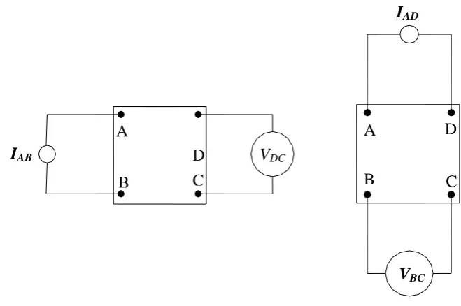
Fig. 2: A schematic diagram of four-point probe resistivity measurement
Electrical resistivity measurements of the thin films were done using the four point probe arrangement adopting the van der pauw method. With a symmetrical square geometry adopted, the probe leads were connected to the Keithly Source Meter for voltage and current measurements. The keithly SourceMeter operate by both sourcing and measuring at the same time. Four wire remote sensing was adopted since this minimizes errors due to potential drops in the test leads when sourcing or reading voltages and it ensured that the programmed voltage was delivered to the thin film under test. Figure 2 shows a schematic diagram of four-point probe resistivity measurement. A current of 1.0 x 10⁻¹⁰ A was applied through the contacts A and B and the potential drop across D and C measured. Sheet resistance of the samples was measured upon annealing at constant rate. This was done by placing the samples in a quartz tube of the electric furnace in argon ambient. The temperature was varied in the range between 25oC to 250oC. The measured values of current, voltage drops and film thickness were used to compute sheet resistivity.
3. Result and discussions
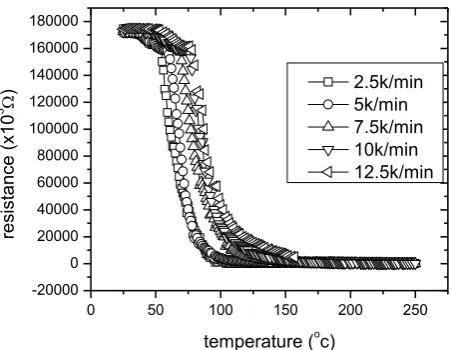
The thickness of the films was determined using Alpha-Step IQ surface profiler with a vertical resolution of 0.012Å and vertical range of 100 Å-0.4 mm. The profiler compares the thickness of a blank glass slide with that having a film. The film had a thickness of 185.0±0.05nm. Figure 3 shows the variation of sheet resistance vs. Temperature, upon annealing at a rate of 5K/min.
I
ABA
B
D
C
V
DCI
ADA
B
D
C
0 50 100 150 200 250 -20000
0 20000 40000 60000 80000 100000 120000 140000 160000
180000 5k/min
re
si
st
a
n
ce
(x1
0
3
)
temperature (oc)
Fig.3: Graph of temperature dependence of sheet resistance of In40Se60 films
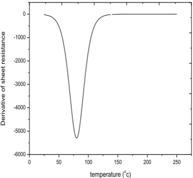
The as deposited sheet resistance was found to be 1.731 x 10⁸ Ω/Sq, after annealing this value reduced to 2.08 x 10² Ω/Sq. At the beginning of the measurement, the films had high resistance because they were in the amorphous phase. With increase in temperature, the resistance decreased. A one sharp drop in resistance indicated a phase transition from amorphous to crystalline. Crystallization temperature was obtained by differentiating the curve as shown in figure 4.
0 50 100 150 200 250 -6000
-5000 -4000 -3000 -2000 -1000 0
D
e
ri
va
ti
ve
o
f
sh
e
e
t
re
si
st
a
n
ce
temperature (o
c)
Fig.4: Derivative of sheet resistance vs. temperature for In40Se60
The transition temperature for In40Se60 was found to be 75.96±0.38oC. Although this value is lower than that obtained by Friedrich et al., 2000 for the widely used GST which is 149oC, it was much higher than room temperature. This is an important advantage for this alloy because it is essential to prevent self-transition of recording materials between the two phases; amorphous and crystalline. Hence one can expect the PRAM made from this alloy to remain stable in its amorphous and crystalline states at room temperature.
According to Chung et al., 2008, an electrical contrast of at least three orders of magnitude is required for a phase change material to be used for memory applications.
3.1 Activation energy of crystallization
In40Se60 thin films were annealed at heating rates of 2.5, 5, 7.5, 10 and 12.5k/min within the temperature range of 25oC to 250oC. Figure 5 shows the variation of sheet resistance versus temperature for samples annealed at different heating rates. There is a positive shift in transition temperature as the heating rates increase. The peak temperatures Tp at various heating rates were used to plot the Kissinger plots from where the activation energy of crystallization was determined. The value of the slope was used in the calculation of activation energy according to the following equation
ln(𝛽𝑇𝑃−2) = −∆𝐸
𝐾𝐵(
1
𝑇𝑃) + 𝑐𝑜𝑛𝑠𝑡𝑎𝑛𝑡
Where β is the heating rate, 𝑇𝑃 is peak crystallization temperature, ∆E is activation energy, 𝐾𝐵 is
Boltzmann constant. From the above equation, slope = - ∆𝐸𝐾
𝐵 and therefore the activation energy
∆E= slope x KB.
0 50 100 150 200 250
-20000 0 20000 40000 60000 80000 100000 120000 140000 160000 180000
re
si
st
a
n
ce
(x1
0
3
)
temperature (oc)
2.5k/min 5k/min 7.5k/min 10k/min 12.5k/min
Fig.5: Shift in transition temperature with change in heating rates.
2.3 2.4 2.5 2.6 2.7 -12.0
-11.5 -11.0 -10.5 -10.0 -9.5
ln
(
T
2)C
1000 T-1 C(K
-1
)
Fig.6: The Kissinger plots for calculation of activation energy for In40Se60 film
4. Conclusion
Crystallization kinetics of In40Se60 thin films has been successfully investigated. The crystallization temperatures were found to be much higher than room temperature and therefore a PRAM cell from this material will be stable at room temperature. High crystallization temperatures prevent self-transition of glassy alloys which is required for the application as stable glass. The film showed an electrical contrast of six orders of magnitude which is an advantage because an electrical contrast of at least three orders of magnitude is required for a phase change memory application. Activation energy of 0.538 ± 0.063eV was determined for In40Se60 alloy. This value is high implying high data stability for PCM devices employing In40Se60 alloy as the active layer.
References
[1] P Agarwal, S Goel, SK Tripathi, A Kumar, Physica B. 172, 511 (1991). [2] A Ates, M Kundakci, A Astam, M Yildrim, PhysicaE. 40, 2709 (2008).
[3] GW Burr, MJ Breitwisch, M Francheschini, D Garetto, K Goparakrishna, B Jackson, B Kurdi, C Lam, LA Lastras, A Padilla, B Rajidan, S Raoux, RS Shenoy, J. Vac. Sci. and Technol. 28, 223 (2010).
[4] Y Choi, M Jung, Y Lee, Electrochem. and Solid-state Lett. 12(7), F17 (2009). [5] KM Chung, D Wamwangi, Woda, M Wuttig, W Bensch, J. Appl. Phys. 10(8), 083523. (2008).
[6] I Friedrich, V Weidenhof, W Njoroge, P. Franz, M Wuttig J. Applied Physics 87, 4130 (2000).
[7] S Raoux Phase change materials. Ann. Rev. Mater. Res. 39, 25 (2009). [8] L Heone, K Dae-Hwan, Mater. Sci. and Eng. B119, 196 (2005).
[9] G Kaur, T. Komatsu,J. Mater. Sci. 36, 4531 (2000).
[10] N Mehta, M Zulfequar, A Kumar, Phys. Stat. Sol. 203, 236 (2005). [11] WK Njoroge, M Wuttig, J. Appl. Phys. 90(8), 3816 (2001).
[12] J Poortmans, V Arkhipov, Thin film solar cells fabrication, characterization and applications. John Wiley and Sons. Chinchester. (2006).
[13] S Raoux, J L Jordan-sweet, AJ Kelloc, J. Appl. Phys. 103(11), 114310 (2008).
[14] J Sharma Preparation and characterization of selenium based nanocrystalline thin films. PHD thesis, Punjab University, Chandigarh. (2007).
[15] R Shukla, P Agarwal, A Kumar, Chalcogenide letters. 7, 249 (2010).