ISSN (Print) : 2320 – 3765 ISSN (Online): 2278 – 8875
I
nternational
J
ournal of
A
dvanced
R
esearch in
E
lectrical,
E
lectronics and
I
nstrumentation
E
ngineering
(A High Impact Factor, Monthly, Peer Reviewed Journal)
Website: www.ijareeie.com
Vol. 7, Issue 5, May 2018
Reduction in DC Bus Capacitor with help of
Design control system
Nilesh R Thakre 1, Pankaj J Bhakre2, K.Chandra Obula Reddy 3
PG Student [EPS], Dept. of EE, MSS’s College of Engineering and Technology, Jalna, India 1 Professor, Dept. of EE, MSS’s College of Engineering and Technology, Jalna, India2 Professor, Dept. of EE, MSS’s College of Engineering and Technology, Jalna, India 3
ABSTRACT:AC and DC microgrids are often using single phase rectifier when power supplying to DC loads. Such rectifiers have high performance parameter like high reliability, high Power density, high efficiency with low costs. For volume-critical and weight-critical applications, such as electrical vehicles and aircraft power systems the volume and weight of bulky electrolytic capacitors could be a serious problem. This Paper investigated a single-phase four-switch rectifier with considerably reduced capacitance. Upper and Lower Capacitor split the DC bus into rectifier leg and neutral leg. The ripple energy in the rectifier is bypass through the lower split capacitor so that the voltage across the upper split capacitor produces the DC output voltage which has very small ripples. So that the total capacitance needed is significantly reduced and highly reliable film capacitors can be used instead of electrolytic capacitors.
KEYWORDS: Single Phase rectifier, Reliability, Power density, Electrolytic capacitor, Film capacitor.
I.INTRODUCTION
Conventionally, bulky electrolytic capacitors are required for single-phase rectifiers to produce smooth DC-bus voltage, due to the pulsating input power. Main problem of electrolytic capacitors is to have limited lifetime, are one of the most vulnerable components in power electronic systems. So in order to enhance the reliability of power electronic systems, it is highly desirable to minimize the usage of electrolytic capacitors and use highly-reliable small capacitors like film capacitors while maintaining low voltage ripples.
K. Yao, X. Ruan, X. Mao, and Z. Ye ,[1] is deals with reduction of the DC-bus capacitor by injecting third harmonics component to the grid current. R. Wang, F. Wang, D. Boroyevich, R. Burgos, R. Lai, P. Ning, and K. Rajashekara, [2] was discuss reduction in DC-bus capacitor by adding an active energy storage compensator in parallel with DC-bus capacitors in order to bypass ripple energy that basically flowing through the DC-bus capacitors. Basically the added compensator is operated as buck/boost converters to inject/absorb ripple currents from DC-bus. H. Wang, H.-H.Chung, and W. Liu,[3] is deals with such proposed system in which an active compensator connecting in series with the DC bus. It behaves as a voltage source to offset voltage ripples. P. Krein, R. Balog, and M. Mirjafari ,[4] is deals with a system which introduced a ripple port terminated with capacitor to store the ripple power. W.-L. Ming and Q.-C.Zhong [5] deals with a 4-switch rectifier which was proposed to significantly reduce the DC-bus capacitance in the widely-adopted asymmetrical single-phase systems, where the midpoint of the AC side is not available. This paper presents the further work of W.-L. Ming and Q.-C.Zhong ,[5] where we can control the output voltage V+, reducing the value of capacitor and maintaining the almost unity power factor simultaneously.
ISSN (Print) : 2320 – 3765 ISSN (Online): 2278 – 8875
I
nternational
J
ournal of
A
dvanced
R
esearch in
E
lectrical,
E
lectronics and
I
nstrumentation
E
ngineering
(A High Impact Factor, Monthly, Peer Reviewed Journal)
Website: www.ijareeie.com
Vol. 7, Issue 5, May 2018
II. SINGLE PHASE RECTIFIER
The rectifier can be formed by adding two active switches into a conventional half-bridge PWM rectifier by putting a neutral leg consisting of two switches across the DC bus with their midpoint connected to the midpoint of the split capacitors through an inductor. In particular, the neutral leg has been applied to three phase Where V+ and V− are the voltages across the split capacitors C+ and C− with respect to the neutral point N.
t
V
v
t
I
i
g g
g g
sin
sin
Figure: 2.1 single-phase rectifier under investigation.
Because the switches are operated at a frequency much higher than the fundamental frequency, the averaged variables, e.g. average currents and average voltages, can be adopted to well represent the original variables according to the averaging theory the circuit can be analysed by using the average circuit model as per R. Srinivasan and R. Oruganti ,[6]. According to the average circuit model of the rectifier shown in Figure 2.2, the capacitor currents can be found as
(1)
four-wire power inverters as reported in [7]. By diverting all the ripple power to the lower capacitor C−, the output voltage V+ can become ripple free, which means the output capacitance C+ can be reduced a lot because it does not need to process any low frequency ripple energy. Importantly, the capacitor C− can also be significantly reduced because its voltage is not supplied to any loads so it can be designed to have large ripples on purpose.
)
1
(
)
1
(
3 2
3 2
d
i
d
i
i
d
i
I
d
i
i
L g C
L R g
C
ISSN (Print) : 2320 – 3765 ISSN (Online): 2278 – 8875
I
nternational
J
ournal of
A
dvanced
R
esearch in
E
lectrical,
E
lectronics and
I
nstrumentation
E
ngineering
(A High Impact Factor, Monthly, Peer Reviewed Journal)
Website: www.ijareeie.com
Vol. 7, Issue 5, May 2018
Figure: 2.2 The average circuit model of the rectifier shown in Figure 2.1.
It is assumed that the DC-bus voltage of the rectifier
(2) And neutral current can be found as
(3)
Since the switching frequency is much higher than the line frequency, the duty cycle of Switch Q2 can be calculated in the average sense as
(4)
The duty cycle of Switch Q3 can be calculated as
(5)
And the load current is
(6)
If the neutral current is controlled to provide the DC component only, that is,
(7) Then the capacitor currents are,
(8) and
(9)
III. REDUCTION OF CAPACITANCE
The idea is to push the current components of
i
c through the neutral leg instead of through the upper split capacitor so thati
c does not contain any fundamental or second order ripple currents. That is to makei
c = 0, ignoring the switching ripples. the currenti
L should be controlled to satisfy(10)
V
V
V
DCR g C C
L
i
i
i
I
i
V
I
V
t
V
I
V
i
i
L g g g g g2
2
cos
2
t
V
I
V
i
V
V
i
DC g g g DCC
cos
2
2
t
V
I
V
i
V
V
i
DC g g g DCC
cos
2
2
R LI
i
V
I
V
I
R g g2
DC
V
V
d
3
_t
V
V
V
V
d
DC g DC
sin
2
ISSN (Print) : 2320 – 3765 ISSN (Online): 2278 – 8875
I
nternational
J
ournal of
A
dvanced
R
esearch in
E
lectrical,
E
lectronics and
I
nstrumentation
E
ngineering
(A High Impact Factor, Monthly, Peer Reviewed Journal)
Website: www.ijareeie.com
Vol. 7, Issue 5, May 2018
On the other hand,
i
L should also satisfy. Hence, in this case, the current flowing through the lower split capacitor should be(11)
In other words, it only contains the second-order harmonic component or the second-order component only flows through the lower split capacitor. As a result, all the voltage ripples are then diverted to the lower capacitor C− , which would increase the voltage ripples on C− . However, this does not matter because there is no load connected to V− and the voltage V− can tolerates a much higher ripple voltage. Hence, only a small C− is needed. Since the upper capacitor C+ does not contain any fundamental and second-order ripple voltage components any more, it can be reduced a lot while maintaining low voltage ripples. As a result, both capacitors C+ and C− can be very small, which makes it possible to replace the required bulky electrolytic capacitors with film capacitors.
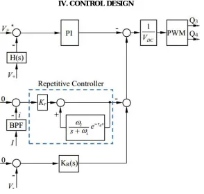
IV. CONTROL DESIGN
Figure 4.1 Control System for controlling Neutral leg.
The neutral leg should be controlled to maintain the output voltage V+, to remove the ripple components in iC+ and also to remove the fundamental component in iC−.Maintaining a stable output voltage V+ with very small ripples at the desired output reference voltage V *+ is a major target. The neutral leg is responsible for splitting the DC-bus voltage into V+ and V−, which are independent from each other. Since the voltage V+ is used as the output voltage. it can be directly controlled by forming a voltage loop and then the voltage V− can be indirectly controlled by regulating the DC-bus voltage. In order to regulate the output voltage V+, it is measured and put through the hold filter.
(12)
Ts
e
s
H
Ts
1
)
(
t
V
I
V
i
C g gcos
2
2
ISSN (Print) : 2320 – 3765 ISSN (Online): 2278 – 8875
I
nternational
J
ournal of
A
dvanced
R
esearch in
E
lectrical,
E
lectronics and
I
nstrumentation
E
ngineering
(A High Impact Factor, Monthly, Peer Reviewed Journal)
Website: www.ijareeie.com
Vol. 7, Issue 5, May 2018
A simple proportional-integral (PI) controller is then applied to regulate the voltage. The output of the PI controller can be converted to PWM signals to drive the switches. The parameters for the PI controller can be selected according to classical design methods for a second-order system, with the characteristic equation given by
(13)
where Kp and Ki are the gains of the PI controller. These parameters can be chosen to obtain the damping coefficient of (14)
Removal of fundamental component in iC−: The control of the DC-bus ripple current i to 0 leads to the fact that the ripples are now diverted to the lower capacitor C−. In this case, the current of the capacitor C− is expected to only have a second-order component. When i = 0, there is ig = iL − iC− + IR, which means that the grid current ig could flow through the inductor LN and the capacitor
C− if not controlled properly. Hence, there is a need to make sure that no fundamental component flows through the capacitor C−
otherwise it would lead to increased voltage ripples without providing any benefits. This can be achieved by forcing the fundamental component of V− to be zero, The following resonant
(15)
The output of the resonant controller is then added onto the outputs of the other two controllers before sending to the PWM conversion block, as shown in Figure 3. The gain Kh of the resonant controller can be selected by fine tuning through trial-and-error in practice; it is chosen as Kh = 10 for the experimental system to be tested. In general, a large gain should improve the performance of the control but may lead to a large charging current when starting up the system that might trigger the current protection and also may introduce noticeable disturbance into the current controller. These should be avoided. Note that the output of this controller is “+” because the voltage under control relates to V−.
Figure 4.2 Control System for controlling Rectification leg.
2 2
)
(
2
2
)
(
h
s
h
s
s
h
K
s
K
hR
2
1
1
2
i
P
K
C
K
0
2
C
K
s
C
K
ISSN (Print) : 2320 – 3765 ISSN (Online): 2278 – 8875
I
nternational
J
ournal of
A
dvanced
R
esearch in
E
lectrical,
E
lectronics and
I
nstrumentation
E
ngineering
(A High Impact Factor, Monthly, Peer Reviewed Journal)
Website: www.ijareeie.com
Vol. 7, Issue 5, May 2018
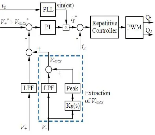
Main purpose to control the Rectification Leg is to control the grid current and control the DC bus voltage. Grid current should be in phase with Grid voltage and free from harmonics. By using PLL generating reference Current i* and Dc bus voltage is keep constant at V+* +V*_max . In order to extract the second-order component, the resonant filter with
= 0.01, h = 2, and
= 2πf.For the rectification leg, there are two switches and two diodes in total. The current flowing through the rectification leg mainly depends on the grid current ig. The positive cycle of the grid current ig flows through the Switch Q2 and the corresponding free-wheeling diode is D1. On the other hand, the negative cycle of the grid current ig flows through the Switch Q1 and the the corresponding free-wheeling diode is D2.
)
5
.
0
2
(
)
1
(
2
1
2 21
g R g QV
V
I
dt
d
i
I
)
5
.
0
2
(
2
1
0 22
g R g QV
V
I
dt
d
i
I
)
5
.
0
2
(
)
1
(
2
1
0 21
g R g DV
V
I
dt
d
i
I
)
5
.
0
2
(
2
1
2 0 22
g R g DV
V
I
dt
d
i
I
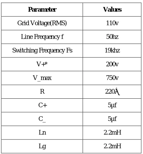
V. DESIGN EXAMPLE
Table 1 System Parameter
Parameter Values
Grid Voltage(RMS) 110v
Line Frequency f 50hz
Switching Frequency Fs 19khz
V+* 200v
V_max 750v
R 220Ω
C+ 5µf
C_ 5µf
Ln 2.2mH
ISSN (Print) : 2320 – 3765 ISSN (Online): 2278 – 8875
I
nternational
J
ournal of
A
dvanced
R
esearch in
E
lectrical,
E
lectronics and
I
nstrumentation
E
ngineering
(A High Impact Factor, Monthly, Peer Reviewed Journal)
Website: www.ijareeie.com
Vol. 7, Issue 5, May 2018
Let , allowable maximum Peak to Peak ripple current which flow through the inductor
i
LM= 4A , Then Minimum inductance is calculated as(16)
min
N
L
= 2.1mH , 2.2mH selected hereThe capacitor C− can be selected based on C−min and
i
Cmax express as followWhere
i
Cmax = the maximum second-order ripple current(17)
max
C
i
= 1A(18)
Here Ig=3A used
min
C
=2.69 uF ; to leave some margin the C- selected as C- = 5uFFor the selection of the capacitor C+
(19)
min
C
≈5 μF.For the selection of the capacitor
C
min, if the maximum switching ripple voltageV
sm is expected to be around 5 V, thenC
min ≈5 μF.If we are using traditional Single phase rectifier then DC capacitor should be larger than ,
(20)
If we compare the result of (19) and (20) then understand that This means the DC-bus capacitors can be reduced by over 70 times while maintaining the same level of output voltage ripples.
F
V
V
I
V
ave g g
386
.
8
2
sm s LM
V
f
i
C
8
min)
(
max max min
V
V
f
i
V
V
L
s LM N2
/
max max g g g ave g g CV
V
I
V
V
I
V
i
)
(
2max 2 max 3 min MinV
V
I
V
f
L
d
V
C
g gs
N
ISSN (Print) : 2320 – 3765 ISSN (Online): 2278 – 8875
I
nternational
J
ournal of
A
dvanced
R
esearch in
E
lectrical,
E
lectronics and
I
nstrumentation
E
ngineering
(A High Impact Factor, Monthly, Peer Reviewed Journal)
Website: www.ijareeie.com
Vol. 7, Issue 5, May 2018
in order to maintained the output ripple voltage around 5V the electrolytic capacitors are often needed. The experimental results presented later show that the rectifier under investigation can achieve 5 V output ripple voltage only with two 5 μF film capacitors.
VI. EXPERIMENTAL RESULT
Result Analysis Shows waveform of the grid current ig and the DC voltages V+ and V− the system steady-state performance with V ∗+ = 200 V is given in Figure 6(1)-(8) for V ∗−max = 600, V ∗−max = 650, V ∗−max = 700 and V
−
∗ max = 750, respectively. It is clear that the DC output voltage V+ is always maintained around its reference 200 V while the ripple voltage of V− varies from 329 V to 430V depending on the maximum voltages of V−. Importantly, the voltage ripples of the voltage V+ are only about 5 V when V ∗−max = 700 V and 750 V. As a result, nearly all the ripple power is now stored on the lower capacitor C− instead of both C+ and C− over a wide range of V−.
Figure 6.1
The grid current ig , grid voltage
v
g and the DC voltages V+ and V- withV
200
V
*
,
V
600
V
* max
is given
in Figure 6.1. It is clear that the DC output voltage V+ is always maintained around its reference 200 V while the ripple voltage of V− is 430V.
ISSN (Print) : 2320 – 3765 ISSN (Online): 2278 – 8875
I
nternational
J
ournal of
A
dvanced
R
esearch in
E
lectrical,
E
lectronics and
I
nstrumentation
E
ngineering
(A High Impact Factor, Monthly, Peer Reviewed Journal)
Website: www.ijareeie.com
Vol. 7, Issue 5, May 2018
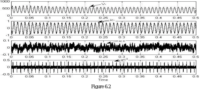
The waveforms of the DC-bus current I and the capacitors currents
i
C andi
C withV
*
200
V
whenV
V
max*
600
is given in Figure 6.2. It is clear that AC component of the DC-bus current and the currenti
C arealways maintained around zero for voltage
V
max*
600
V
. The ripples of the capacitor currenti
C are relatively large because all the ripple power is now stored on the capacitor C−.Figure 6.3
The grid current ig , grid voltage
v
g and the DC voltages V+ and V- withV
*
200
V
V
650
V
* max
is given
in Figure 6.3. It is clear that the DC output voltage V+ is always maintained around its reference 200 V while the ripple voltage of V− is 410V.
ISSN (Print) : 2320 – 3765 ISSN (Online): 2278 – 8875
I
nternational
J
ournal of
A
dvanced
R
esearch in
E
lectrical,
E
lectronics and
I
nstrumentation
E
ngineering
(A High Impact Factor, Monthly, Peer Reviewed Journal)
Website: www.ijareeie.com
Vol. 7, Issue 5, May 2018
The waveforms of the DC-bus current I and the capacitors currents
i
C andi
C withV
*
200
V
whenV
V
max*
650
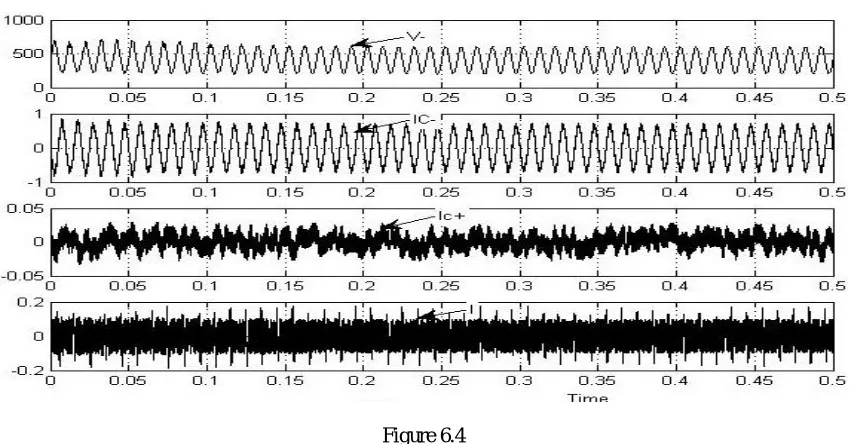
is given in Figure 6.4. It is clear that AC component of the DC-bus current and the currenti
C arealways maintained around zero for Voltage
V
max*
650
V
. The ripples of the capacitor currenti
C are relatively large because all the ripple power is now stored on the capacitor C−.Figure 6.5
The grid current ig , grid voltage
v
g and the DC voltages V+ and V- withV
200
V
*
V
700
V
* max
is given
in Figure 6.5. It is clear that the DC output voltage V+ is always maintained around its reference 200 V while the ripple voltage of V− is 345V.
ISSN (Print) : 2320 – 3765 ISSN (Online): 2278 – 8875
I
nternational
J
ournal of
A
dvanced
R
esearch in
E
lectrical,
E
lectronics and
I
nstrumentation
E
ngineering
(A High Impact Factor, Monthly, Peer Reviewed Journal)
Website: www.ijareeie.com
Vol. 7, Issue 5, May 2018
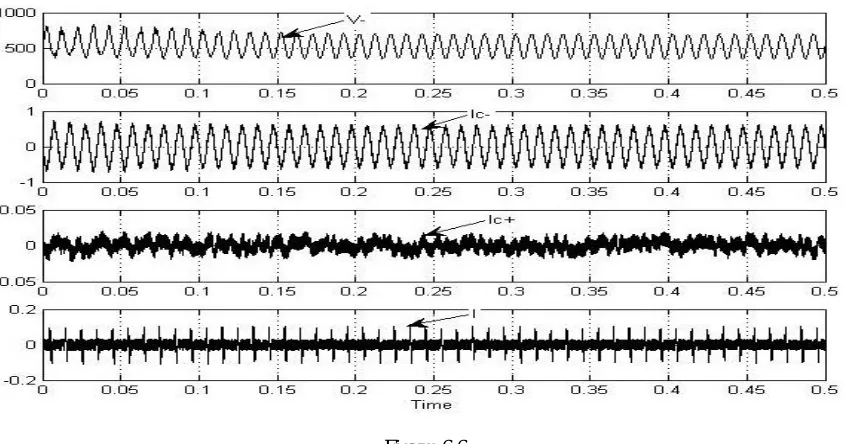
The waveforms of the DC-bus current I and the capacitors currents
i
C andi
C withV
*
200
V
whenV
V
max*
700
is given in Figure 6.6. It is clear that AC component of the DC-bus current and the currenti
C arealways maintained around zero for voltage
V
max*
700
V
. The ripples of the capacitor currenti
C are relatively large because all the ripple power is now stored on the capacitor C−.Figure 6.7
The grid current ig , grid voltage
v
g and the DC voltages V+ and V- withV
200
V
*
V
750
V
* max
is given
in Figure 6.7. It is clear that the DC output voltage V+ is always maintained around its reference 200 V while the ripple voltage of V− is 329V.
ISSN (Print) : 2320 – 3765 ISSN (Online): 2278 – 8875
I
nternational
J
ournal of
A
dvanced
R
esearch in
E
lectrical,
E
lectronics and
I
nstrumentation
E
ngineering
(A High Impact Factor, Monthly, Peer Reviewed Journal)
Website: www.ijareeie.com
Vol. 7, Issue 5, May 2018
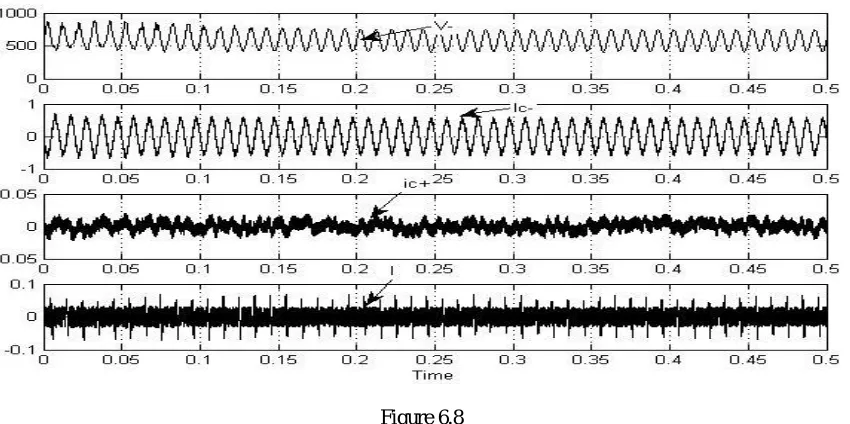
The waveforms of the DC-bus current I and the capacitors currents
i
C andi
C withV
*
200
V
whenV
V
max*
750
is given in Figure 6.8. It is clear that AC component of the DC-bus current and the currenti
C arealways maintained around zero for voltage
V
max*
750
V
. The ripples of the capacitor currenti
C are relatively large because all the ripple power is now stored on the capacitor C−.It indicates that Dc output Voltage V+ is maintained around 200v while the ripple voltage of V- varies from 329v to 430v which depends on maximum voltages of V-.Grid current ig is always in phase with the grid voltage so unity power factor is achieved. As per recorded results THD of the grid current is around 4% and input Power factor is above the 0.99 for all cases
VII. CONCLUSION
In this proposed system we are able to reduce the value of capacitor by 70 times if we compare it with traditional single phase rectifier. Both the capacitor can be reduced to a level where film capacitors are to be selected which is much precise, light weight and cost effective. Result indicates that rectification Leg of rectifier is effectively used to maintain the grid current and DC bus voltage. Grid current ig is always in phase with the grid voltage so unity power factor is achieved. As per recorded results THD of the grid current is around 4% and input Power factor is above the 0.99 for all cases.
REFERENCES
[1] K. Yao, X. Ruan, X. Mao, and Z. Ye, “Reducing storage capacitor of a DCM Boost PFC converter,” IEEE Trans. Power Electron., vol. 27, no. 1 pp. 151–160, Jan. 2012.
[2] R. Wang, F. Wang, D. Boroyevich, R. Burgos, R. Lai, P. Ning, and K. Rajashekara, “A high power density single-phase PWM rectifier with active ripple energy storage,” IEEE Trans.Power Electron., vol. 26, no. 5, pp. 1430–1443, May 2011.
[3] H. Wang, H.-H.Chung, and W. Liu, “Use of a series voltage compensator for reduction of the
DC-link capacitance in a capacitorsupported system,” IEEE Trans. Power Electron., vol. 29, no. 3, pp. 1163–1175, 2014.
[4] P. Krein, R. Balog, and M. Mirjafari, “Minimum energy and capacitance requirements for single-phase inverters and rectifiers using a ripple port,”IEEE Trans. Power Electron., vol. 27, no. 11, pp. 4690–4698, Nov. 2012.
[5] W.-L. Ming and Q.-C.Zhong, “Single-phase half-bridge rectifiers with extended voltage range and reduced voltage ripples,” in Power Electronics for Distributed Generation Systems (PEDG), 2014 IEEE 5thInternational Symposium on, 2014, pp. 1–6.
[6] R. Srinivasan and R. Oruganti, “A unity power factor converter using half-bridge boost topology,” IEEE Trans. Power Electron., vol. 13, no. 3, pp. 487–500, 1998.
[7] N. Mohan, Power electronics: converters, applications, and design. Hoboken, NJ : John Wiley and Sons, 2003.
[8] H. Fujita, “A high-efficiency solar power conditioner using a zigzagconnected chopper converter,” in Power Electronics Conference (IPEC), 2010 International, 2010, pp. 1681–1687.
[9] D. Karschny, “Wechselrichter,” German Patent DE19 642 522 C1, Apr., 1998.
[10] T. Hornik and Q.-C. Zhong, “A current control strategy for voltagesource inverters in microgrids based on H1 and repetitive control,” IEEE Trans. Power Electron., vol. 26, no. 3, pp. 943–952, Mar. 2011.
[11] X. Cao, Q. Zhong, and W. Ming, “Ripple eliminator to smooth DCbus voltage and reduce the total capacitance required,” IEEE Trans. Ind. Electron., to be published, early Access.