ISSN 2348 – 7968
Implementation of an Efficient Multiplier based on Vedic Mathematics
Using High speed adder
Ankit Chouhan1, Mr. Arvind Pratap Singh2 1
Department of Electronics and Communication, Medicaps Institute of Technology & Management, Indore, Madhya Pradesh, India
2
Department of Electronics and Communication, Medicaps Institute of Technology & Management, Indore, Madhya Pradesh, India
Abstract
A high speed controller or processor depends vastly on the multiplier as it is one of the main hardware blocks in most digital signal processing unit as well as in general processors. This paper presents a high speed Vedic multiplier architecture which is quite different from the Conventional Vedic multiplier. The most significant aspect of the proposed method is that, the developed multiplier architecture uses Carry look ahead adder as a key block for fast addition. Using Carry look ahead adder the performance of multiplier is vastly improved. This also gives chances to break whole design into smaller blocks and use it whenever required. So by using structural modeling we can easily make large design by using small design and thus complexity gets reduced for inputs of larger no of bits. We had written code for proposed new Vedic multiplier using VHDL (Very High Speed Integrated Circuits Hardware Description Language), synthesized and simulated using XilinxISE8.1i and downloaded to Spartan2 FPGA device. Finally the results are compared with Conventional Vedic multipliers to show the significant improvement in its combinational path delay (speed). The high speed processor requires high speed multipliers and the new Vedic Multiplication technique is very much suitable for this purpose.
Keywords: Architecture, Carry look ahead (CLA) Adder, Multiplication, Vedic Mathematics, Vedic Multiplier (VM), Urdhava Tiryakbhyam Sutra,VHDL.
1. Introduction
In most of the digital signal processing applications the main operation is multiplication and the speed of the digital signal processors is mainly determined by the speed of the multipliers used in the processor. The execution time of most digital signal processors algorithms depends on it multipliers and hence need for high speed multiplier arises , so to reduce the delay and speed up the digital signal processors a new multipliers are designed using Vedic mathematics techniques.
Vedic mathematics is mainly based on 16 sutras (or aphorisms) and was re discovered in twentieth century. The proposed multiplier technique is from” urdhva
tiryakbhayam sutra “which is one of the sutras in Vedic mathematics. Now we are going to code this technique in VHDL and synthesis using XilinxISE8.1i. So we can calculate delay, speed, and execution time of the proposed multiplier and can see the performance of multiplier by comparing to some standard multipliers.
2. Vedic Multiplication Technique
2.1 Urdhva Tiryakbhyam Sutra
ISSN 2348 – 7968
slowly when compared with other basic multipliers, which is the main advantage of the multiplier. Therefore, it is time, area and power efficient. Hence, this architecture is capable in terms of area/speed of silicon [1].
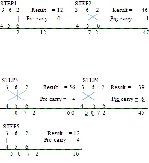
2.2 Multiplication of two decimal numbers 362 x 456
3. The Conventional Vedic Multiplier
Architecture
The designing of Vedic Multiplier is different from conventional multiplier like array multipliers. Even though both multiplier have the same number of multiplications, the array multiplier use some small blocks like shift and add for designing higher order multipliers. Vedic Multiplier is designed in VHDL, as it is more effective in structural way of coding. The individual block is implemented using VHDL language. The performance of each multiplier is determined using the xilinxISE8.1i. [2].
3.1 Vedic Multiplier for 2x2 bit Module
The One bit multipliers and adders are the basic building blocks the 2×2 multiplier. The two input AND gate is used to perform one bit multiplier and for one bit adder we can use full adder. The basic 2 × 2 bit multiplier block representation is shown in Fig. 1. [3].
Let us consider two data inputs, each of length 2 bits; say A1A0 and B1B0. The output can be of four bit length, say P3P2P1P0. As per basic method of multiplication, we can obtain the result by getting partial product and then by adding it. In Vedic multiplier, P0 is obtained by vertical multiplication of data bits A0 and B0, P1 is obtained by addition of crosswise bit product i.e.A1B0 and 𝐴𝐴0B1 and next P2 is obtained by adding the product vertical data bits A1 and B1 with the carry generated from the previous addition during P1. P3 is the nothing but carry generated in calculation of P2. This part is the operation of 2x2 multiplier block.
A1 A0 A1 A0 A1 A0
| |
B1 B0 B1 B0 B1 B0
Fig. 1 The Vedic Multiplication Method for two 2-bit Binary Numbers
3.2 Vedic Multiplier for 4x4 bit Module
As number of bits increases in input, a small modification is required. Divide the total number of bits of each input into two equal parts .Now let us implement 4x4 multiplications with inputs as A3A2A1A0 and B3B2B1B0. The result obtained by multiplication the two inputs are represented as P7P6P5P4P3P2P1P0.
Let us divide the inputs A and B into two equal parts as we mentioned above, say A3A2 and A1A0 for input A and B3B2 and B1B0 for input B. Take two bits at a time by using the basic principle of Vedic multiplication and using 2 bit Vedic multiplier block. [4].
ISSN 2348 – 7968
specific way. So we require three ripple carry adders at final stage as shown in Fig. 6.4. By observing the algorithm we can say that 4x 4 bit multipliers are designed from 2X2 bit blocks
A3 A2 A1 A0
B3 B2 B1 B0
Fig. 2 Sample Presentation for 4x4 bit Vedic Multiplication
3.3 Conventional Vedic Multiplier for 8x8 bit
Module
Fig. 3.Block Diagram of 8x8 bit Conventional Vedic Multiplier
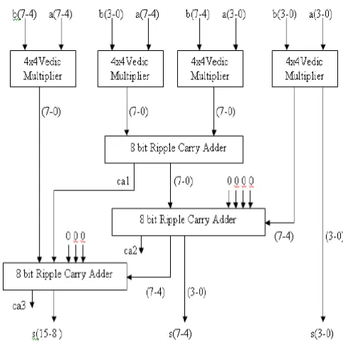
3.4 Proposed Vedic Multiplier for 8x8 bit Module
with carry lookahead adder.
Fig. 4 Block Diagram of 8x8 bit Proposed new Vedic Multiplier
We have designed 8x8 bit Vedic multiplier by using 4×4 multiplier and it is shown in the block in Fig. 4 that can be implemented by using four 4x4 bit Vedic multiplier blocks as discussed above. Let us implement 8x8 multiplications with inputs as A = A7A6A5A4A3A2A1A0 and B =
𝐵𝐵7B6B5B4B3B2B1B0. The result obtained by
multiplication of two 8-bit inputs is represented as P15P14P13P12P11P10P9P8P7P6P5P4P3P2P1P0. 8x8 Vedic Multiplier block diagram is shown in Fig 4. Now divide the inputs A and B into two equal parts, the 8 bit multiplicand A can be split into pair of four bits 𝐴𝐴H − 𝐴𝐴L. In Similarly way multiplicand B can be split into𝐵𝐵H− 𝐵𝐵L. The 16 bit result can be written as[5].
𝑃𝑃 = 𝐴𝐴 × 𝐵𝐵
= (𝐴𝐴H − 𝐴𝐴L) × (𝐵𝐵H−𝐵𝐵L)
=(𝐴𝐴H × 𝐵𝐵L) + (𝐴𝐴H × 𝐵𝐵L) + ( 𝐴𝐴H × 𝐵𝐵L) + (𝐴𝐴H × 𝐵𝐵L) Where
𝐴𝐴H = 𝐴𝐴7𝐴𝐴6𝐴𝐴5𝐴𝐴4 𝐴𝐴L = 𝐴𝐴3𝐴𝐴2𝐴𝐴1𝐴𝐴0 𝐵𝐵H = 𝐵𝐵7𝐵𝐵6𝐵𝐵5𝐵𝐵4
ISSN 2348 – 7968
By observing the structural implementation block diagram of 8×8 Vedic multiplier as shown in Fig. 4, we require four 4×4 multipliers and ripple carry lookahead adders. The outputs of four 4×4 bit multipliers are added according with three 8-bit CLA as in Fig 4, in order to obtain the final product. Thus, 4×4 Vedic multipliers are the basic building blocks to implement 8×8 Vedic multiplier. In similar way we can implement higher bit multiplier such as 16, 32, and 64.
3.5 Why carry Carry lookahead adder?
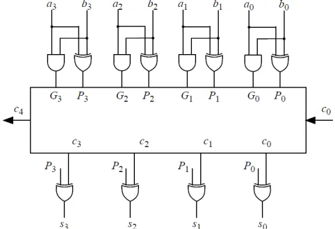
In a ripple carry adder an adder cell uses the carry output from its previous cell to generate its sum and its carry output. This is unlike a carry-lookahead adder that generates its carry bits based on the bits of the data inputs, instead of relying on carry bits from the previous bits. A carry-lookahead adder is faster than a ripple-carry adder because independence of a carry bit on its previous bits eliminates the otherwise carry generation gate delays .On the other hand, a carry-lookahead adder requires more hardware for generating carry signals of each other cell independent of the previous carry outputs. The following shows the hardware of a carry-lookahead adder and illustrates how it works. In what follows ai and bi are data input of bit I of an adder cell, and Ci is its carry input. Ci+1 is the carry output and Si is the sum. The term Pi is propagate since if it is ‘1’ it causes Ci to propagate to Ci+1.The gi term is called generate, because it generates Ci+1 if it is ‘1’.Using Pi,Gi,ai,bi and Co,C4 of a 4-bit carry lookahead adder is calculated as shown below.[6]
Ci+1 = ai bi + (ai XOR bi) Ci (3)
Si = (ai XOR bi) XOR Ci (4)
The above two equations can be written in terms of two new signals and, which are shown in Figure 5:
Fig. 5 Full adder at stage I with Pi and Gi shown
Ci+1 = Gi + PiCi (5)
Si = Pi XOR Ci (6)
Where
Gi=ai *bi (7)
Pi = ai XOR bi (8)
Let’s apply this to a 4-bit adder to make it clear.
Putting i = 0,1,2,3 in equation 5, we get
C1 = G0 +P0C0. (9)
C2 = G1 + P1G0 + P1P0C0. (10)
C3 = G2 + P2G1 + P2P1G0 + P2P1P0C0. (11)
C4 = G3 + P3G3 + P3P2G1 + P3P2P1G0 +P3P2P1P0C0. (12)
Figure 6 show that a 4-bit Carry lookahead adder is built using gates to generate the Pi and Gi signals and a logic block to generate the carry out signals according to Equations 9–12.
Fig. 6.Block Diagram 4-Bit carry lookahead adder implementation detail.
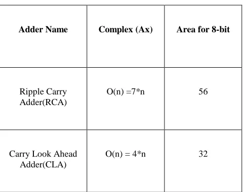
3.6 Theoretical Comparison of Carry look ahead
adder with Ripple carry adder for n =8
ISSN 2348 – 7968
Adder Name Complex (Ax) Area for 8-bit
Ripple Carry Adder(RCA)
O(n) =7*n 56
Carry Look Ahead Adder(CLA)
O(n) = 4*n 32
Table 2: Theoretical Comparison of Time Required (T)
Adder Name Complex (T) Delay for n-bit
Ripple Carry Adder(RCA) O(n) = 2*n 16
Carry Look Ahead Adder(CLA)
O(n) = 4 *log2(n) 12
Table 3: Theoretical Area Delay Product (Axt)
Adder Name Complex (T) Delay for n-bit
Ripple Carry Adder(RCA) O(n) = 2*n 16
Carry Look Ahead O(n) = 4 *log2(n) 12
Adder(CLA)
4. Implementation In Xilinx 8.1i
In this work, 8x8 bit Vedic multiplier is designed in VHDL (Very High Speed Integrated Circuits Hardware Description Language). Logic synthesis and simulation was done using tool in XilinxISE8.1i - Project Navigator and ISim simulator integrated in the Xilinx package. The performance of circuit is evaluated on the Xilinx device family Spartan3, package pq208 and speed grade -5.
Later the design is downloaded on Spartan2 due to unavailability of Spartan3 FPGA device.
Our proposed Vedic multiplier gives significant improvement over conventional vedic multiplier as we increase number of input bits of the multiplier.
So to check this first we have write code for conventional Vedic multiplier and then compare with our proposed Vedic multiplier and result is shown below in synthesis results
Fig. 7 RTL schematic of 8x8 bit new Vedic Multiplier
Fig. 8 Simulation Result of 8x8 bit new Vedic Multiplier.
ISSN 2348 – 7968
Fig. 9 Live picture of working on Spartan2
5. Result and Discussion
5.1 Device utilization summary:
Selected Device : 3s50pq208-5
Number of Slices: 94 out of 768 12% Number of 4 input LUTs: 164 out of 1536 10% Number of bonded IOBs: 32 out of 124 25%
5.2 Synthesis result:
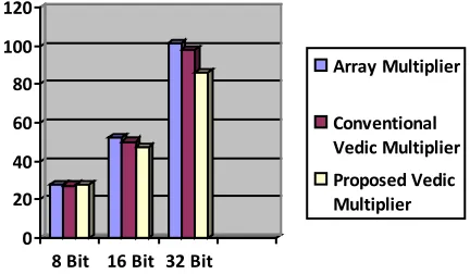
Table 4: Comparison Of Different Multipliers (In Ns)
Device: Spartan xc3s50a-5-pq144
Array Multiplier
Vedic Multiplier
New proposed Vedic Multiplier
Path Delay For n =8bit
27.796ns 27.463ns 27.903ns
Path Delay For n =16bit
52.708ns 50.299ns 47.613ns
Path Delay For n=32bit
101.486ns 98.067ns 86.495ns
Table IV shows the comparison of 8x8,16x16,32x32 bit Conventional multipliers with our new proposed Vedic multiplier (ours) in terms of computational path delay in nanoseconds (ns). The path delay for Array and conventional Vedic multipliers have been calculated by us only. The timing result shows that new Vedic multiplier has the greatest advantage as compared to other multipliers in terms of execution time.
6. Conclusion
This paper presents a highly efficient method of multiplication – “Urdhva Tiryakbhyam Sutra” based on Vedic mathematics. It gives us method for modular multiplier design and clearly indicates the computational advantages offered by Vedic methods. The computational path delay for proposed new Vedic multiplier is found to be less as compared to other multiplier. Hence our motivation to reduce delay is finely fulfilled. Therefore, we observed that the new Vedic multiplier is much more efficient than Array and conventional multiplier in terms of execution time (speed). An awareness of Vedic mathematics can be effectively increased if it is included in engineering education. In future, all the major universities may set up appropriate research centers to promote research works in Vedic mathematics.
0 20 40 60 80 100 120
8 Bit 16 Bit 32 Bit
Array Multiplier
ISSN 2348 – 7968
References
[1] Jagadguru Swami, Sri Bharati Krisna, Tirthaji Maharaja, “Vedic Mathematics or Sixteen Simple Mathematical Formulae from the Veda, Delhi (1965)”, Motilal Banarsidas, Varanasi, India, 1986.
[2] Pushpalata Verma, K. K. Mehta “Implementation of an Efficient Multiplier based on Vedic Mathematics Using EDA Tool,” International Journal of Engineering and Advanced Technology (IJEAT)
[3] B. Vamsi krishna & k. Dhanunjaya, “analysis and modeling of low power array multipliers usingcadence virtuoso simulator in 45 nm technology” International Journal of Electronics, Communication &Instrumentation Engineering Research andDevelopment (IJECIERD)ISSN 2249-684XVol. 3, Issue 4, Oct 2013, 49-64© TJPRC Pvt. Ltd.
[4] Pushpalata Verma,” Design of 4x4 bit Vedic Multiplier using EDA Tool”, nternational Journal of Computer Applications (0975–888) Volume 48 –No.20, June 2012.
[5] M.Sabarinathan,G,Omprakash,S.Ramachandra
&V.Balamurugan,”A high speed and less areamultiplier forhigh speedprocessor by SDT technique.International Journal of Electronics and Communication Engineering (IJECE) ISSN 2278-9901 Vol. 2, Issue 2, May 2013, 3342 © IASETK.