(Thesis format: Monograph)
by
Shawon Senjuti
Graduate Program in Electrical and Computer Engineering
A thesis submitted in partial fulfillment
of the requirements for the degree of
Master of Engineering Science
The School of Graduate and Postdoctoral Studies
The University of Western Ontario
London, Ontario, Canada
c
Wireless power transmission is a technique that converts energy from radio frequency (RF) electromagnetic (EM) waves into DC voltage, which has been used here for the purpose of providing a power supply to bio–implantable batteryless sensors. The main constraints of the design are to achieve the minimum power required by the application, by still keeping the implant size small enough for the living subject’s body. Resonance–based inductive coupling is a method being actively researched for the use in this type of power transmission, which uses two pairs of inductor coils in the external and implant circuits.
In this work, we have employed the resonance–based inductive coupling technique in or-der to develop a design and optimization procedure for the inductors. We have designed two systems with different configurations, and have achieved power transfer efficiencies of around 80% at a coil distance of 50mmfor both systems. We have also optimized the power delivered to the load (implant) and developed a power harvesting unit. Misalignment issues due to the subject’s movements have been modeled for calculating the worst–case alignment, and finite element modeling of the inductors has been performed.
Keywords: biomedical implants, wireless power transfer, inductive coupling, resonance– based power delivery, power harvesting, coil misalignment, mutual inductance, finite element method.
I would like to express my sincere gratitude to a number of individuals and institutions, whose generous support has led me to this successful endeavor.
Firstly, I would like to thank Dr. Robert Sobot, my supervisor, for guiding me along the research process and graciously supporting me throughout the course of the degree.
My thanks also go to my undergraduate instructors at Queen Mary, University of London for paving my way to becoming an electrical engineer, by enriching my knowledge base with their expertise and experience.
My gratitude goes to the Electrical and Computer Engineering department at The Uni-versity of Western Ontario for providing the necessary funding, facilities and a suitable work environment. I would like to thank all of my industrial sponsors as well as Ontario Graduate Scholarship (OGS) committee, for partial sponsorship of this degree.
I would also like thank my instructors and my colleagues at the university, for making this an enriching yet enjoyable journey.
Last but not the least, I give thanks to my parents, for everything they have done for my education, my husband Rezwan, for his ongoing support that has made this degree possible, and my son Sameed, for making everything a worthwhile experience.
Abstract ii
Acknowledgments iii
List of Figures vii
List of Tables ix
List of Abbreviations and Symbols x
1 Introduction 1
1.1 Review on Inductive Power Transfer Links . . . 2
1.2 Motivation and Research Objectives . . . 4
1.3 Organization of the Thesis . . . 6
2 Inductor Modeling and Optimization 7 2.1 Overview . . . 8
2.2 Modeling Terms . . . 9
2.2.1 Mutual Inductance . . . 9
2.2.2 Self Inductance . . . 12
2.2.3 Parasitic Capacitance and SRF . . . 12
2.2.4 AC Resistance . . . 13
2.2.5 Quality Factor . . . 15
2.3 Litz Wire and Operating Fequency . . . 16
2.4 Power Transfer Efficiency . . . 16
2.5 Design Flow and Optimization . . . 17
2.5.1 System 1 . . . 21
2.5.2 System 2 . . . 22
2.6 Results and Analysis . . . 23
2.6.1 Quality Factor of Coils . . . 24
2.6.2 Operating Frequency Variation . . . 25
2.6.3 Choice of Primary Coil Parameters . . . 27
2.6.4 Two–Coil versus Four–Coil Systems . . . 28
2.7 Concluding Remarks . . . 28
3 Power Transfer Circuit 30 3.1 Resonance–Based Power Transfer . . . 30
3.2 Circuit Specifications . . . 32
3.3 Input and Output Power . . . 34
3.3.1 Effect of Number of Turns on Peak Power . . . 35
3.3.2 Effect of Source Resistance . . . 36
3.3.3 Results . . . 37
3.4 Power Requirements and Harvesting Unit . . . 38
3.4.1 Charge Pump . . . 39
3.5 Typical Application Systems . . . 41
3.6 Summary . . . 42
4 Misalignment Analysis 44 4.1 Mutual Inductance with Misalignment . . . 44
4.1.1 Overview . . . 44
4.1.2 Cases of Misalignment . . . 45
4.2 Techniques for Calculation . . . 48
4.3 Results and Discussion . . . 49
4.3.1 Observations and Modeling . . . 52
4.3.2 Worst–Case Alignment . . . 53
4.4 Summary . . . 56
5 Finite Element Method Modeling and Surrounding Environment of Coils 57 5.1 Introduction to the Finite Element Method . . . 57
5.2 COMSOLR 2D Electromagnetic Simulations . . . 59
5.2.1 Model Setup . . . 59
5.2.2 Simulation Results . . . 61
5.2.3 Shortcomings of the2D Axisymmetric . . . 62
5.2.4 Eigenfrequency . . . 63
5.3 COMSOLR 3D Electromagnetic Simulations . . . 64
5.3.1 Model Setup . . . 64
5.3.2 Simulation Results . . . 65
5.3.3 Inductance Values . . . 66
5.3.4 Parametric Sweep . . . 67
5.4 Standards on RF Radiation and Exposure . . . 67
5.5 EMProR 3D Electromagnetic Simulations . . . 69
5.5.1 Model and Simulation Setup . . . 71
5.5.2 Results . . . 71
5.6 Inclusion of External Structures . . . 73
5.7 Summary . . . 74
6 Conclusions 76 6.1 Thesis Contributions . . . 76
6.2 Comparison with Previous Works . . . 78
6.3 Future Work . . . 79
Curriculum Vitae 87
1.1 General layout of a wireless and batterylessin vivo bio–sensing microsystem
by Conget.al.[1] cIEEE 2010 . . . 3
1.2 Typical setup of inductively coupled coils (with magnetic field shown). . . 4
2.1 Basic inductor showing current and magnetic field. . . 8
2.2 Cross–sectional view of two non–coaxial and non–parallel circular coils. . . 11
2.3 Area efficiency of coil (η) versus coil aspect ratio (h/w). . . 14
2.4 Structure of the inductor coils and Litz wire. . . 18
2.5 The implant PCB boards demonstrating where the inductor is connected. . . 19
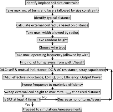
2.6 Flowchart of the inductor modeling design flow. . . 20
2.7 Physical dimensions of the coils (for both systems). . . 23
2.8 (a) Efficiency versus unloaded quality factors Q2 and Q3 (Q1 = 1.61, Q4 = 0.06). (b) Efficiency versus loaded quality factors Q1 and Q4 (Q2 = 6422, Q3 =277,k23 =0.01). . . 24
2.9 Efficiency and output power versus operating frequency (at coil distance=50mm). 25 2.10 Efficiency versus coil distance and operating frequency. . . 26
2.11 UnloadedQ2 versus operating frequency with different number of layers. . . 26
2.12 Q2andS RF2 versus number of turns per layer. . . 27
2.13 Coil 2 SRF versus number of turns and number of layers. . . 28
2.14 PTE versus distance for 2–coil and four–coil systems. . . 29
3.1 Lumped equivalent circuit of the inductor. . . 33
3.2 Electrical model for the power transfer system. . . 33
3.3 (a) 3D plot for PDL versus coil distance and number of turns. (b) 2D plot for PDL versus coil distance for up to 8 number of turns. . . 35
3.4 PTE versus coil distance for several number of turns. . . 36
3.5 PTE versus coil distance for different source resistances. . . 36
3.6 Input power, output power, and efficiency of System 1. . . 37
3.7 Input power, output power, and efficiency of System 2. . . 37
3.8 Power harvesting unit with rectifier and voltage regulator blocks. . . 38
3.9 Output power versus time for different values ofRval. . . 39
3.10 The charge pump unit. . . 40
3.11 Output voltage versus time for different values ofVin. . . 40
3.12 Block diagram of overall system: external and internal sub–blocks. . . 41
4.1 Cross–section of two non–coaxial and non–parallel circular coils, where the secondary coil is a thin disk coil, represented by a single filamentary coil. . . . 47
4.4 (a) Coupling coefficientk23 versus angular separation θfor different coil
dis-tancesc(axial misalignmentd is 0). (b) Coupling coefficientk23 versus axial
distancedfor different coil distancesc(angular misalignmentθis 0). . . 52
4.5 Sensitivity analysis ofk23with respect to both axial and angular misalignments (c=50mm). . . 53
4.6 Flowchart to find worst–case alignment of primary and secondary coils. . . 54
4.7 Typical subject (mouse) with implanted telemetry system powered by external coil. . . 55
5.1 2D coil setup in COMSOL andcoarsertriangular mesh. . . 60
5.2 Magnetic flux density (normal) and electric field (normal). . . 61
5.3 Coil setup with the secondary coil being misaligned, and its 3D rendition (view at 225◦revolution). . . 62
5.4 Electric field (normal) at 12.80MHzshowing noise. . . 63
5.5 3D coil setup in COMSOL andcoarsetriangular mesh. . . 65
5.6 Electric potential and magnetic flux density (normal). . . 66
5.7 (a) Mutual inductance versus coil distance. (b) Mutual inductance versus pri-mary coil radius (coil distance=50mm). (c) Mutual inductance versus axial misalignment (coil distance=50mm). (d) Mutual inductance versus angular misalignment (coil distance=50mm). . . 68
5.8 3D coil model in EMPro. . . 70
5.9 Simulated S-parameters of the EMPro model. . . 72
2.1 Parameters chart of Litz wire (individual strands) . . . 16 2.2 Coils’ physical and electrical specifications: 40 strand AWG44 (f=850kHz) . . 22 2.3 Coils’ physical and electrical specifications: 105 strand AWG48 (f=2.8MHz) . 22 4.1 Detailed sequence of MATLAB functions used in the optimization process
(Part 1) . . . 50 4.2 Detailed sequence of MATLAB functions used in the optimization process
(Part 2) . . . 51 5.1 Comparison between theoretically calculated and FEM simulated parameter
values . . . 62 6.1 Comparison of this research with other similar works . . . 78
Nomenclature
WPT Wireless Power Transfer
ICPT Indcutively–Coupled Power Transfer
RF Radio Frequency
EM Electromagnetic
RFID Radio Frequency Identification Device
PTE Power Transfer Efficiency
FEM Finite Element Method
PSC Printed Spiral Coil
IC Integrated Circuit
CMOS Complementary Metal–Oxide–Semiconductor
SRF Self–Resonant Frequency
PCB Printed Circuit Board
PDL Power Delivered to the Load
SAR Specific Absorption Ratio
ESR Equivalent Series Resistance
KVL Kirchoff’s Voltage Law
RMS Root–Mean–Square
FDTD Finite–Difference Time–Domain
DC Direct Current
AC Alternating Current
IEEE The Institute of Electrical and Electronics Engineers
MPE Maximum Permissible Exposure
PEC Perfect Electric Conductor
CMT Coupled–Mode Theory
RLT Reflected Load Theory
Introduction
Interest for biomedical implantable devices is gaining momentum among both health profes-sionals and researchers since they offer a variety of applications. Examples of applications include automatic drug delivery systems, devices to stimulate specific organs, and monitors to communicate internal vital signs to the outer world. Though all of these devices perform different tasks, one of their common issues is that of power requirements, which is a widely researched area over the past decade.
Genetically engineered laboratory subjects under medical studies are often implanted with microsensors that are connected by transcutaneous wires. This technique guarantees a constant power supply and reliable data transmission of the recorded signals, while its main shortcoming is that it requires the subject to be under anesthesia and, therefore, fails to generate undistorted life–like physiological data of an untethered freely moving subject [2]. In addition, the size of the battery that is used as the power source is a limiting factor for the implant’s miniaturization and lifetime, while the battery itself requires periodical surgical replacement with possible adverse consequences on the subject such as infections. Hence, a wireless continuous power delivery system is a more suitable method for providing energy to the implants.
This chapter introduces the topic of the present research work. Section 1.1 provides a com-prehensive literature review on similar works till date. Section 1.2 presents the motivation
behind the work and the objectives of the research. Lastly, Section 1.3 describes the organiza-tional layout of this thesis.
1.1
Review on Inductive Power Transfer Links
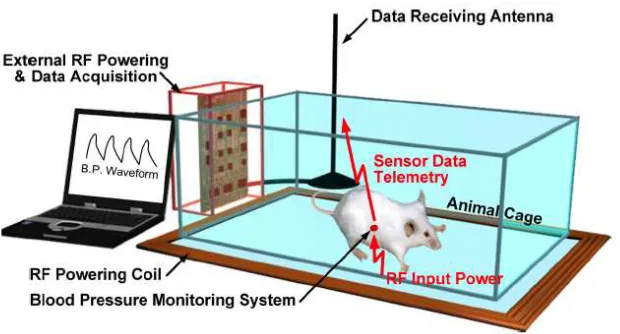
The first demonstration of wireless power transfer (WPT) dates back to 1899, performed by Nikola Tesla in Colorado Springs, Colorado [3]. In his experiment, 200 incandescent lamps were lightened when powered by a base station 26 miles away. A study on wireless monitoring systems was conducted in 1957, where development of endoradiosondes or radio–pills was carried out by [4]. In 1962, a passive echo capsule was also developed for similar purposes (pressure, temperature and pH sensing) by [5]. Since then several research projects have been undertaken in this field, including those that have been clinically evaluated, and whose power requirements vary with device application and can range from tens ofmicrowattsto hundreds ofmilliwatts[1], [6].
For implants designed for subjects such as genetically–modified laboratory mice, housing a battery within the implant would not be possible because of size limitations. The researchers in [7] have proposed wireless inductively–coupled power transfer (ICPT) solutions for their telemetry system designed for rats. Their implant uses a rechargeable battery which is charged when the alignment of the coil enables power transfer, and is discharged when it is misaligned. Unfortunately, this approach is not suitable for mice since the battery size would be too large (20mm diameter).
Figure 1.1: General layout of a wireless and batterylessin vivo bio–sensing microsystem by Conget.al.[1] cIEEE 2010
this technique was RF identification (RFID) tags [10], the same principle can be applied to sensor–based wireless biomedical implants [11].
Some latest research endeavors by [1] in 2009 have developed an implant that has a chip area of 2.2x2.2mm2and weighs 130mg and can be integrated with an artery of the mouse for blood pressure monitoring (Fig. 1.1). The specifications of the chip are ideal for laboratory mice implants given their arterial diameter of about 200um [12]. Since magnetic coupling theory enables efficient power transfer only when the magnetic field is perfectly aligned with the inductor, the challenge is to design a powering system that would work independent of the subject’s orientation. Such designs, which are mainly focused on the generation of constant minimum power from the floor of the subject’s cage, have been investigated in [13].
External Circuit
Implant Circuit
Figure 1.2: Typical setup of inductively coupled coils (with magnetic field shown).
effects of source and load resistance from the coils, and in this way achieve a high quality factor for them. This method is less sensitive to changes in the coil distance and typically employs two pairs of coils: one in the external circuit called driver and primary coils, and the other in the implant itself called secondary and load coils.
Most of the work in this area so far revolves around either static large radii coils for rela-tively high power transfer applications [14], or printed spiral coils (PSCs) used for low power integrated circuit (IC) implementations [16]. Some latest studies on wireless power transfer to implantable devices based on resonance–based inductive coupling with emphasis on their power transfer link efficiency are presented in [17], [18] and [19].
1.2
Motivation and Research Objectives
The aim of this research is to develop a design and optimization system for implementing wireless power transmission to small–size biomedical implants for freely–moving subjects. The system is not application–specific, and thus can be customized and implemented as per application requirements such as size and power.
defined as follows:
• To be able to completely eliminate the need for batteries in wireless biomedical implants for small–size living subjects, a resonance–based inductively–coupled power transfer system needs to be developed, that is capable of delivering the required power for the implant application (load) with maximum efficiency.
• A step–by–step design process needs to be developed for the modeling of the inductors to be used in the system, which will be able to automatize the development of the entire WPT system, and directly produce the parameter values with the help of specified design constraints and requirements.
• To begin the design procedure, a discrete–component circuit needs to be adopted us-ing the component values achieved from the previous step. Choices have to be made regarding the type of wire to be used for the inductor coils and the operating frequency.
• Optimization of the electrical parameters, which in turn optimizes the inductors’ physical specifications, in order to maximize Power Transfer Efficiency (PTE) and output power of the circuit needs to be performed.
• An analytical study on misalignment of the resonating coils need to be performed to identify the worst–case alignment scenarios. The analysis should be verified with mea-surements and Finite Element Method (FEM) electromagnetic modeling, preferably with the inclusion of real–life animal models.
1.3
Organization of the Thesis
The research thesis presents the design and optimization procedure for a wireless power trans-fer link for biomedical implants. It has been organized in the form of chapters that have been described below.
In Chapter 2, the modeling terms involved and optimization of the inductor coils for maxi-mum power transfer efficiency is presented, with the help of analytical results and discussion.
In Chapter 3, the resonance-based wireless power transfer circuit is thoroughly analyzed. Discussions on power requirements, the power harvesting circuit, and typical application sys-tems are also presented.
In Chapter 4, the misalignment of the inductor coils in real–life scenarios is analyzed, with various case descriptions and experimental results.
In Chapter 5, Finite Element Method (FEM) electromagnetic modeling of the inductors is conducted with the help of FEM–based software.
Inductor Modeling and Optimization
This chapter deals with the various modeling parameters required for the design of the inductor coils, such as, inductance, capacitance and resistance of the coils. Analytical models for each of the parameters are presented, which is followed by detailed analysis of the design flow and optimization of the entire resonance–based power–transfer system.
The inductor coil models are based on a multilayer helical structure wound around a plastic base using a special type of wire called the Litz wire. However, the design flow has been generalized to accommodate any inductor type that requires similar design parameters. This can be easily performed by changing the governing equation for the specific parameter.
As opposed to CMOS (Complementary Metal–Oxide–Semiconductor) coils, helical and spiral coils are only able to operate in a moderate frequency range of a few hundredkilohertz
to a few megahertz since they have a larger size and a lower self–resonant frequency (SRF) due to high parasitic capacitance. However, they are able to achieve a higher self–inductance, thus an unconstrained quality factor and a better efficiency profile with respect to a carefully– designed compact and optimized size. We will investigate details of the previous statement in following sections of the thesis.
B-field
Figure 2.1: Basic inductor showing current and magnetic field.
2.1
Overview
An inductor is defined as a passive electrical component with two terminals. In contrast to ca-pacitors, which store energy in their electrical fields, the inductor stores energy in its magnetic field. Typical inductors are made of a wire or other conductive material wound into a coil, in order to amplify the magnetic field.
Inductance can be described using Faraday’s law of electromagnetic induction coupled with Lenz’s law. The basic definition states that when the current flowing through an inductor changes, a time–varying magnetic field is created inside the coil, and a voltage is induced, which opposes the change in current that created it (Fig. 2.1). Therefore, inductors are classical components used in electronics where current and voltage vary with time, due to the their ability to change the phase of alternating currents.
2.2
Modeling Terms
Although different choice of equations are available for modeling inductors, the terms involved in complete modeling for our study and application are analytically described in this section.
2.2.1
Mutual Inductance
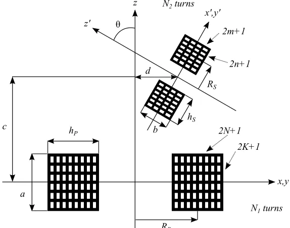
The mutual inductance of a pair of current–carrying coils is the amount of magnetic flux linkage between them. The mutual inductance is a strong function of the coil geometries and the distance between them. For two non–coaxial and non–parallel filamentary coils, the mutual inductance is [20]
M = µ0
π p
RPRS
π
Z
0
(cosθ− d
RScosφ)Ψ(k) √
V3 dφ (2.1)
where
V =
s
1−cos2φsin2θ−2 d
RS
cosφcosθ+ d
2
R2
S
,
k2 = 4αV
(1+αV)2+ξ2, ξ = β−αcosφsinθ, Ψ(k)= 2
k −k
!
K(k)− 2
kE(k), α= RS
RP
, β= c
RP
.
φ angle of integration at any point of the secondary coil;
RP radius of the primary coil;
RS radius of the secondary coil;
c distance between coil centers;
d distance between coil axes;
θ angle between coil planes;
K(k) complete elliptic integral of the first kind [21]; E(k) complete elliptic integral of the second kind [21];
The above mutual inductance expression (2.1) assumes that the primary coil radius RP is
larger than the secondary coil radius RS. It is the most general case, for when the angular
misalignmentθ or the axial misalignmentd is set to zero in the equation (2.1), it takes more simplified forms.
For our case of multilayer helical coils with axial and angular misalignment, we apply the filament method [22] to (2.1) to calculate the mutual inductance of the entire coil, which produces the following equation [20]:
M = N1N2
g=K
P
g=−K h=N
P
h=−N l=n
P
l=−n p=m
P
p=−m
M(g,h,l,p)
(2S +1)(2N+1)(2m+1)(2n+1) (2.2)
where
M(g,h,l,p)= µ0
π p
RP(h)RS(l) ×
π
Z
0
[cosθ− Ry(p)
S(l)cosφ]Ψ(k)
√
V3 dφ,
V =
s
1−cos2φsin2θ−2y(p)
RS
cosφcosθ+ y
2(p)
R2
S
,
k2 = 4αV
(1+αV)2+ξ2, ξ = β−αcosφsinθ, Ψ(k)= 2
k −k
!
K(k)− 2
kE(k), α= RS
RP(h)
, β= z(g,p)
RP(h)
,
y(p)= d+ bsinθ
(2m+1)p; p= −m, ...,0, ...,m
RP(h)= RP+
hP
(2N+1)h; h=−N, ...,0, ...,N
RP =
R1+R2
2 ; hP =R2−R1;
RS(l)= RS +
hS
(2n+1)l; l=−n, ...,0, ...,n
RS =
R3+R4
2 ; hS = R4−R3;
z(g,p)=c+ a
(2K+1)g+
bcosθ (2m+1)p;
a
hP
hS b
RP
RS
c
d
θ
x,y x',y'
z z'
2m+1 2n+1
2K+1 2N+1
N1 turns N2 turns
Figure 2.2: Cross–sectional view of two non–coaxial and non–parallel circular coils.
N1 number of turns in primary coil;
N2 number of turns in secondary coil;
a height of the primary coil cross–section;
b height of the secondary coil cross–section;
hP width of the primary coil cross–section;
hS width of the secondary coil cross–section;
R1 inner radius of the primary coil of rectangular cross–section;
R2 outer radius of the primary coil of rectangular cross–section;
R3 inner radius of the secondary coil of rectangular cross–section;
R4 outer radius of the secondary coil of rectangular cross–section.
2.2.2
Self Inductance
The self inductance of a current–carrying coil is the amount of magnetic flux through the cross– sectional area that it encloses. Formulas for finding the self inductance of an inductor coil, such as the planar spiral coil, the helical coil and the printed spiral coil, have been developed, like the ones shown in [16], [23], [24] and [25]. However, this thesis shows how the same equations used for finding the mutual inductance, (2.1) and (2.2), can be modified to produce the self inductance value for each of the coils.
First, we assume that M is equivalent to Ln, where n = 1,2,3,4, representing the four
inductors. Next, we makeaandbas half of the actual height of the coil, andhPandhS as half
of the actual width of the coil. We makec =a =b, d= 0 andθ =0, since there is technically no gap and misalignment between the coils (it is the same coil). Finally, we makeRP =RS and
N1 = N2.
With the above modifications, the same equations (2.1) and (2.2) are applied to find the self inductance values of the four coils. An important term binding the self and mutual inductance values is the coupling coefficient k, whose value can range from 0 to 1. When L1 and L2 are
the self–inductance of the two coils,M12andk12are related by
M12 =k12
p
L1L2 (2.3)
2.2.3
Parasitic Capacitance and SRF
Csel f = 1 N2
Cb(Nt−1)Na+Cm
Nt X
i=1
(2i−1)2(Na−1)
(2.4)
whereN is the total number of turns,Cbis the parasitic capacitance between two nearby turns
in the same layer, andCmis the parasitic capacitance between two different layers. For a tightly
wound coil,CbandCmare formulated as follows:
Cb =0r
π/4
Z
0
πDir0
ς+rr0(1−cosθ)
dθ (2.5)
Cm= 0r
π/4
Z
0
πDir0
ς+rr0(1−cosθ)+0.5rh
dθ (2.6)
where Di, r0, ς, r and h are the average diameter of the coil, wire radius, strand insulation
thickness, relative permittivity of strand insulation and separation between each layer respec-tively [28].
The parasitic capacitance and the self–inductance determine the self–resonant frequency (SRF) of the inductor as
fsel f =
1 2πpLCsel f
(2.7)
2.2.4
AC Resistance
At high frequencies, skin and proximity effects increase the effective series resistance (ESR), which decreases the quality factor of the inductor coils. In order to reduce its AC resistance, the coils are commonly made by using multistrand Litz wire [28], [29]. Finite–difference time–domain (FDTD) techniques are used to model AC resistance numerically in [30]. Semi– empirical formulation using finite–element analysis (FEA) is presented in [31]. The AC resis-tance of these coils, including skin and proximity effects, is found by [32]
Rac =
H+K NDI DO
!2 DI √ F
10.44
4
10−2 10−1 100 101 102 0.2
0.4 0.6 0.8 1
Ratio of h/w (height over width)
Area Efficiency
Figure 2.3: Area efficiency of coil (η) versus coil aspect ratio (h/w).
where
Rdc=
RS(1.015)NB(1.025)NC
NS
(2.9)
H resistance ratio of individual strands when isolated (Table 2.1);
F operating frequency in Hz;
N number of strands in the cable;
DI diameter of the individual strands over the copper in inches;
DO diameter of the finished cable over the strands in inches;
K constant depending on N (1.55< K <2);
Rdc resistance in Ohms/1000ft.;
RS maximum DC resistance of the individual strands;
NB number of bunching operations;
NC number of cabling operations;
NS number of individual strands.
Rac =Rdc 1+ f2 f2 h ! (2.10)
where fh is the frequency at which power dissipation is twice the DC power dissipation and is
calculated using the graph in Fig. 2.3 [28].Rdcis given by
Rdc = i=1
X
Na
πNtDiRul (2.11)
where Na is the number of layers, Nt is the number of turns, Di is the diameter of each layer
andRul is the DC resistance of the unit–length Litz wire.
2.2.5
Quality Factor
The total impedance of the inductor after considering the parasitic capacitance and AC resis-tance is given by [33]
Zt =(jωLsel f)+Rac k
1
jωCsel f
(2.12)
Therefore, the coil can be modeled with an effective inductance Le f f and an effective series
resistance ESR as
Le f f =
Lsel f
(1−ω2L
sel fCsel f)
(2.13)
ES R= Rac
(1−ω2L
sel fCsel f)2
(2.14)
An increase in the operating frequency towards the self–resonance frequency (SRF) increases the ESR drastically, and for a frequency higher than the SRF, the coil starts to behave as a capacitor (from (2.13)). The quality factor of the unloaded inductor is given by
Qunloaded =
ωLe f f
ES R =
2πf Lsel f(1− f2
f2
sel f
)
Rdc(1− f2
fh2)
(2.15)
Table 2.1: Parameters chart of Litz wire (individual strands)
Recommended Frequency Nominal Diameter Max. DC Resistance Single Strand
Wire Gauge Range over Copper (inch) (Ohms/m) Rac/Rdc“H”
28 AWG 60 Hz to 1 kHz 0.0126 66.37 1.0000
30 AWG 1 kHz to 10 kHz 0.0100 105.82 1.0000
33 AWG 10 kHz to 20 kHz 0.0071 211.70 1.0000
36 AWG 20 kHz to 50 kHz 0.0050 431.90 1.0000
38 AWG 50 kHz to 100 kHz 0.0040 681.90 1.0000
40 AWG 100 kHz to 200 kHz 0.0031 1152.30 1.0000
42 AWG 200 kHz to 350 kHz 0.0025 1801.0 1.0000
44 AWG 350 kHz to 850 kHz 0.0020 2873.0 1.0003
46 AWG 850 kHz to 1.4 MHz 0.0016 4544.0 1.0003
48 AWG 1.4 MHz to 2.8 MHz 0.0012 7285.0 1.0003
2.3
Litz Wire and Operating Fequency
The term litz wire originates from Litzendraht, German for braided/stranded wire or woven wire. It is a type of cable used in electronics to carry alternating current. The wire is designed to reduce the skin effect and proximity effect losses in conductors used at high frequencies. It consists of many thin wire strands, individually insulated and twisted or woven together, following one of several carefully prescribed patterns often involving several levels (groups of twisted wires are twisted together, etc.). This winding pattern equalizes the proportion of the overall length over which each strand is at the outside of the conductor [34].
Analytical models of winding losses in the Litz wire are presented in [35] and [36]. Table 2.1 [32] gives an overview of the parameters used for determining the type of the Litz wire, such as the operating frequency, diameter and resistance. For our purpose of wireless power transfer, the ideal frequency range of operation is from 100kHzto 4MHz, where no biological effects have been reported, in contrast to the extreme–low–frequency band and the microwave band [17]. This restricts our choice of wire from AWG40 to AWG48 (Table 2.1).
2.4
Power Transfer E
ffi
ciency
However, it has a direct relationship with theQ–factor of the coils and their coupling coefficient
k. For a four–coil system, PTE is given by [17] [37]
η= k12k23k34
√
Q1Q2
√
Q2Q3
√
Q3Q4
√
R1R4[(1+k212Q1Q2)(1+k234Q3Q4)+k232 Q2Q3]
(2.16)
Higher Q–factor of the coils and good coupling between them, and lower source and load resistance, yield higher PTE values for the circuit. For resonant–based structures, the low– Q of the driver and load coils (due to the series source resistance of the driver coil, and the load resistance and small size of the load coil) are compensated by the high–Q of the primary and secondary coils, and good coupling between the driver and primary coils (k12), and the
secondary and load coils (k34).
Efficiency does not vary much with respect to the driver coil’sQ–factor and has a maxima for the load coil’s low Q–factor [17]. An optimum set of physical and electrical parameters exist for the highest efficiency for each design. This is researched in the following sections.
2.5
Design Flow and Optimization
It is a challenging task to determine direct correlations between physical/electrical parameters and performance parameters such as quality factor and power transfer efficiency because of the number of interrelated intermediate parameters in the design process. Changing a certain physical parameter may influence more than one intermediate parameter, all of which in turn affect a particular performance parameter in different ways. Therefore the trend achieved is due to a combination of effects, rendering the direct effect obscure.
1 2 3 4 5 6 1 2 3 4 5 6
1 2 3 4 5 6
1 2 3 4 5 6 12 11 10 9 8 7
12 11 10 9 8 7 13 14 15 16 17 18
13 14 15 16 17 18 24 23 22 21 20 19
24 23 22 21 20 19 25 26 27 28 29 30
25 26 27 28 29 30 Mechanical Plastic Base
Driver or Load Coil
Wire Cross-Section
Primary or Secondary Coil
Turn Index
Side Walls
Individual Strand
Litz Wire Cross-Section
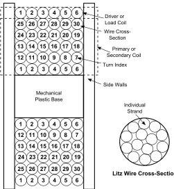
Figure 2.4: Structure of the inductor coils and Litz wire.
• The driver and primary coil pair in the circuit is realized with the help of a plastic base around which the Litz wire is wound (Fig. 2.4). The driver coil is wound above the primary coil concentrically. Similar approach is taken for the secondary and load coils. This is done in order to simplify the structure and maximize the coupling coefficient.
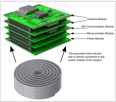
• The radius of the implant coil is chosen as per constraints of the implant size. The focus of our project is to supply power to a biological implant that is meant to be embedded inside the body of a living subject. The current implant design consists of four PCB boards of 15x15mm2area connected vertically, one of which is the power board that will house the secondary–load inductor pair with approximate diameter of 15mm(Fig. 2.5).
Power Module
Microcontroller Module RF Communication Module
Interface Module
The secondary-load inductor pair is directly connected to the power module of the implant
Figure 2.5: The implant PCB boards demonstrating where the inductor is connected.
the relationshipouter diameter= distance2√2 [38] from the equation [16]
H(x,r)= I.r
2
2p(r2+x2)3 (2.17)
where H is the magnetic–field strength in a single–turn circular coil with radius r at a distancexalong the axis, and maximizes when the above relationship is true.
• It is either the chosen wire type that will dictate the operating frequency or a pre– determined operating frequency that will help choose the type of wire. The sequence of these two choices can be decided by the designer.
Identify implant coil size constraint
Take max. no. of turns and layers (allowed by size constraint) Identify typical distance
Calculate external coil radius based on distance Take max. width allowed by radius
Take random height Choose wire type
Take max. operating frequency (allowed by wire) Find no. of turns/layers from width/height
CALC: self & mutual inductance, DC & AC resistance, stray capacitance CALC: effective inductance, ESR, Q, SRF, Efficiency, Output Power
Sweep frequency to maximize efficiency
Sweep external coil height to maximize Pload at desired distance
Is SRF at least 4 times f? Decrease no. of turns/layers
Proceed to simulations/measurements No
Yes
Figure 2.6: Flowchart of the inductor modeling design flow.
and power requirements [39]. Therefore we choose the AWG44 and AWG48 wire types, whose operating frequency range are 350–850kHz and 1.4–2.8MHz respectively [32]. In order for the two systems to be directly comparable and the same dimensions of the implant inductor coil to be re–used, the two wire configurations are selected with approximately the same diameter, 0.48mm. Therefore, the AWG44 wire has 40 strands (single strand diameter = 0.05mm) and the AWG48 wire has 105 strands (single strand diameter=0.0305mm).
2.5.1
System 1
We closely follow all the specified design steps of the optimization process in Fig. 2.6 for creating this system of inductors. Firstly, all the design constraints are chosen according to the implant’s application criteria. The implant coil diameter is chosen as 15mmas mentioned earlier. The Litz wire (40 strand AWG44) is approximately half a millimeter in thickness. Therefore, we make the topmost layer, which is the load coil, have an inner diameter of 14mm, thereby making the outermost diameter of the coil very close to, but not above, 15mm.
Thereafter, the rest of the inner space is left for the secondary coil winding. Twelve layers can be accommodated, that leaves an small internal 2.24mm space to place the base of the plastic spool. We recommend the overall height of the coil not to go over 5mmfor maintaining compactness of the designed implant. Therefore, the number of turns is 9 for the secondary– load coil pair, which gives a wire–only height of 4.41mm.
Since the typical distance between the external and implant coil is taken as 50mm, equation (2.17) produces an average external coil radius of 35mm, which is chosen. Once again, the driver coil is placed as the outermost layer. The maximum number of layers that can be allowed for the primary coil is 82, which leaves an internal space of 5.22mmfor the spool base. The number of turns for the driver–primary coil pair is first chosen randomly but later on dictated by the optimization of the power delivered to the load (described in Chapter 3).
The next step is to chose the type of wire, which has been explained previously. This gives us the operating frequency limits. Now we are able to calculate all the electrical parameters of the inductors. This is followed by sweeping of the operating frequency in order to maximize the power transfer efficiency, sweeping of the primary coil height to maximize the actual delivered power, and lastly, checking if the self–resonant frequency of the the coils is within the limit.
This system’s physical and electrical specifications are given in Table 2.2. Using the MATLABR code given in Chapter 4.2, the calculations of the modeling terms are performed
Table 2.2: Coils’ physical and electrical specifications: 40 strand AWG44 (f=850kHz)
Coil Type Outer Dia. Inner Dia. Turns per No. of Height of
(mm) (mm) Layer Layers Base (mm)
Driver 1 136.36 134.78 2 1 0.98
Primary 1 134.78 5.22 2 82 0.98
Secondary 1 14 2.24 9 12 4.41
Load 1 14.98 14 9 1 4.41
Coil Type Inductance (calc.) Inductance (sim.) Capacitance Self–Resistance Q–factor
Lself (µH) Lself (µH) Cself (f F) Rac(Ω) (unloaded)
Driver 1 1.76 1.83 40.09 0.22 43
Primary 1 2012 2001 0.31 0.83 12946
Secondary 1 46.85 47.13 2.66 0.31 807
Load 1 0.45 1.06 1.67 0.10 24
From the calculations, the maximum power transfer efficiency is found to be 77.13% at 50mm coil distance and 850kHz operating frequency, using the optimized parameters. The various parameter trends observed while designing this system and the conclusions drawn from them have been discussed in Section 2.6.
2.5.2
System 2
Modeling of this system is similar to that of the previous system. The implant coil dimensions are identical since the implant structure is the same. However, since the Litz wire (105 strand AWG48) and operating frequency are different, the remaining steps of the design flow are also different. The primary coil width and thus the number of turns is restricted to 15, because the self–resonant frequency limit is reached sooner for the higher operating frequency (2.8MHz).
Table 2.3: Coils’ physical and electrical specifications: 105 strand AWG48 (f=2.8MHz)
Coil Type Outer Dia. Inner Dia. Turns per No. of Height of
(mm) (mm) Layer Layers Base (mm)
Driver 2 83.43 81.85 2 1 0.98
Primary 2 81.85 58.15 2 15 0.98
Secondary 2 14 2.24 9 12 4.41
Load 2 14.98 14 9 1 4.41
Coil Type Inductance (calc.) Inductance (sim.) Capacitance Self–Resistance Q–factor
Lself (µH) Lself (µH) Cself (f F) Rac(Ω) (unloaded)
Driver 2 0.98 0.99 24.63 0.12 144
Primary 2 108.03 105.22 1.78 1.21 4579
Secondary 2 46.85 47.13 2.66 0.18 1571
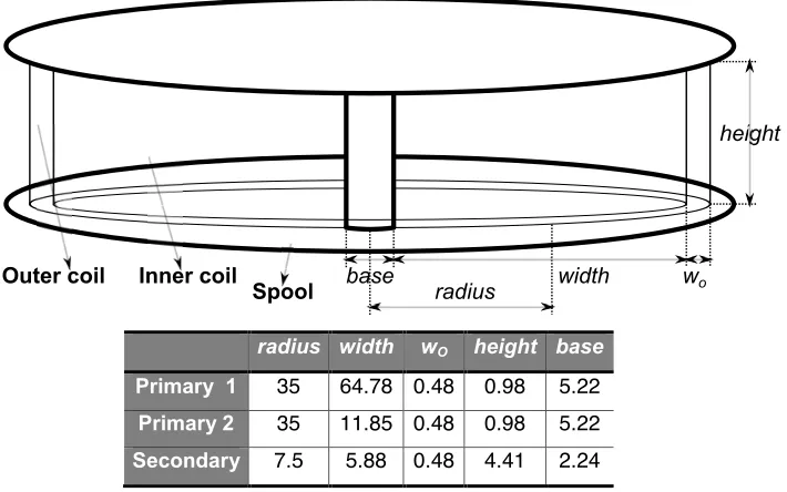
base width radius
height
wo Outer coil Inner coil
Spool
radius width wO height base
Primary 1 35 64.78 0.48 0.98 5.22
Primary 2 35 11.85 0.48 0.98 5.22
Secondary 7.5 5.88 0.48 4.41 2.24
*all dimensions are in millimeters
Figure 2.7: Physical dimensions of the coils (for both systems).
The maximized power transfer efficiency for this system is80.66%at 50mmcoil distance and 2.8MHz operating frequency. This system has the physical and electrical specifications given in Table 2.3.
Figure 2.7 shows the dimensions for all the coils designed for the two systems. As expected, both the systems have peak efficiencies at 50mm, which is the distance that they were optimized for by using the external coil diameter. However, this study has proven that fine–tuning of the actual peak output power (or power delivered to the load PDL) for a certain coil distance is possible but requires other parameter choices to be taken into consideration.
2.6
Results and Analysis
2.6.1
Quality Factor of Coils
The Litz wire has been chosen to achieve a low AC resistance and a high quality factor at a specific operating frequency. Litz wires do not offer extremely high frequencies (only up to a couple of MHz), but we would not prefer anything higher than 4MHzanyway, since human and animal tissue has a lower specific absorption rate (SAR) for low–frequency RF signals compared to the high–frequency signals.
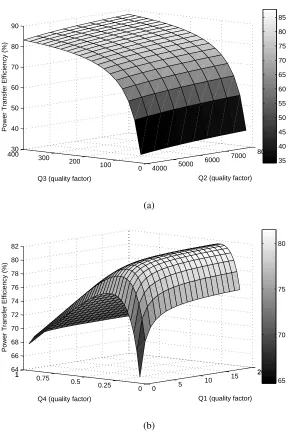
4000 5000 6000 7000 8000 0 100 200 300 40030 40 50 60 70 80 90
Q2 (quality factor) Q3 (quality factor)
Power Transfer Efficiency (%)
35 40 45 50 55 60 65 70 75 80 85 (a) 0 5 10 15 20 20 0 0.25 0.5 0.75 1 1 64 66 68 70 72 74 76 78 80 82
Q1 (quality factor) Q4 (quality factor)
Power Transfer Efficiency (%)
65 70 75 80
(b)
Figure 2.8: (a) Efficiency versus unloaded quality factorsQ2 andQ3 (Q1 = 1.61, Q4 = 0.06).
200 400 600 800 1000 1200 0
20 40 60 80 100 100
Frequency (kHz)
Power Transfer Efficiency (%)
200 400 600 800 1000 12000
40 80 120 160 200 200
Power Delivered to Load (mW)
PTE PDL
Figure 2.9: Efficiency and output power versus operating frequency (at coil distance=50mm).
Also, the small–size implant coil has a small inductance and parasitic capacitance, which means a lower frequency of operation will require a high capacitance value for the external tuning capacitor, thus rendering the capacitance due to tissue effects negligible. Lastly, because of the self–resonant frequency (SRF) constraint of the coil, the operating frequency is needed to be kept low in order to avoid high effective series resistances (ESR). All of the above reasons help us achieve high unloaded quality factors for Coil 2 and 3, as can be observed in Fig. 2.8(a). The loaded quality factors of the driver and load coils are restricted by the source and load resistances. TheQ–factor of Coil 4 is very low due to the high load resistance (ranging from 100Ωto 1kΩ) and small implant size, and theQ–factor of Coil 1 is moderate due to the large size of the external coil. However, the efficiency peaks at a certainQ4value, and remains quite
constant with some variation inQ1values, as can be observed in Fig. 2.8(b).
2.6.2
Operating Frequency Variation
0 20 40 60 80 100 0 250 500 750 1000 10000 10 20 30 40 50 60 70 80
Coil Distance (mm) Operating Frequency (kHz)
Power Transfer Efficiency (%)
10 20 30 40 50 60 70
Figure 2.10: Efficiency versus coil distance and operating frequency.
200 300 400 500 600 700 800 900 1000 1100 1200 0 500 1000 1500 2000 2500 3000 3500 Frequency (kHz)
Unloaded Quality Factor (Q2)
5 layers 15 layers 25 layers 35 layers 45 layers 55 layers 65 layers 75 layers
Figure 2.11: UnloadedQ2versus operating frequency with different number of layers.
Fig. 2.9 and Fig. 2.10 show this phenomenon of relative immunity to operating frequency from 400kHz to 1200kHz. However, the output power (PDL) in Fig. 2.9 decreases with in-creasing frequency because maximum power can only be delivered to the load when half of the power is dissipated at the source, meaning the efficiency is 50%. This happens at around 300kHzin the graph. In Fig. 2.10, the variation of the power transfer efficiency with the coil distance is also observed, with peak efficiency being at 50mm, as anticipated.
0 2 4 6 8 10 12 14 16 18 20 2000
4000 6000 8000 10000 12000
Number of Turns
Quality Factor (Q2)
0 2 4 6 8 10 12 14 16 18 200
2000 4000 6000 8000 10000
Self−Resonant Frequency (kHz)
SRF2 Q2
Figure 2.12:Q2andS RF2 versus number of turns per layer.
2.6.3
Choice of Primary Coil Parameters
As mentioned earlier, the primary coil size is the determined by the typical distance where efficiency needs to be maximum, which is why we have chosen a radius of 35mm for a coil distance of 50mmbased on (2.17).
For the optimization process to be successful, in System 1, we have used 82 layers for the primary coil with which the self–resonant frequency SRF is still reasonable (6.4MHz, which is almost 8 times greater than the operating frequency of 850kHz). Going above 82 layers would physically require the coil to have a larger radius, which would in turn change the fine–tuning of the peak efficiency to 50mm. For the primary coil in System 1, the width of the plastic base is kept at a minimum of 5.22mm, for the spool to be architecturally sound.
For System 2, we have kept the primary coil radius the same because of similar design con-straints. However, the number of layers Nais decreased to 15, because of the SRF constraint.
For this system, we have a primary coil SRF of 11.5MHz, which is more than 4 times larger than the operating frequency of 2.8MHz.
For the choice of the number of turnsNt, the determining factor is the output power (PDL)
2 4
6 8
10
10 20 30 40 50
0 2000 4000 6000 8000 10000 12000
Number of Turns Number of Layers
Coil 2 Self−Resonant Frequency (kHz)
2000 4000 6000 8000 10000 12000 14000
Figure 2.13: Coil 2 SRF versus number of turns and number of layers.
more than 6, which is also true for the SRF. However, both have a steep curve up to 6 turns. The 3D plot in Fig. 2.13 shows the combined effect of change inNtandNaonS RF2. It can be
observed that an increase inNadoes not drastically reduce the SRF, but rather causes it to have
a gradual response.
2.6.4
Two–Coil versus Four–Coil Systems
The aim of the resonance–based four–coil system is to avoid the problems observed in the two– coil system, mainly the drastic monotonic decrease of the the power transfer efficiency with an increase in coil distance due to the low coupling coefficient between the primary and secondary coils. Fig. 2.14 clearly demonstrates this. It also shows the pre–determined efficiency peak and the relative immunity of the four–coil PTE for a wide range of coil distances.
2.7
Concluding Remarks
0 10 20 30 40 50 60 70 80 90 100 0
10 20 30 40 50 60 70 80 90
Distance (mm)
Power Transfer Efficiency (%)
2−coil 4−coil
Figure 2.14: PTE versus distance for 2–coil and four–coil systems.
process for maximizing the power transfer efficiency (PTE) in a four–coil system, and demon-strated the various design constraints, choices and trends observed during the design flow.
Power Transfer Circuit
Although coupled–mode theory has been originally used to to describe resonance–based cou-pling, it can also be transformed into a simple circuit–based model. This chapter explains the physics behind resonance–based power transfer and discusses various details of the system design, such as electrical parameter choices, power harvesting, and application systems. The power transfer circuit is designed using discrete components that are chosen in accordance to the specifications of the modeled inductors in the previous chapter.
3.1
Resonance–Based Power Transfer
In 2008, the authors in [40] have investigated and established a non–radiative scheme that can lead to strong coupling between two medium–range distant long–lived oscillatory resonant electromagnetic states with localized slowly–evanescent field patterns, that are practical for efficient medium–range wireless energy transfer.
Although this was the first significant attempt at the resonance–based approach after Nikola Tesla’s back in 1914, there have been other ways of wireless energy transfer for several pur-poses till date. These include the following:
• Radiative modes of omni–directional antennas that work well for information transfer but
are not suitable for energy transfer because of high wastage of energy into free space.
• Directed radiation modes, using lasers or highly–directional antennas, that can be effi -ciently used for energy transfer even for long distances (distances several times larger than the characteristic size of the transmitting device), but require existence of an unin-terruptible line-of-sight and a complicated tracking system in the case of mobile objects.
• Other non–radiative modes such as magnetic induction, but they are restricted to very close–range or very low–power energy transfers.
The resonance–based method is based on the fact that two same–frequency resonant objects tend to couple, while interacting weakly with other off–resonant environmental objects, and even more strongly where the coupling mechanism is mediated through the overlap of the non– radiative near–field of the two objects [40]. This resonant energy–exchange can be modeled by the appropriate analytical framework called coupled–mode theory (CMT) [15], and also by the reflected load theory (RLT) [41].
3.1.1
Coupled–Mode Theory
In this system, the field of the system of two resonant objects 1 and 2 is approximated by
F(r,t)≈a1(t)F1(r)+a2(t)F2(r) (3.1)
whereF1,2(r) are the eigenmodes of 1 and 2 alone, and then the field amplitudesa1(t) anda2(t)
can be shown to satisfy, to lowest order [15]:
da1
dt =−i(ω1−iΓ1)a1+iκa2, da2
dt = −i(ω2−iΓ2)a2+iκa1 (3.2)
whereω1,2are the individual eigenfrequencies,Γ1,2 are the widths due to the objects’ intrinsic
by 2κ; the energy exchange between the two objects takes place in time π/2κ and is nearly perfect, apart for losses, which are minimal when the coupling rate is much faster than all loss rates (κ >>Γ1,2). The desired optimal regimeκ/
√
Γ1Γ2 >> 1 is called the “strong–coupling”
regime, which is set as the figure–of–merit ratio for any wireless energy–transfer system, along with the distance over which this ratio can be achieved.
3.1.2
Reflected Load Theory
The authors in [41] have claimed that although CMT is a more physics–based approach and RLT is circuit–based, both the methods produce the same results for ICPT. However, CMT produces relatively simplified equations but works only for very low coupling and high-Qcoils. In the RLT method, the resistive loadRloadis transformed into a reflected load onto the primary
loop at resonant frequency. It has been shown that the highest PTE across such inductive links can be achieved when all LC–tanks are tuned at the same resonance frequency [29].
3.2
Circuit Specifications
The model for the resonance–based four–coil power transfer system consists of lumped equiva-lent circuits for the four inductors, referred to as driver, primary, secondary and load coils (also denoted as coils 1 to 4), as shown in Fig. 3.1. In the four–coil system, the high–Q primary and the secondary coils compensate for the low–Q of the source and load coils and the low coupling of the intermediate coils.
The coils are tuned to the operating frequency by varying the tuning capacitance Cn for
the given self–inductance as per the equationω= 1/√LnCn. For our example case, a voltage
source E of 10.2V is used. A source resistanceRsource of 50Ω and a resistor Rsense at 5.5Ω to
mimic the source resistance of a power amplifier are used in the first loop, as shown in Fig. 3.2. Lastly, a typical load resistance for implant circuitryRload at 100Ωis included in the last
Cself Rac Lself
Figure 3.1: Lumped equivalent circuit of the inductor.
L1 L2 L3 L4
R1 R2 R3 R4
Rsense Rsrc
C1 C2 k C3 C4
23
E
Rload
Figure 3.2: Electrical model for the power transfer system.
When circuit theory in the form of Kirchoff’s Voltage Law (KVL) is applied to the system, we achieve the following matrix that defines the relationship between voltage applied to the driver coil and current through each coil [17]:
I1 I2 I3 I4 =
Z11 Z12 Z13 Z14
Z21 Z22 Z23 Z24
Z31 Z32 Z33 Z34
Z41 Z42 Z43 Z44
−1 E 0 0 0 (3.3) where
Zmn =Rn+ jωLn+1/jωCn, form= n
= jωMmn, form, n
Coupling coefficientsk13, k24 andk14 are neglected due to the small size of the driver and
3.3
Input and Output Power
The ratio of the output power over the input power determines the power transfer efficiency. It is an extremely important parameter in wirelessly–powered biological implants because of safety issues and standards regarding tissue exposure to RF electromagnetic radiation [42]. Therefore, maximizing the efficiency will guarantee a relatively high power output at the load even with a relatively low power wave that has to travel through the body.
However, the optimization of the efficiency does not automatically optimize the output power. In cases where we are safely below the exposure limit, and we require a high power delivered to the load (PDL), we can choose to maximize it, even if it at the cost of a lower power transfer efficiency (PTE).
The matrix in (3.3) can be solved for various circuit parameters. For our purposes, we can solve it for the input power and the output power at load resistanceRload, which produces the
following equations:
Psource= EI1, Pload = I42Rload (3.4)
where E andRload are taken from the circuit’s example case as 10.2V and 100Ω respectively.
ReplacingI4, we can achieve the following version of the equation:
Pload=Rload
jω3M
12M23M34L2L3
√ L1L4E
√ L1L2
√ L2L3
√
L3L4(M212M342ω4+Z11Z22Z33Z44+ω2(M212Z33Z44+M232Z11Z44+M234Z11Z22))
2 (3.5)
0
50
100 0 5
10 15 20 0 50 100 150 200
Number of Turns Distance (mm)
Power Delivered to Load (mW)
20 40 60 80 100 120 140 160 180 (a)
0 20 40 60 80 100
0 50 100 150 200
Coil Distance (mm)
Power Delivered to Load (mW)
1 turn 2 turns 3 turns 4 turns 5 turns 6 turns 7 turns 8 turns (b)
Figure 3.3: (a) 3D plot for PDL versus coil distance and number of turns. (b) 2D plot for PDL versus coil distance for up to 8 number of turns.
3.3.1
E
ff
ect of Number of Turns on Peak Power
In contrast to the radius of the external inductor being used to tune the efficiency to a certain coil distance, the PDL tuning is dependent on the height (number of turns) of the external inductor. To demonstrate this, we have conducted a sweep for PDL versus number of turns for a range of coil distances, showed in Fig. 3.3(a) and 3.3(b).
0 20 40 60 80 100 0 15 30 45 60 75 90
Coil Distance (mm)
Power Transfer Efficiency (%)
1 turn 2 turns 3 turns 4 turns 5 turns 10 turns 15 turns 20 turns
Figure 3.4: PTE versus coil distance for several number of turns.
with increasing number of turns and for our typical coil distance of 50mm, we would require about 2 turns only to maximize PDL, which has been incorporated in our two system designs. From Fig. 3.4, it can be observed that the efficiency peak does not vary significantly with increasing number of turns and for a higher number of turns, the efficiency is quite uniform across the range of distances.
3.3.2
E
ff
ect of Source Resistance
As shown in Fig. 3.5, the source resistance does not have a significant effect on the power transfer efficiency. PTE peaks slightly higher and at a slightly smaller distance with a lowerRs.
0 20 40 60 80 100
0 10 20 30 40 50 60 70 80 90 Distance (mm)
Power Transfer Efficiency (%)
Rs=25Ohm Rs=50Ohm Rs=75Ohm Rs=100Ohm Rs=125Ohm Rs=150Ohm
0 20 40 60 80 100 10 15 20 25 30 Distance (mm) Power (dBm)
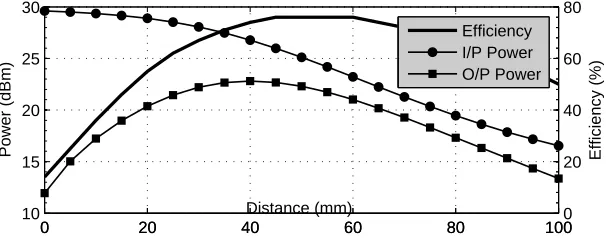
0 20 40 60 80 1000
20 40 60 80 Efficiency (%) Efficiency I/P Power O/P Power
Figure 3.6: Input power, output power, and efficiency of System 1.
0 20 40 60 80 100
−10 −5 0 5 10 Distance (mm) Power (dBm)
0 20 40 60 80 1000
20 40 60 80 Efficiency (%) Efficiency I/P Power O/P Power
Figure 3.7: Input power, output power, and efficiency of System 2.
3.3.3
Results
After performing the optimization of the output power, we have achieved high values for sys-tems 1 and 2 described in Chapter 2, that is shown in Fig. 3.6 and 3.7.
For the coils in System 1, a PDL of 22.3dBm has been achieved for 50mmcoil distance. For the high frequency coils in System 2, a PDL of 0.76dBmhas been achieved for the same distance. Therefore, our systems have been optimized in a way so that both PTE and PDL are maximized at the same distance between primary and secondary coils.
It is to be noted that for the System 2 circuit, we have chosen anRload value of 1kOhmand
8.08V 850kHz
C1=10uF
C2=10uF
Rload=100Ω R1=val
R2=1kΩ
Vin Output
Shdn' Adj
Figure 3.8: Power harvesting unit with rectifier and voltage regulator blocks.
3.4
Power Requirements and Harvesting Unit
So far we have only considered the transmission of power from the external circuitry to the implant coil. But the power in this form is not suitable for direct consumption by the implant. Therefore, we have designed a power harvesting circuit that rectifies and regulates the output power into a constant DC form.
Since the power requirements will vary as per the application of the implant, the power harvester circuit has been designed assuming a load resistance of 100Ωfor the architecture of System 1 in Chapter 2. This system has a voltage output of 8.08V at 850kHz, which is taken as the input voltage to the power harvesting circuit in Fig. 3.8.
The power harvester is entirely made up of discrete components. The system of diodes is a full–bridge rectifier or AC–to–DC converter. We have used the commonly–used D1N914 diode, which has a high switching speed and low forward voltage drop (≈ 0.6V). Any diode with similar rating can be used for the rectifier section. The capacitorC1 is for smoothing the
output waveform, and has been calculated using the following relations:
Vdc= Vac−2VD; r ≈
Vdc
2f C1Rload
(3.6)
whereVacis the AC input,Vdcis the DC output,VDis the forward voltage of the diode andris
0 0.1 0.2 0.3 0.4 0.5 0.6 0.7 0.8 0.9 1 0
100 200 300 400 420 500
Time (ms)
Output Power (mW)
R
val=100 Ohm R
val=250 Ohm R
val=400 Ohm R
val=550 Ohm R
val=700 Ohm R
val=750 Ohm
Figure 3.9: Output power versus time for different values ofRval.
Next we have a voltage regulator or DC–to–DC converter for forcing the output voltage to a certain constant value. For this purpose we have used the LT1121 micropower low dropout regulator with shutdown from Linear Technology. It has a dropout voltage of 0.4Vand a 150mA
output current.
Its four pins can be configured as per the requirements. The Shutdown pin has been shorted with theVin since we are not using that feature. The Output and and the Adjust pin have been
arranged as a potential divider so that the output voltage atRload can be adjusted by changing
the value of R1, thereby changing the R1/R2 ratio. Without the potential divider, the output
voltage would be a constant of 3.75V for this regulator.
The graph in Fig. 3.9 shows how the output power varies for different values of R1, and
saturates somewhere above R1 = 700Ω. The maximum power output that can be achieved
with this circuit for anR1of 750Ωor higher is 420mW, which is suitable for typical biological
implant applications.
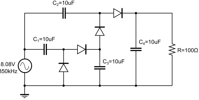
3.4.1
Charge Pump
C1=10uF
C2=10uF
C3=10uF
C4=10uF
8.08V 850kHz
R=100Ω
Figure 3.10: The charge pump unit.
0 50 100 150 200 250 300 350 400 450 500
0 5 10 15 20 25 30
Time (us)
Output Voltage (V)
V in=2.08V V
in=4.08V V
in=6.08V V
in=8.08V
Figure 3.11: Output voltage versus time for different values ofVin.
This charge pump is a typical variation of the Dickson’s charge pump [44]. The input voltage signal is offset by the shunt diode, and the resulting signal is then rectified by the series diode. By stacking a number of charge pump stages, the voltage signal can be multiplied to a much higher value, although adding too many stages also increases the parasitic capacitance of the diodes and the output impedance of the multiplier.
Power Source
End Device PC/Embedded
External
Unit
Internal
Unit
Power Harvesting
Unit
Microcontroller
RF Transceiver
Interface Electronics
Application Wireless Power
Transfer
Wireless Data Transfer 700 kHz
2.4 GHz
Figure 3.12: Block diagram of overall system: external and internal sub–blocks.
3.5
Typical Application Systems
Wireless power delivery can be used for numerous applications of modern autonomous elec-tronic devices such as cell phones, laptops and household robots. For our project, we are using it for implantable bio–sensors. This section presents a generic version of such a system, in order to demonstrate the functions of its various components [38].
The implantable system incorporates the receiver coils designed in the previous chapters. The overall system is divided into two units: external and internal (Fig. 3.12). The external unit includes both a power delivery section and an end device. The power delivery section contains a larger transmitting coil, which is connected to a wired power source, and is designed to allow for maximum power transfer to the smaller implant coil. The second sub–block is the end device, which can refer to a computer or a more application–specific embedded system. The end device is connected wirelessly to the internal unit through a wireless data–link (antenna).
bio–sensor data using a custom interface board and communicate it to the end device for further processing. The implantable unit contains three main sub–blocks, a power–harvesting block, a processing and transceiver block, and an application–specific interface block.
The power harvesting section of the internal system comprises of the inductor coil con-nected to other components to regulate and increase the reliability of the input power to the implant. Apart from the discrete component level power harvesting unit designed in Section 3.4, an Integrated Circuit (IC) level design of the power harvester has also been simulated in CMOS 0.13µmtechnology [43]. The design consists of a low–voltage low–power voltage regulator, which includes a charge pump and a temperature insensitive voltage reference.
The internal unit contains a microcontroller and an RF transceiver, that preferably have a low power consumption. The data is transmitted to the end device using Frequency Shift Keying (FSK) modulation at a frequency of 2.45 GHz. This allows the system to work in the Industrial, Scientific and Medical (ISM) band, which allows existing antenna technologies and devices to be used, while reducing developmental time and cost. Any signal processing and data compression is done in the microcontroller before it is sent to the end device.
The interface block of the implant includes bio–sensors that can be used for various ap-plications such as temperature and blood pressure monitoring. The interface electronics are custom to the application in order to reduce the power consumption of the system. Overlap-ping application areas may use the same or similar electronics, further reducing the size and power consumption of the system. The implantable system is able to be modified to be im-planted into lab subjects of various sizes and for different applications. Only modifications to the interface electronics and inductor design are required.
3.6
Summary
coupled–mode theory can be translated into a more circuit–based approach. The circuit speci-fications thoroughly define all the components of the power transfer block of the external and implant circuits, including the lumped equivalents of the four inductors. Circuit theory calcula-tions are used to derive direct relacalcula-tionships between output power and the inductor parameters, so that optimization of output power can be performed by reusing the procedure developed for efficiency optimization.
A novel relationship has been observed between the number of turns of the coil and position of the peak output power in Section 3.3.1. It shows that a greater number of turns shift the peak power to a smaller coil distance. This knowledge will enable future inductor designers to fine–tune their coils as per very specific application requirements. Also, the effect of source resistance on efficiency has been noted.
The results of the optimization procedure have been graphically demonstrated for the two systems described. System 1 has a PDL of 22.3dBm and System 2 has a PDL of 0.76dBm
for their respective specifications. Conclusions have been drawn on the optimal frequency for maximum output power.
In this chapter, a power harvesting unit and a charge pump have been designed to rectify, regulate and amplify the output voltage of the power transfer circuit. A power output of 420mW
Misalignment Analysis
Most of the studies conducted so far on wirelessly–powered biological implants deal with standard scenarios where the subject would be at a constant distance and/or position from the external circuitry. Some studies, such as [1] and [45] have addressed the issue of misalignment, but have not delved into it as far as the effects and boundaries of misalignment are concerned.
Therefore, in this thesis, we have conducted analysis and calculations on axial and angular misalignment of the primary and secondary coils, with conclusions on the feasibility of the power transfer circuit and allowable worst–case alignments of the two inductors.
4.1
Mutual Inductance with Misalignment
4.1.1
Overview
An inductive link can be compared to a loosely–coupled transformer for various electromag-netic applications, where the magelectromag-netic field generated by the primary coil is partially picked up by the secondary coil, thus enabling wireless power transfer. However, this system needs to be optimized for misalignment tolerance when the implant is meant for living biological subjects. Any misalignment directly affects the mutual inductance, which in turn reduces the overall power transfer efficiency.