High-Level Synthesis Of Inverse Quantization
And Transform Block For HEVC Decoder On
FPGA
Ahmed Ben Atitallah, Manel Kammoun
Abstract: This paper presents an efficient High-level synthesis (HLS) hardware design to implement the Inverse Quantization and Transform (IQ/IT) for a High Efficiency Video Coding (HEVC) decoder. Using Xilinx Vivado HLS tool, different directives are applied to the IQ/IT C code to select the optimized hardware architecture in terms of area and clock cycles. This architecture is implemented in a SW/HW context for verification. In fact, it is connected to ARM Cortex-A9 processor using AXI stream interface and integrated on Xilinx Zynq ZC702 platform. Therefore, the experimental results show that the SW/HW design can only decode 240p@15fps with a gain of 8% in throughput and 74% in power consumption compared to SW implementation.
Index Terms: HEVC Decoder; IDCT; Inverse quantization; HW/SW design, FPGA.
—————————— ◆ ——————————
1 INTRODUCTION
The HEVC standard [1][2] is the next generation codec successor to the previous standard (H.264/AVC, H.263, etc). In comparison to the last standard, HEVC delivers the same quality as H.264/AVC [3] at close to 50% of the bitrate, with a loss of 3 times in coding blocks complexity. Since the standardization of the HEVC decoder, there is a high demand for higher decompression rates in real-time [4]. Therefore, reduction of the computational complexity needs to develop a dedicated hardware designs for HEVC video decoder blocks. However, researchers have worked continuously to reduce this complexity by adopting hardware acceleration as a solution [5][6]. In this context, among the most complex blocks of the HEVC video decoder, we find the inverse quantization and the transformation (IQ/IT) which represent about 15% of computational complexity [7]. By appropriately designing the IQ/IT architecture, we can significantly reduce the time, energy and surface consumption [8]. Nowadays, commercial and academic HLS tools are started to be successfully used for the Field Programmable Gate Arrays (FPGA) implementations of complex algorithms. For example, Xilinx Vivado HLS [9], Intel OpenCL [10] and ROCCC [11] tools can generate hardware architecture from a C or C++ codes as input. The HLS advantages are the possible to simulate and explore several designs in the shortest time. Versus the manual implementation, the code structure in the HLS methodology can be automatically generated to make the control path. Indeed, the manual implementation needs a specifc data coding and control paths. Especially, for the complex video processing algorithms like as HEVC, the designing of the control path takes as much time and effort as building the data path [12][13]. In this context, the idea to use HLS for hardware implementation of the complex image and video processing algorithms are widely investigated since previous standards. Indeed, the approach proposed in [14] use the FOSSY synthesis tool to implement a full JPEG2000 decoder.
But, [15] proposes the implementation of the H.264/AVC decoder under Zynq 7045 FPGA using Xilinx Vivado HLS tool. The proposed design can decode 480p@34fps (frame per second). In [16] an FPGA design of 2D integer inverse discrete cosine transform (2D-IDCT) module using the Xilinx HLS tool is presented. This design is implemented on a Xilinx Virtex XC6VLX550T FPGA and can decode 1080p@54fps. However, our challenge in this paper is to design a hardware architecture based on the HLS design method for the IQ/IT algorithm supporting all HEVC Transform Unit (TU) sizes: 4×4 to 32×32 and validate it in software/hardware (SW/HW) environment. The benefit of the SW/HW implementation is that it enables the retention of the flexibility and accuracy of the SW while preserving the high performance of the HW. The remainder of the paper is organized as follows. the HEVC IQ/IT module is described in section II. the HLS optimization and implementation of the IQ/IT architecture is presented in section III. Section IV explores the experimental results of the SW/HW design in terms of, frame rate, area cost and power consumption for several video sequences using FPGA board. Finally, some concluding remarks are gathered in section V.
2 THE IQ/IT OVERVIEW
In HEVC, the IQ/IT is applied to the quantized transform coefficients resulting from the entropy decoding algorithm. However, the dequantization [17] process is first performed for all TU blocks of sizes 4×4, 8×8,16×16 and 32×32 pixels. The next step consists in applying the inverse transform. Indeed, HEVC standard specifies the 2D-IDCT for all TU blocks and the 2D integer inverse discrete sine transform (2D-IDST) for intra coded luminance transform blocks of size 4×4 pixels. The following equation defining the behavior of the 2D-IDCT [18] is given as follows:
Y= MT X M
(1)
where MT, X and Y are the transform block, the dequantized block and the result matrix (residual block), respectively, with sizes varying from 4×4 to 32×32 pixels. When the dequantized block is obtained, HEVC decoder performs 1D-IDCT/IDST to the rows and columns of TU to generate the 2D-IDCT/IDST transform matrix. The 1D-IDCT/IDST can be optimized for all ________________________________________
• Ahmed Ben Atitallah, Department of Electrical Engineering, Jouf University, Sakaka 2014, Aljouf, Saudi Arabia. LETI (E.N.I.S.), University of Sfax, Sfax, Tunisia. Email: [email protected] • Manel Kammoun, LETI (E.N.I.S.), University of Sfax, Sfax, Tunisia
1925
inverse transform matrices by using an even-odd decomposition [19]. Therefore, we exploit in this work the even-odd algorithm which is based on the symmetry properties between different matrices. However, this feature leads to realize hardware sharing between transform sizes. Fig. 1 describes our proposed decomposition method adopted for the partial butterfly of 32×32 matrix size. In fact, the even block of the 1D-IDCT32 is the same as that of the 1D-IDCT16. This property can be applied to the rest of transform sizes (4×4 and 8×8).
3 HLS
ARCHITECTURE
FOR
IQ/IT
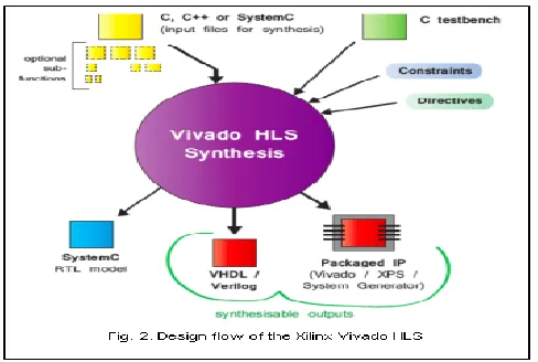
Fig 2. presents the design flow of the Xilinx Vivado HLS tools which uses C and C++ as programming languages for design description. From this description, the HLS tools can automatically generate the hardware architecture based on VHDL/Verilog languages. With Xilinx Vivado HLS some optimization options can be used to increase the hardware performance by applying several directives such as resource, loop unrolling, pipelining, etc. It allows to add specific RAM and ROM blocks to HLS implementation with directives. As well as, it permits to use the DSP blocks such as divider, multiplier or square unit in HLS design. It also has an option to choose the I/O ports as FIFO, memory, bus or acknowledge type. In addition, for data transfer, it allows to add high speed AXI4 busses such as AXI4-Lite and AXI4-Stream interfaces.
The purpose of this work is to investigate the HLS approach in SW/HW environment to design and verify a standalone IP of
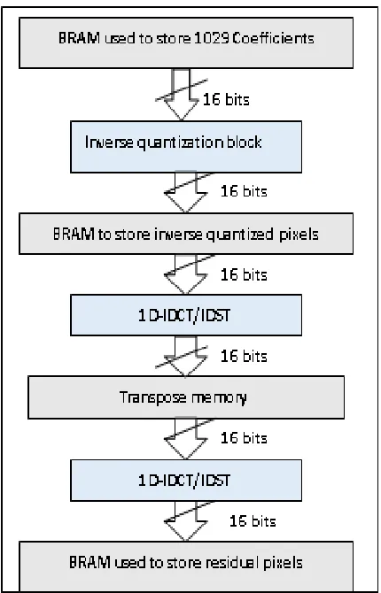
IQ/IT algorithm for HEVC decoder on the Xilinx ZC702 based platform. However, the IQ/IT C code is based on the HEVC reference software decoder (HM10.0) and is given as input to the Xilinx Vivado HLS 2015.2 tool in order to generate the IQ/IT hardware architecture. This code supports all TU sizes (4×4 to 32×32) for IQ/IT algorithm. As shown in Fig. 3, it contains 1029 coefficients as input including 1024 quantized coefficients and 5 parameters (TU size, IDCT/IDST mode decision, dequantized parameters and block stride). But in the output, one vector is obtained corresponding to the residual block.
Fig 4. IQ/IT hardware architecture generated by Vivado HLS
The FPGA resources and number of clock cycles of the VHDL codes generated by the vivado HLS 2015.2 for the no optimized and optimized IQ/IT architecture with all TU sizes (from 4×4 to 32×32 pixels) are depicted in Fig. 5 and Fig. 6, respectively. However, from Fig. 5, we can conclude that the FPGA resources are increased by about 2% compared to the implementation without any optimizations. But, from Fig. 6, we can see that the optimized architecture brings a decrease of about 76% in total clock cycles.
To compare our HLS solution with the previous works, only the 2D-IDCT/IDST algorithm is designed with the Xilinx HLS tool by applying the same directives (loop unrolling, pipelining, allocation and resource) which are used for the IQ/IT design. However, as shown in Fig. 7, we can conclude that the LUTs number of our proposed 2D-IDCT/IDST hardware architecture are decreased by approximately 56% with only a slight increase of 9% in the number of clock cycles compared to [16].
4 SW/HW
IMPLEMENTATION
RESULTS
OF
IQ/IT ARCHITECTURE
1927
the SW/HW implementation of the IQ/IT architecture on the Zynq ZC702 FPGA platform. The HW blocks are designed using the Vivado HLS which offer the possibility to connect the hardware IP to an AXI stream interface. This interface is specially designed for maximum bandwidth access to the on-chip memory and DDR memory. This transfer mode supports unlimited data burst sizes and provides point-to-point streaming data without using any addresses. In this case, the Xilinx vivado 2015.2 Design Suit tool is used to implement an ARM Cortex-A9 processor connected to the IQ/IT hardware core through an AXI DMA (Direct Memory Access). Subsequently, after achieving synthesis and implementation tasks, the bitstream file is loaded into FPGA. The SW/HW implementation of our design in the XC7Z020 FPGA shows that it requires 25364 (48%) LUTs, 16 (11%) RAM blocks and 44 (20%) DSP blocks. On the other hand, for the SW part, the IQ/IT block is Integrated as HW part in the HEVC test model (HM10.0) decoder [20] using the Tool Development Kit (SDK). After that, the C code of HEVC decoder is compiled and the executable file (.elf) is generated for a standalone environment on the ARM Cortex-A9 processor.
5 PERFORMANCE
EVALUATION
OF
HEVC
DECODER
To analyze the performance of HEVC decoder in terms of power consumption, frame rate and video quality different Bitstream files are used as input for the Zynq ZC702 FPGA platform in order to obtain the reconstructed video frame as output. These Bitstream are decoded using classes A, B, C and D video sequences with QP values equal to 22, 27, 32 and 37.
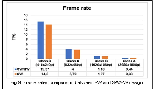
Fig. 9 depicts the comparison of the frame rates (FPS: Frame Per Second) between SW and SW/HW design for each video classes. Hence, we can see that the SW/HW design can
decode 15fps@240p in best case which presents an improvement of about 8% relative to SW implementation. It is obviously that the real time constraint is not established for the SW/HW implementation. In fact, the SW/HW design is influenced by the bus interface frequency and hardware part which are equal to 100 MHz. But, Fig. 10 presents the impact of the proposed implementations on power consumption. Indeed, from this figure, we can conclude that the SW/HW design present a decrease in power consumption about 74% compared to SW solution which runs at 700 MHz.
To objectively evaluate of the reconstructed video frame by SW/HW decoder HEVC, the average peak signal to noise ratio (PSNR) is used as a distortion measure. The PSNR makes comparison between original and resulted images, which is defined as follows:
=
−
=
Mn
o
nr
nM
PSNR
1 2
)
(
255
1
log
10
(2)Where M is the number of samples and
o
n andr
n are the amplitudes of the original and reconstructed pictures, respectively.Fig 11. (a) Original, (b) Reconstructed from SW and (c)
Reconstructed from SW/HW of the second frame of the test video sequences.
metric. Considering the above findings, we can conclude that the SW/HW design is the best method which can be more productive in term of the frame rate and the power consumption with same video quality compared to the SW solution. Therefore, the choice converges into SW/HW solution which permits a compromise between the HW performance and the SW flexibility.
6 CONCLUSION
In this work, an optimized hardware architecture based on the HLS approach for the HEVC IQ/IT algorithm supporting all sizes of TUs (4×4, 8×8, 16×16 and 32×32) is proposed. This efficient architecture is integrated in a SW/HW context for verification, where the SW part of HEVC decoder is implemented on the embedded ARM Cortex-A9 processor and the standalone IP of the IQ/IT architecture is implemented on the Xilinx XC7Z020 FPGA. Experimental results record a gain of about 8% and 74% in frame rate and power consumption respectively for the SW/HW solution compared to SW. Therefore, using HLS can reduce the FPGA development time significantly.
7 REFERENCES
[1] V. Sze, M. Budagavi, and G. J. Sullivan, High Efficiency Video Coding: Algorithms and Architectures. New York, NY, USA: Springer, 2014. [2] High E_ciency Video Coding, ITU-T Rec. H.265 and
ISO/IEC 23008-2 (HEVC), ITU-T and ISO/IEC, Apr. 2013
[3] E. Richardson, “The H.264 Advanced Video Compression Standard”, 2nd ed. West Sussex, U.K.: Wiley, 2011.
[4] M. Tikekar, C. T. Huang, C. Juvekar, V. Sze, and A. P. Chandrakasan, , “A 249-Mpixel/s HEVC Video-Decoder Chip for 4K Ultra-HD Applica-tions”, IEEE Journal of Solid-State Circuits, vol. 49, no. 1, pp. 61-72, Jan. 2014.
[5] Boudabous, A. Ben Atitallah, L. Khriji, N. Masmoudi, P. Kadionik “Efficient FPGA implementation of vector directional distance filters based on HW/SW environment validation”, Elsevier, International Journal of Electronics and Communications, VOL. 65, Issue 3, pp 250-257, March 2011.
[6] Ben Atitallah, P. Kadionik, F. Ghozzi, P. Nouel, N. Masmoudi, H. Levi “An FPGA Implementation of HW/SW Codesign Architecture for H.263 Video Coding”, Elsevier, International Journal of Electronics and Communications, Vol. 61, Issue 9, pp 605-620, October 2007. M. Kammoun and A. Ben Atitallah. “Fpga-based implementation of intra prediction module for hevc decoder”, International Journal of Recent Technology and Engineering, vol 2:pp 6130– 6137, 2019.
[7] M. Kammoun, A. Ben Atitallah, R. Ben Atitallah, N. Masmoudi “Design exploration of efficient implementation on SoC heterogeneous platform: HEVC intra prediction application”, Wiley & Sons, International Journal of Circuit Theory and Applications, Vol. 45, Issue 12, pp 2243-2259, December 2017.
[8] Xilinx, “Vivado Design Suit Tutorial: High-Level Synthesis”,https://www.xilinx.com/support/documentat ion/sw_manuals
Intel, “OpenCL Intel Corporation,”
[9] https://www.intel.com/content/www/us/en/tool/progra mmable/sdk-for-opencl/overview.html (2019).
[10]J. Villarreal, A. Park, W. Najjar and R. Halstead, “Designing Modular Hardware Accelerators in C with ROCCC 2.0”, IEEE FCCM’10, Charlotte, NC, USA, May 2010.
[11]M. Kthiri, B. Le Gal, P. Kadionik, A. Ben Atitallah, “A very high throughput deblocking filter for H.264/AVC”, Springer, Journal of Signal Processing Systems, Vol. 73, Issue 2, pp 189-199, November 2013.
[12]Ben Atitallah, P. Kadionik, F. Ghozzi, P. Nouel, N. Masmoudi, Ph. Marchegay “Optimization and implementation on FPGA of the DCT/IDCT algorithm”, IEEE ICASSP '06, Toulouse, France, 14-19 May 2006.
[13]K. Gruttner et al., “SystemC based modelling, seamless refinement, and synthesis of a JPEG 2000 decoder,” in Des., Autom. and Test Europe, Munich, Germany (2008).
[14]X. Liu et al., “High level synthesis of complex applications: an H.264 video decoder,” in Proc. ACM/SIGDA Int. Symp. Field-Programmable Gate Arrays, Monterey, California, pp. 224–233 (2016). [15]E. Kalali and I. Hamzaoglu, “FPGA implementations
of HEVC inverse DCT using high-level synthesis”, in Int. Conf. Des. and Archit. Signal and Image Process. (DASIP), Krakow, Poland (2015).
[16]R Gweon, Y. Lee, “N-Level Quantization in HEVC”, IEEE international Symposium on Broadband Multimedia Systems and Broadcasting, Seoul, South Korea, 27-29 June 2012
[17]G. J. Sullivan, J.-R. Ohm, W.-J. Han, and T. Wiegand, “Overview of the high efficiency video coding (HEVC) standard”, IEEE Trans. Circuits Syst. Video Technol., vol. 22, no. 12, pp. 1649–1668, Dec. 2012.
[18]M. Kammoun, E. Maamouri, A. Ben Atitallah, N. Masmoudi “An Optimized Hardware Architecture Of 4×4, 8×8, 16×16 And 32×32 Inverse Transform for HEVC”, IEEE ATSIP’16, Monastir, Tunisia, March 2016.