Themed Section: Science and Technology
Low Power and Area Efficient 256-bit Shift Register based on
Pulsed Latches
K.V.Janardhan1, K.Chandra Mouli2
1PG Scholar, JNTUA College of Engineering, Anantapuramu, Andhra Pradesh, India
2Lecturer, Department of ECE, JNTU College of Engineering, Anantapuramu, Andhra Pradesh, India
ABSTRACT
Shift Registers are the basic building blocks in VLSI design. Power and Area in the Shift Registers can be reduced by replacing the Flip Flops with Pulsed Latches. Delay has less importance in this method as we are not introducing any circuit elements either in between the flip flops or in between the latches. While shifting the data there arises a timing problem between the pulsed latches. To eliminate the timing problem between the latches multiple non-overlapped delayed pulsed clock signals are introduced instead of a single pulsed clock. By grouping the latches to several sub-shifter registers and adding the temporary storage latch per each sub-shifter register involves in the design to make n-bit Shift Register. The proposed Shift Register at VDD =1.8volts and
100MHZ clock frequency saves 37% area and 44% of power compared to conventional Shift Register with Flip Flops.
Keywords : Flip Flop, Pulsed clock signal, Pulsed Latch, Shift Register
I.
INTRODUCTION
Shift Registers are generally used in many applications such as digital Filters, communication receivers and Image processing ICs. As the size of the image data continueously increases the word length of the shift register which we need to process will also increases.For example a 16 mega pixel cmos image sensor uses 45k-bit shift register and a 10-bit 208 channel output LCD column driver ICs uses 2k-bit shift registers. As the word length of the shift register increases the power consumption and area of the shift register increases such as degrades the performance factors.
Generally an N-bit shift register uses n-number of data flip flops. As we are not introducing any circuit delays in between the Master-Slave flip flops the performance factor (delay) won’t effects the architecture design more. To reduce the area and
power a smallest flip flop in its design should be needed. Most recently Pulsed Latches have replaced by the flip flops to achieve better performance as the pulsed latches are much smaller in their design than that of normal flip flops.
While dealing with Master-slave flip flop it requires 2 latches and inverted clock to obey the master-slave condition to store data. But a pulsed latch uses a single latch. So we can reduce the area upto 50% and by using pulsed clock signal power consumption also reduced.
(a) (b)
The proposed shift register solves the timing problem between the latches using multiple non-overlapped delayed pulsed clock signals. The architecture design and sub shifter register patterns are discussed in various sections.
II.
ARCHITECTURE DESIGN
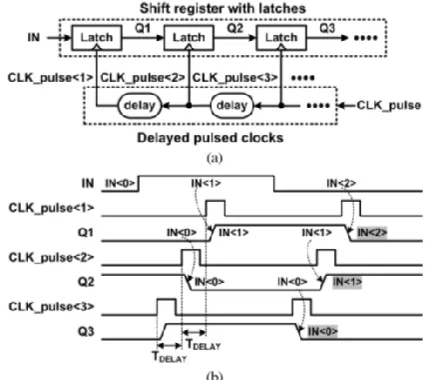
A Master-Slave flip flop with two latches can be replaced by a pulsed latch with pulsed clock signal applied externally. A pulse generator circuit will converts the applied clock into pulsed clock signal to reduce the power in the designing. Similarly all the pulsed latches share the applied pulsed clock signal so that area also reduced. Generally a pulsed latch can’t be used in shift registers due to timing problem . Timing problem in the shift registers is discussed as follows.
Figure 2.(a) pulsed latches with pulsed clock signal,(b)Timing problem in shift register
Figure 2.a consists of several latches triggered by pulsed clock signal. All latches gets activated while clock pulse signal in at high(logic-1). The output waveform Q1 for an applied input is error free as the input is constant throughout the width of pulsed clock. As Q1 is input to the next latch as well as it is not constant throughout the width of clock pulse, output Q2 suffers from timing problem. It depends on the rise and fall times of the logic levels. Here the timing
a. Solutions to Timing Problem
Adding a delay to the shift register will solve the timing problem. This delay can be introduced in two ways to eliminate the timing problem as follows
Figure 3.(a) latches with delay,(b)delayed output logics
In the Figure 3.(a) delay is introduced in between the latches, due to this delay the output waveform Q1 reaches the next latch after the pulsed clock so that timing problem can be eliminated. One more method to eliminate timing problem is discussed as follows.
Figure 4.(a) latches with multiple non-overlapped delayed pulsed clock,(b)propagation in output
waveforms.
constant input signals throughout the pulsed clock width. But both these methods cause performance degradation i.e. area and power increases by the additional delay circuits. So to reduce area and power we go through the designing of sub shifter registers based on even integers to reduce delay elements in the design.
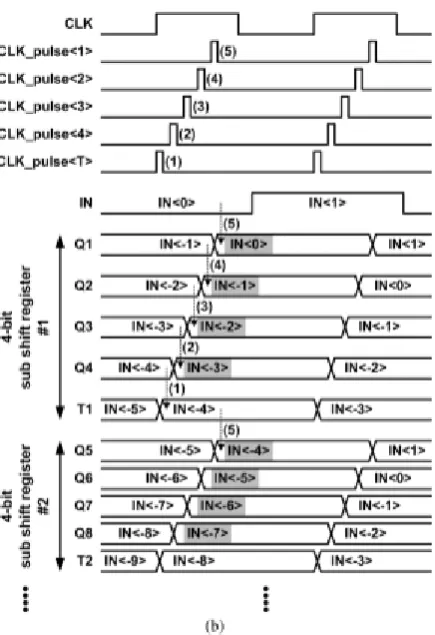
b. Designing Sub Shifter Register
In order to reduce area and power in the Shift Registers we divide the N-bit shift register into M K-bit sub shifter registers. By making these sub shifter registers we can decrease the number of delayed pulsed clock signals. Generally K-bit sub shifter register contains K+1 latches and K+1 multiple non-overlapped delayed pulse clock signals. In this paper we proposed 256-bit shift registers with K=4 so that we have 64 bit sub shift registers in the design. A 4-bit sub shifter register has 5 latches and 5 multiple non-overlapped delayed pulse clock signals. In the first sub shifter register 4 latches store the 4-bit data i.e (Q1-Q4) and fifth latch acts as temporary storage latch to update the second sub shifter register i.e which starts from Q5. The sequence of pulsed clock signals is in opposite order of latches in sub shifter register because T1 should be ready to store and forward data from Q4 to Q5. All the latches updated with binary logics from their previous latches except Q1 as it is updated by applied input logic. This process of data propagation will continued till the last latch is updated. The sub shifter register design is as follows with K=4.
Figure 5.(a) 4-bit sub shifter register schematic design
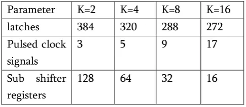
By making the sub shifter register design we can reduce the number of pulsed clock signals but it increase the additional temporary storage latches. An N-bit shift register requires [N+(N/K)] latches and K+1 pulsed clock signals totally. Where N/K represents the number of sub shifter registers. For a 256-bit shift register different parameters are as follows.
Table: 1. 256-bit SR with different K values Parameter K=2 K=4 K=8 K=16
latches 384 320 288 272
Pulsed clock signals
3 5 9 17
Sub shifter registers
Figure 5.(b) data shifting in sub shifter registers
In the conventional delayed pulsed clock signals (Figure 4.a) pulse width of clock signals should be larger than the summation of trise and tfall of all
inverters to maintain shape of the clock pulse. However in multiple non-overlapped delayed pulsed clock signals the width of the clock pulse can be shorter than the summation of trise and tfall of inverters
because each clock pulse is generated from AND gate and two delayed signals. Thus clock pulse generator is suitable for short pulsed clock signals.
C. Predetermined conditions in CPG
While designing the Clock Pulse Generator circuit maximum number of K limits the target clock frequency. The minimum clock cycle time is given by Tclk-min=Tcp+(K*Tdelay)+Tcq. Where Tcp is the delay from
rising edge of main clock to rising edge of the first
that target frequency will decreases. So that K value should select under maximum clock frequency of targeted applications.
Figure 6.(a)Delayed pulsed clock generator
Figure 6.(b) Minimum clock cycle time for SR
As introducing the delay elements in the pulsed clock generator, different pulse clocks will arrives at different time in each sub shifter register due to pulse skew. As increase in the wire distance pulse skew also increases. The clock pulse intervals are larger than pulse skew will cancel out the skew difference and no timing problem occurs because the clock pulses connecting two different sub shifter registers have enough pulse intervals. For long shift registers a short pulses won’t suite because as wire length increases pulse shape gets degraded by wire capacitance and resistance. To overcome this problem we connect the clock buffers to boost up the pulses with less wire delay. However this increases area so that K value should be optimum.
considered under implement design. Design unit has 600 bonded IOBs and nearly 2k logic cells to be implemented in chip with 35*35mm size. Vcc for chip
can be of 1.8v in proposed design. The synthesis results are as follows for design.
IV.
SYNTHESIS RESULTS
We have developed Verilog code for Shift Registers in both Flip Flop and Pulsed Latch models. The waveforms for the design can be observed in Integrated Synthesis Environment(ISE) and Modelsim Altera will supports the Synthesize the design.
Figure 7.(a)Shift Register with Flip Flops(256-bit)
Figure 7(b). Technology Schematic for 16-bit design
The technology schematic will provides the register based design i.e. encoders, multiplexers, buffers, Flip Flops which will make the LUTs fully utilized. In the
other hand 256-bit Shift Register with pulsed Latches Design is consists of only bonded IOBs in its schematic thus the area of utilization is less compared to Flip Flop methodology. The wave forms for the Pulsed Latch design can be given by as follows.
Figure 8.(a) Shift Register with Pulsed Latches method
Figure 8.(b) RTL Schematic for 16-bit SR design
in existing method design area included utilization of 24% of LUT-FF pairs and 3% of global buffers besides 43% of bonded IOBs. The Area utilization can be given by as follows.
Figure 9.(a) Area utilization in proposed method
Figure 9.(b) Area utilization in existing method
For different bit designs the area minimization table for proposed technology can be given by as follows.
Table 2 Shift
Registe r
Bonded IOBs(%)
Fully used LUT-FFpairs( %)
Global buffers( %)
Area minimi zed(%)
FF Latch
FF Latch
FF Latch
16-bit 3 8 17 0 3 0 34.61 32-bit 5 17 20 0 3 0 34.00 128-bit 21 21 23 0 3 0 33.50 256-bit 43 42 24 0 3 0 33.41
Figure 10.(b)Area on FPGA for N-bit Shift Register
Similarly power for both methodologies were calculated using Xpower Analyzer in XILINX 13.2 with clock frequency of 100MHZ for implemented FPGA and it can be operated at Fmax of 840MHZ for
clock. The power for N-bit shift registers can be tabled as follows.
Figure 11.(a) Power leakage in proposed shift register
Shift Register
Power leakage in design(mW)
FF Latch
Power saving (%)
16-bit 207 169 18.35
32-bit 266 212 20.30
128-bit 475 373 21.26
256-bit 682 529 22.43
Figure 11.(b) Power minimization in proposed method
0 20 40 60 80 100 120
16-bit 32-bit 128-bit 256-bit
Flip Flop
Figure 11.(c) Power leakage in N-bit Shift Registers
V.
CONCLUSION
In this paper we proposed Shift Register design with pulsed latches to reduce power and area compared to existing flip-flop based design. Timing problem in latch based design is solved by introducing multiple non-overlapped delayed pulsed clock signal instead of single pulsed clock. Most recently a latch is replaced by flip-flop to save area and power as it is much smaller in size so that power also reduces. With the proposed technology we reduced the power and area in 256-bit shift register upto 28% and 35% in average respectively. As we are replacing the flip-flops with pulsed latches it can be introduced in many applications like standard cells, SRAM(as it is volatile) we can store and fetch 1-bit data based on bit-line condition. Similarly we can deal with microprocessors to minimize stacked transistors as it use less dynamic power.
VI.
REFERENCES
[1]. H. Yamasaki and T. Shibata, "A real-time image feature-extraction and vector-generation vlsi employing arrayed-shift-register architecture," IEEE J. Solid-State Circuits, vol. 42, no. 9, pp. 2046–2053, Sep. 2007.
[2]. H.-S. Kim, J.-H.Yang, S.-H.Park, S.-T.Ryu, and G.-H. Cho, "A 10-bit column-driver IC with parasitic insensitive iterative charge-sharing based capacito rstring interpolation for mobile
active-matrix LCDs," IEEE J. Solid-State Circuits, vol. 49, no. 3, pp. 766–782, Mar. 2014. [3]. P.Reyes,P.Reviriego,J.A.Maestro,andO.Ruano,"
Newprotection techniques against SEUs for moving average filters in a radiation environment," IEEE Trans. Nucl.Sci.,vol.54,no.4,pp.957–964,Aug. 2007. 4M. Hatamian et al., "Design considerations for gigabit ethernet 1000 base-T twisted pairtransceivers," Proc. IEEE Custom Integr.Circuits Conf., pp. 335–342, 1998. [4]. S.-H. W. Chiang and S. Kleinfelder, "Scaling and
design of a 16-megapixel CMOS image sensor for electron microscopy," in Proc. IEEENucl. Sci. Symp. Conf. Record (NSS/MIC), 2009, pp. 1249–1256.
[5]. S. Heo, R. Krashinsky, and K. Asanovic, "Activitysensitive flip-flop and latch selection for reduced energy," IEEE Trans. Very Large ScaleIntegr. (VLSI) Syst., vol. 15, no. 9, pp. 1060–1064, Sep. 2007.
[6]. S. Naffziger and G. Hammond, "The implementation of the next generation 64 bit anium microprocessor,"inIEEEInt.Solid-StateCircuits
Conf.(ISSCC)Dig.Tech.Papers,Feb.2002,pp.276– 504. 8H. Partovi etal., "Flow-through latch and edge-triggered flip-flop hybrid elements,"IEEEInt.Solid-State Circuits Conf.(ISSCC)Dig.Tech. Papers, pp. 138–139, Feb. 1996.
[7]. J.Montanaroetal.,"A160-MHz,32-b,0.5-WCMOS RISC microprocessor," IEEE J. Solid-State Circuits, vol. 31, no. 11, pp. 1703–1714, Nov. 1996.
[8]. S. Nomura et al., "A 9.7 mW AAC-decoding, 620 mW H.264 720p 60fps decoding, 8-core media processor with embedded forward body-biasing and power-gating circuit in 65 nm CMOS technology," in IEEE Int. Solid-State Circuits Conf. (ISSCC) Dig. Tech. Papers, Feb. 2008, pp. 262–264. 0 200 400 600 800 1000 1200 1400
16-bit 32-bit 128-bit 256-bit
Flip Flop
11Y.Uedaetal.,"6.33mWMPEGaudiodecodingon a multimediaprocessor,"inIEEEInt.Solid-StateCircuitsConf.(ISSCC)Dig.Tech.Papers, Feb. 2006, pp. 1636–1637.
[9]. B.-S. Kong, S.-S. Kim, and Y.-H. Jun, "Conditional-capture flip-flop for statistical power reduction," IEEE J. Solid-State Circuits, vol. 36, pp. 1263–1271, Aug. 2001
About Authors:
Mr. K.V. Janardhan completed B.Tech in ECE from Santhiram Engineering College (SREC) Nandyal in 2014. Now he is pursuing M.Tech degree in JNTUA college of engineering Anantapuramu. His areas of interests are VLSI Design and Digital Electronics.