Abstract— The outstanding mechanical properties of silicon on
insulator (SOI) wafers make it popular for high-performance MEMS sensors such as accelerometers. Other advantages include the fabrication of structures at a very high aspect ratio using deep reactive ion etching, facilitation of the integration of MEMS and integrated circuit on the same wafer, exhibition of superior electrical performances by effective electrical isolation between two silicon layers, and reduction of process complexity and costs using SiO2 as an etch stop. The current work demonstrates the design and simulation of a capacitive Z-axis accelerometer based on the SOI-MEMS technology.
Index Term— Capacitive accelerometer, silicon on insulator, MEMS, silicon on insulator, simulation
I. INTRODUCTION
Recently, there has been a gradual increase in the fabrication of MEMS accelerometers on SOI wafer [1]–[6]. This is due to various advantages of SOI wafer, namely, its superior material properties, capability to reduce process complexity and cost, and feasibility of MEMS and IC integration [6], [7]. Several SOI-MEMS accelerometers have been successfully designed and fabricated. However, few of them actualize a Z-axis accelerometer with differential capacitive sensing [2]. Thus, the demand for high-performance SOI-MEMS accelerometers (high sensitivity, high resolution, low noise, etc.) for various applications remains.
The majority of commercial MEMS accelerometers are presently used as capacitive-type sensing mechanisms due to their high sensitivity, low noise, low temperature sensitivity, and low power dissipation characteristics [8]. The design and simulation of an SOI-MEMS capacitive Z-axis accelerometer using the architect module in CoventorWare2010 is presented in this work. The main goals of this study are to achieve high
sensitivity and wide bandwidth in an SOI-MEMS capacitive z-axis accelerometer.
II. MATERIALANDMETHODS
The capacitive accelerometer converts the displacement signal into an electrical signal. Figure 1 shows the layout of an SOI-MEMS capacitive Z-axis accelerometer. The proof mass is suspended by four compliant beams anchored to a fixed frame. The physical parameters of the beam in this device, such as the shape, geometry, and materials used, need to be carefully considered because they will influence the stiffness of the beam. Lowering the spring stiffness means reducing the natural frequency of the accelerometer, thereby reducing the operating bandwidth [9], [10]. To achieve the desired performance, it is necessary to ensure that the proof mass moves smoothly and the cross-axis sensitivity is low. To minimize the off axis deflection, the L-beam is designed and adjusted to be at the center of the device mass, so that when the force is acting on the device mass, the motion of the device mass is corresponding to the centre of gravity.
The capacitive accelerometer converts the displacement signal into an electrical signal. Figure 1 shows the layout of SOI-MEMS capacitive z-axis accelerometer. The proof mass is suspended by four compliant beams anchored to a fixed frame. The beam shape physical parameters such as the shape, geometry and material used in this device need to be carefully considered because these properties will influence the stiffness of the beam. Lowering spring stiffness means reducing the natural frequency of the accelerometer. Consequently, the operating bandwidth will also be reduced [9]. In addition, it will lead the beam at handle layer [10]. In order to achieve the desired performance, it is important to ensure that the proof mass is moving without stick and the cross axis sensitivity is lowered. These problems were prevented by designing L-beam to be at centre of mass gravity of the beam correspond to the center of mass, so that the off axis deflection can be minimized.
Design and Simulation of SOI-MEMS Z-axis
Capacitive Accelerometer
O. Sidek, M. Afif and M.A. Miskam
Financial support from the Universiti Sains Malaysia Short Term Grant, 3004/PCEDEC/60310013 is gratefully acknowledged. O. Sidek is with the Collaborative Microelectronic Design Excellence Center, Universiti Sains Malaysia, 14300 Nibong Tebal, Pulau Pinang
Malaysia ([email protected]).
M. Afif is with the is with the Collaborative Microelectronic Design Excellence Center, Universiti Sains Malaysia, 14300 Nibong Tebal, Pulau
Pinang Malaysia (Phone: +6045995856; Fax: +6045941025; [email protected]).
Fig. 1. Layout of the SOI-MEMS capacitive z-axis accelerometer
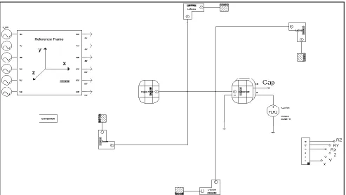
The physical dimensions employed in the simulation are listed in Table I. The architect model is shown in Fig. 2. The steps of the fabrication process are illustrated in Fig. 3.
TABLE I PHYSICAL DIMENSIONS
Properties Variable Name Value (µm)
Plate Width WP 1000
Plate Length LP 1000
Beam length:
Beam A LBa 300
Beam B LBb 380
Beam width WB 50
Hole Width Wh 50
Hole Length Lh 50
Device Thickness 2.5
Oxide Thickness 1
Handle Thickness 625
Aluminum Thickness 0.5
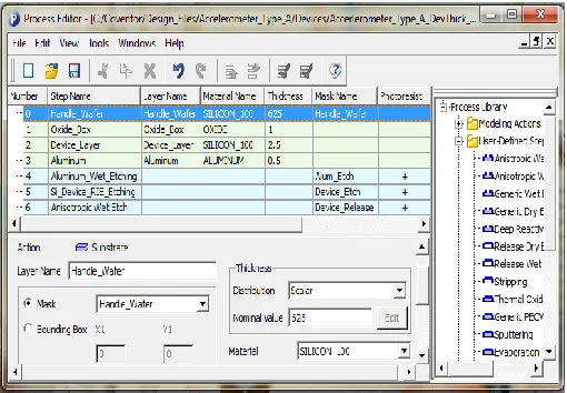
Fig. 2. Steps for the fabrication process of a SOI-MEMS capacitive z-axis accelerometer
The SOI wafer used was produced using the SIMOX method [11]. The wafer consists of three layers: the handle
layer located in the bottom, the silicon dioxide (SiO2) layer in
the middle, and the device layer at the top (Fig. 4). The middle layer separates the device layer and handle layer, and acts as a
gap when the SiO2 layer is etched in order to release the
structure. The 1 µ gap between the device and handle layers has been controlled and optimized, ensuring that the gap is uniform when the SOI wafer is produced in the manufacturing stage. Thus, the optimized gap can be easily archived without compromising the masking design, which can be very costly. The process of fabrication can be simplified as well. The device layer at the top comprises beams, mass, and a plate that will couple with the handle layer at the bottom. These two layers then function as a sensor capacitance. Holes in the device plate have two purposes: (1) to ease the fabrication
process when releasing the structure, enabling the SiO2 layer in
the middle layer to be conveniently etched through the holes, and (2) to repress the squeezed-film effect so that the accelerometer has a good frequency response.
Fig. 3. Schematic of the structure in the Architect module of CoventorWare2010.
Fig. 4. 3D model
The capacitive sensitivity of the z-axis accelerometer is given by Equation (1).
o
o C
C x
S
a d a
(1)
where C is the capacitance, a is the acceleration, d is the air
gap, and x is the displacement of the proof mass.
III. RESULTSANDDISCUSSION
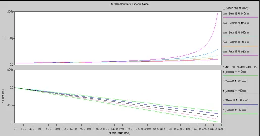
In this study, the length of multiple beams was varied to obtain the optimum and linear capacitance increment without lowering the sensitivity, and to easily develop the readout
circuit. The effect of LbB length is shown in Figure 6 and the
physical parameter is listed in Table 1. From the results, the
LbB with a length of 380µm was choosing. Figure 5 shows the
result of displacement and capacitance during a steady state condition at Time 0. The initial capacitance of the accelerometer was found to be approximately 7.325 pf, and the displacement at z, x, and y axis was very small. The length of the beam can greatly influence the total sensitivity and the performance of the device (Fig. 6). The performance required in terms of mechanical sensitivity can be raised to the desired performance by manipulating the length of the beam. The effort to increase the sensitivity by increasing the beam length will result in a complex readout circuitry. In addition, it will reduce the operating range of the accelerometer.
The resonant frequency for the z-axis is approximately 4.1 kHz (voltage pulse is set to 1 volt), whereas it remains the same in the x and y-axis, as shown in Fig. 7. In this simulation, the device is given an input from 0 until 50 g (1 g is equal to
9.98 ms-1), as shown in Fig. 6. The output will then be in terms
Table 2 below exhibits the summary of results from the simulation.
TABLE 2
SUMMARY OF THE RESULT
Parameter Value
Static Capacitance (pF) 7.325
Natural frequency (kHz):
Z 4.1
X 4.1
Y 4.1
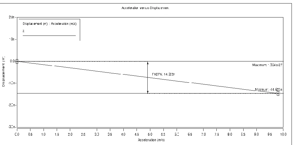
Sensitivity per 1 g acceleration:
Displacement 14.622 nm/g
Capacitance 103.55 fF/g
Fig. 5. DC operating point analysis.
Fig. 7. Frequency response for the Z-axis accelerometer
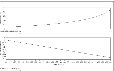
(a)Sensitivity per 1g acceleration (Acceleration vs. Capacitance)
(b)Sensitivity per 1g acceleration (Acceleration vs. Displacement)
Fig. 9. Sensitivity analysis result for accelerometer for 1 g
IV. CONCLUSION
A design and simulation of SOI-MEMS capacitive z-axis accelerometer is examined in this paper. The designed accelerometer was found to be capable of actuating up to 50 g acceleration with sensitivity of approximately 103.551 fF. The beam length has significant influence on the sensitivity and operating bandwidth of the accelerometer. Therefore, the
required performance and manufacturing capability can be achieved by compromising the structural design and fabrication process.
REFERENCES
[2] Chia-Pao Hsu, Ming-Chuen Yip and Weileun Fang, “Implementation of a gap-closing differential capacitive sensing Z-axis accelerometer on an SOI wafer,” J. Micromech. Microeng, vol. 19, 2009, pp. 1-7.
[3] Aziz, A.A., Sharaf, A.-H., Serry, M. and Sedky, S., “Novel architecture for inertial grade SOI MEMS inertial sensors,” Proceedings of IEEE International SOI Conference, 2009, pp. 1-2.
[4] William D Sawyer, Mert S Prince and Giles J Brown, “SOI bonded wafer process for high precision MEMS inertial sensors,” J. Micromech. Microeng., vol. 15, 2005, pp. 1588–1593.
[5] Amini, B.V., Abdolvand, R. and Ayazi, F., “Sub-micro-gravity capacitive SOI microaccelerometers,” Prooceedings of 13th International Conference on Solid-State Sensors, Actuators and Microsystems, 2005, pp. 515 – 518.
[6] B. Diem, P. Rey, S. Renard, S. Viollet Bosson, H. Bono, F. Michel, M.T. Delaye, G. Delapierre, “SOI 'SIMOX'; from bulk to surface micromachining, a new age for silicon sensors and actuators,” Sensors and Actuators A: Physical, vol. 46, Issues 1-3, 1995, pp. 8-16. [7] Kalyan Kumar Mistry, K. B. M. Swamy, Siddhartha Sen, “Design of an
SOI-MEMS high resolution capacitive type single axis accelerometer,”
Microsyst Technol., 2010.
[8] Manut, A., Syono, M.I., “Effects of Mechanical Geometries on Resonance Sensitivity of MEMS Out-of-Plane Accelerometer,” Proc. of IEEE Int. Conf. on Semiconductor Electronics, 2006, pp. 25-28. [9] Chih-ming Sun, ChuanWei Wang, Weileun Fang, "On the sensitivity
improvement of CMOS capacitive accelerometer," Sensors and Actuators A: Physical, vol. 141, 2008, pp. 347-352.
[10] Huikai Xie, Gary K. Fedder, Robert E. Sulouff, “Accelerometers,”
Comprehensive Microsystems, 2008, Chapter 2.05, pp. 135-180. [11] T. Tsuchiya and H. Funabashi, "A z-axis differential capacitive SOI
accelerometer with vertical comb electrodes," Sensors and Actuators A: Physical, vol. 116, pp. 378-383, 2004.