402 |
P a g e
A REVIEW PAPER ON POWER REDUCTION
TECHNIQUES FOR FULL ADDER
Trapti Mittal
1, Uma Sharma
2 1,2Department of ECE, Ajay Kumar Garg Engineering College Ghaziabad, (India)
ABSTRACT
Full adder is a basic building for a wide range of the applications such as ALU and multipliers; it is used as a key
element for the critical path in the microprocessors, so it should be faster and shows less power consumption.
Silicon on Insulator is a modern day technology after the bulk CMOS, it shows effective reduction in the leakage
current, delay an power consumption. Adder performance can be improved by efficiently implementing, the carry
propagation chain. This can be addressed by either improving the structure of the 1-bit full adder which is one of the
basic cells in adders such as the ripple carry adder or carry select adder or carry skip adder.
Keywords - Delay, Full Adder, Power Consumption, SOI, ULPFA.
I INTRODUCTION
With the advancement of VLSI technology, many computing intensive applications such as multimedia processing,
digital communication can now be realized in hardware to either speed up the operation or reduce the power/energy
consumption. Transistor count is one of the major concerns, as it also leads to a reduction in delay for the circuits.
Two other important yet often conflicting design criteria are power consumption and speed. A better metric would
be the power delay product or energy consumption per operation to indicate the optimal design tradeoffs.
Although dynamic power is continuously being reduced with technology scaling, static leakage power tends to
increase and is expected to become a large contributor to total power in a few technology generations [1].
There are three major components of power dissipation in complementary metal–oxide–semiconductor (CMOS)
circuits.
1) Switching Power: Power consumed by the circuit node capacitances during transistor switching.
2) Short Circuit Power: Power consumed because of the current flowing from power supply to ground during
transistor switching.
3) Static Power: Due to leakage and static currents.
In the Bulk CMOS technology, it shows the more parasitic capacitances, latch up problem and leakage current
problem which can be overcome in the SOI technology. SOI technology was extracted from bulk technology by
incorporating oxide layer over the silicon substrate, 50% of the problem was solved such as leakage currents,
403 |
P a g e
architectures allow optimum electrical properties to be obtained for low power and high performance circuits. InSOI an interesting observation is that the body terminal is either tied to gate or left free for floating called as
―floating body as when the floating body is considered it has some important features in reducing power
consumption and improving the device efficiency.
In the SOI technology, the structure of the conventional CMOS full adder design shows the effective reduction then
in the bulk CMOS technology. There are various designs have been introduced for the full adder realization, using
the various XOR-XNOR realizations or based on their logic realizations.
Fulladders realized using pass transistor network provides an efficient way for the power and delay reduction as
they use the minimum number of transistors.
A pass transistor is an nMOS (pMOS) transistor with the signal input fed to the source and the signal output taken
from drain. Pass network is an interconnection of a number of pass transistors to achieve a particular switching
function. The propagation of the signal through the transistor is controlled by a signal applied to its gate. In the case
of an nMOS transistor, logic ‗1‘ at the gate passes the input from source to drain and logic ‗0‘ opens the source to
drain path. A pMOS transistor exhibits similar behavior with a control signal of logic level 0. A nMOS transistor
passes a strong ‗0‘, but a weak ‗1‘. A pMOS transistor passes a strong ‗l‘, but a weak ‗0‘.
To speed up a full adder design, a 4-transistors XOR-XNOR circuit is used called complementary and level
restoring carry logic (CLRCL) [1]. Another design [2] that compensates the threshold voltage drop introduces a
single 6-transistor XOR-XNOR cell for the full adder design. A 1-bit full adder is designed using 12 transistors, that
employ 6 multiplexers leads to a low voltage [3].
In [4], full adder is designed using hybrid approach, it uses pass transistor network and branch based logic shows the
reduction in delay, and another design uses the ultra low power diode (ULPD) that reduces the leakage current in the
sum part.
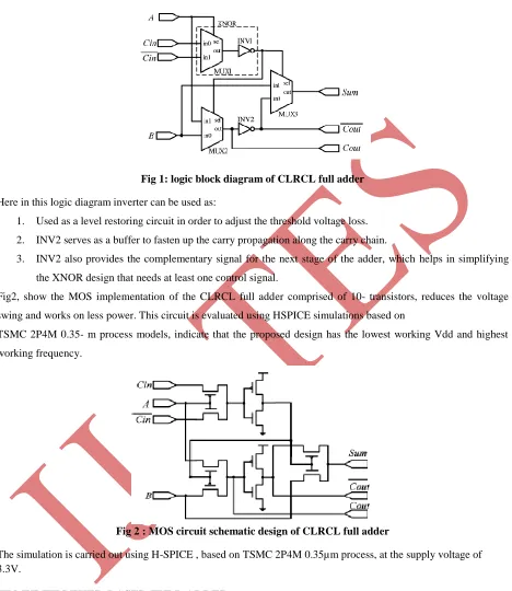
II CLRCL FULL ADDER
This paper [1] proposes a 10- transistors full adder design using the complementary and level restoring carry logic
(CLRCL). The aim is to minimize the circuit complexity and to acquire the smooth cascaded operation. This goal
can be achieved by the proper level restoring to avoid the multiple threshold voltage losses in the carry block. To
realize the full adder, the Boolean expression as follows:
Sum= (A ʘ Cin). Cout’ + (A
⊕
Cin).B
Cout= (A
⊕
Cin). B + (A ʘ Cin).A
The fig shows the block diagram of the proposed full adder consists of 2-to-1 multiplexers and inverters.
404 |
P a g e
Fig 1: logic block diagram of CLRCL full adder
Here in this logic diagram inverter can be used as:
1. Used as a level restoring circuit in order to adjust the threshold voltage loss.
2. INV2 serves as a buffer to fasten up the carry propagation along the carry chain.
3. INV2 also provides the complementary signal for the next stage of the adder, which helps in simplifying
the XNOR design that needs at least one control signal.
Fig2, show the MOS implementation of the CLRCL full adder comprised of 10- transistors, reduces the voltage
swing and works on less power. This circuit is evaluated using HSPICE simulations based on
TSMC 2P4M 0.35- m process models, indicate that the proposed design has the lowest working Vdd and highest
working frequency.
Fig 2 : MOS circuit schematic design of CLRCL full adder
The simulation is carried out using H-SPICE , based on TSMC 2P4M 0.35µm process, at the supply voltage of 3.3V.
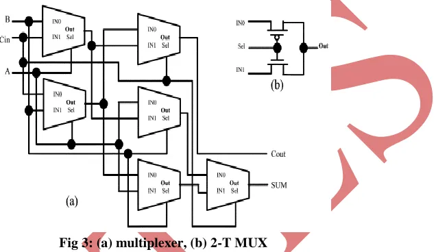
III MULTIPLEXER-BASED FULL ADDER
Here the author has proposed a 1-bit full adder cell [3] consisting of 6 multiplexers, called as MBA-12T, using 12
transistors aims on reducing the power consumption. This full adder cell design show the 26% power savings from
405 |
P a g e
it and also shows the improvement of 64% in term of speed from others. Fig.3 shows the architecture of themultiplexer based full adder design.
For any digital design, three major sources of power dissipation are: short circuit current, leakage current and logic
transition. Here the short circuit is defined as the direct current passing from supply to ground, when pMOS &
nMOS transistors are active. As the given design is not directly connected to the supply and ground, the short
current will be negligible.
Fig 3: (a) multiplexer, (b) 2-T MUX
To add to this, each multiplexer in the design is directly connected to the main input so there will not be any delay,
and show the speed improvement in the circuit. Figure 4 shows the schematic design.
Fig 4: MBA-12T full adder
The simulation is carried out in H-SPICE using TSMC 0.35µm CMOS technology at 3.3V supply and compared to
other designs at different frequencies (ranging from 10MHz to 200MHz) at different capacitive values.
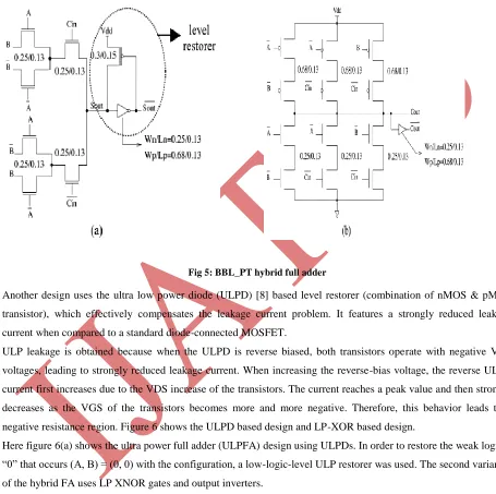
IV ULPFA: ULTRA LOW POWER FULL ADDER
The authors of the following paper [5] has introduced the full adder based on hybrid technologies, and compared to
various full adder designs and simulates the results using 0.13- m PD SOI CMOS with a supply voltage of 1.2 V.
406 |
P a g e
effective improvement in power consumption, delay that leads to power delay product (PDP) of the full adderdesign.
The BBl_PT logic design fig 5, uses the pass transistor network for the sum part and branch based logic for the carry
part, its sum part uses the level restoration concept to overcome the inherited problem of pass transistors i.e., weal
logic ‗1‘, & logic ‗0‘.
Fig 5: BBL_PT hybrid full adder
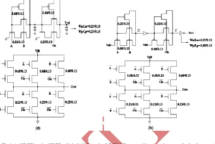
Another design uses the ultra low power diode (ULPD) [8] based level restorer (combination of nMOS & pMOS
transistor), which effectively compensates the leakage current problem. It features a strongly reduced leakage
current when compared to a standard diode-connected MOSFET.
ULP leakage is obtained because when the ULPD is reverse biased, both transistors operate with negative VGS
voltages, leading to strongly reduced leakage current. When increasing the reverse-bias voltage, the reverse ULPD
current first increases due to the VDS increase of the transistors. The current reaches a peak value and then strongly
decreases as the VGS of the transistors becomes more and more negative. Therefore, this behavior leads to a
negative resistance region. Figure 6 shows the ULPD based design and LP-XOR based design.
Here figure 6(a) shows the ultra power full adder (ULPFA) design using ULPDs. In order to restore the weak logic
―0‖ that occurs (A, B) = (0, 0) with the configuration, a low-logic-level ULP restorer was used. The second variant
407 |
P a g e
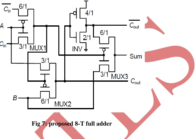
Fig 6: (a) ULPFA using ULPDs, (b) hybrid FA using LP-XNOR gates with output invertors for level restoration.V DESIGN OF A NOVEL LOW POWER 8-TRANSISTOR 1-BIT FULL ADDER CELL
The authors of this paper are proposing a novel 1-bit full adder cell, which is constructed using only 8 transistors. It
takes 3 multiplexers and an inverter that helps in reducing the power dissipation. This design also helps in reducing
the transistor count and leads to faster output. the power consumption, propagation delay and power delay produced
using the new design are analyzed and compared with those of other designs using HSPICE simulations.
The proposed full adder follows the following Boolean expression:
Sum = (A
⊕
Cin). Cout’ + (A
⊕
Cin)’. B,
Cout = (A
⊕
Cin). B + (A
⊕
Cin)’. A.
Fig 7 shows the full adder design proposed by the authors.
The entire design process can be divided into several steps as follows:
408 |
P a g e
2. The multiplexer circuit MUX2 is adopted in our proposed design to generate Cout followed by an inverter INV.The inverter has three advantages for the circuit: firstly, it speeds up the carry propagation as a buffer along the carry
chain.
Fig 7: proposed 8-T full adder
Secondly, it provides complementary signals needed for the generation of Sum. Thirdly, the inverter can improve
the output voltage swing as a level restoring circuit (Lin et al., 2007).
3. The Sum is generated by the multiplexer MUX3 passing either B or Cout according to the value of in (A⊕C)‘.
To test the performance of the proposed full adder, detailed comparisons were performed. All the schematics are
based on TSMC 180 nm technology with a 1.8 V supply voltage, and were simulated using HSPICE. In our
simulation, the power consumption of these designs was examined at different input frequencies. The frequencies
ranging from 100 t 500 MHz and the output load of 100fF. it shows the power reduction from other adder is about
7.2%- 32.8%. It can be efficiently used in other arithmetic large applications.
VI CONCLUSIONS
Here in this review paper, we have reviewed and discussed four papers which shows the advantages and
disadvantages of the full adder cells .among these paper ULPFA shows the most improvement in terms of power
consumption and delay and power delay product but due to the use of ULPD, it employs more transistor than others.
In future we need to such a full adder block so that it works smoothly in the larger applications for the arithmetic
409 |
P a g e
REFERENCES
[1] Jin-Fa Lin, Yin-Tsung Hwang, Member, IEEE, Ming-Hwa Sheu, Member, IEEE, and Cheng-Che Ho, ―A Novel
High-Speed and Energy Efficient 10-Transistor Full Adder Design‖ IEEE TRANSACTIONS ON CIRCUITS AND
SYSTEMS—I: REGULAR PAPERS, VOL. 54, NO. 5, MAY 2007.
[2] D.Radhakrishnan, ―Low-voltage low-power CMOS full adder‖ IEE PROC.-CIRCUITS DEVICES SYST., VOL.
148, NO. I , FEBUARY 2001.
[3] Yingtao Jiang, Abdulkarim Al-Sheraidah, Yuke Wang, Edwin Sha, and Jin-Gyun Chung,‖ A Novel
Multiplexer-Based Low-Power Full Adder‖ IEEE TRANSACTIONS ON CIRCUITS AND SYSTEMS—II: EXPRESS BRIEFS,
VOL. 51, NO. 7, JULY 2004.
[4] Farshad Moradi, Dag.T. Wisland, Hamid Mahmoodi, Snorre Aunet, Tuan Vu Cao, Ali Peiravi, ―Ultra Low
Power Full Adder Topologies‖, CIRCUIT AND SYSTEMS, 2009. ISACAS 2009. IEEE INTERNATIONAL
SYMPOSIUM, MAY 24, 2009.
[5] Ilham Hassoune, Denis Flandre, Senior Member, IEEE, Ian O‘Connor, Senior Member, IEEE, and Jean-Didier
Legat, Member, IEEE, ―ULPFA: A New Efficient Design of a Power-Aware Full Adder‖ IEEE TRANSACTIONS
ON CIRCUITS AND SYSTEMS—I: REGULAR PAPERS, VOL. 57, NO. 8, AUGUST 2010.
[7] Yi WEI, Ji-zhong SHEN, ―Design of a novel low power 8-transistor 1-bit full adder cell‖ Journal of Zhejiang
University-SCIENCE C (Computers & Electronics) ISSN 1869-1951 (Print); ISSN 1869-196X (Online)
www.zju.edu.cn/jzus; www.springerlink.com, 25, Jan 2011.
[8] V. Dessard, ―SOI specific analog techniques for low-noise, high-temperature or ultra-low power circuits,‖