Implementation of Dynamic Voltage Restorer
for Voltage Sag Mitigation
1.
S.DEEPA 2.Dr.S.RAJAPANDIAN
1.
Research Scholar, Sathyabama University, Chennai, India.
2.
Professor,Panimalar Engineering College, Chennai, India.
Abstract:
The dynamic voltage restorer (DVR) has become popular as a cost effective solution for the protection of sensitive loads from voltage sags and swells. In principle, it would be advantageous if the series connected inverter of a DVR could also be used to compensate for any steady state load voltage harmonics, since this would increase the Power Quality ‘value added’ benefits to the grid system. However, before this can be done, consideration must be given to the control of steady state power through the DVR, the increased losses, and the low modulation depths at which the scheme must operate to achieve acceptable harmonic compensation performance. This paper presents a selective harmonic elimination using flying capacitor connection. simulations and Experimental results are presented to verify the performance of the 8 bus DVR system
Keywords: Power quality, voltage sags, DVR, Voltage source inverter (VSC), Harmonic elimination, flying capacitor.
1. Introduction
Dynamic Voltage Restorers (DVR) are now becoming more established in industry to reduce the impact of voltage sags to sensitive loads [1-3]. However, since voltage sags generally only occur a few times each year at any particular location, a DVR system will generally spend most of its time in standby mode waiting for sag to occur. But unfortunately, it will still introduce extra impedance to the line, primarily due to the series transformer; and this impedance will (in turn) cause a voltage drop to the load and increased load voltage harmonics when non-linear loads are present [4]. In principle, it would be advantageous if the series connected inverter of the DVR could also be used to compensate for any steady state load voltage harmonics. This would increase the Power Quality ‘value added’ benefits to the system (which is the definition and driving force of Custom Power applications) with minimal extra capital cost, but of course with some increase in inverter steady state losses. The limitations in achieving this objective are steady state power flow constraints and the low modulation depths that must be used with a DVR that has a typical voltage injection capacity. Fig. 1 shows a typical DVR series-connected topology, with a short-term energy storage capability (such as a capacitor bank or batteries) to ride through a voltage sag. The energy storage system is typically recharged using a small unidirectional power supply. Hence most DVR’s cannot supply significant steady-state real power and also can absorb almost no steady-state real power back through the series connection. Therefore, any steady-state harmonic voltage compensation strategy that is implemented must ensure that the steady state real power flow through the DVR is kept close to zero. The typical voltage injection capability of a DVR is in the range of 50%. Hence, to compensate for harmonics as low as 1% (or lower) the system must operate at modulation depths of around 2%; but high magnitude and phase accuracy must still be maintained for the compensation to be effective. Recent work [5] has proposed a feed-forward approach for voltage harmonic compensation that also accounts for the sample delay and voltage drop across the filter inductance. However, this approach has only been verified by simulation, and for practical systems it is unclear how errors in the system at low modulation depths (such as: parameter variations, dead-time effects, PWM counter resolution, calculation errors, and the presence of the series injection transformer) could affect the performance of this strategy. In contrast this paper presents a selective harmonic feedback control strategy that can be easily added to medium voltage DVR systems to provide voltage harmonic compensation capabilities with minimal effect on the sag compensation performance of the basic DVR.
2. Dynamic Voltage Restorers
A DVR is a device that injects a dynamically controlled voltage Vinj(t) in series to the bus voltage by means of a
booster transformer as depicted in Figure1. The amplitudes of the injected phase voltages are controlled such as to eliminate any detrimental effects of a bus fault to the load voltage VL(t). This means that any differential voltage
the type of fault or any event that happens in the system, provided that the whole system remains connected to the supply grid, i.e. the line breaker does not trip. For most practical cases, a more economical design can be achieved by only compensating the positive and negative sequence components of the voltage disturbance seen at the input of the DVR. This option is reasonable because for a typical distribution bus configuration, the zero sequence part of a disturbance will not pass through the step down transformers because of infinite impedance for this component. For most of the time the DVR has, virtually, "nothing to do," except monitoring the bus voltage. This means it does not inject any voltage (Vinj(t)= 0) independent of the load current. Therefore, it is suggested to particularly focus on the
losses of a DVR during normal operation. Two specific features addressing this loss issue have been implemented in its design, which are a transformer design with low impedance, and the semiconductor devices used for switching.
Fig. [2] Equivalent circuit of DVR
Mathematically expressed, the injection satisfies
VL(t)=Vs(t)+Vinj(t)
Where VL(t) is the load voltage,
Vs(t) is the sagged supply voltage and Vinj(t) is the voltage injected by the mitigation device as shown in Fig. 2.
Under nominal voltage conditions, the load power on each phase is given by SL = ILVL* = PL - jQL
Where I is the load current, and, PL and QL are the active and reactive power taken by the load, respectively, during a
sag. When the mitigation device is active and restores the voltage back to normal, the following applies to each phase:
SL =PL-j QL=(PS-j Qs) +(Pinj-jQinj)
where the sag subscript refers to the sagged supply quantities. The inject subscript refers to quantities injected by the mitigation device. The real and reactive power is given by
Pp=|Vp|
nq 1
|Vq|(Gpq Cospq + Bpq Sinpq)
Qp=| Vp|
nq 1
3. Modeling of DVR in MATLAB
. This section highlights one way of modeling a DVR in MATLAB against balanced voltage sags based on published literature and show the result of mitigation obtained. There are typically four main components to model a DVR:
Coupling transformer
DC voltage source
Multi-pulse bridge inverter
Control system
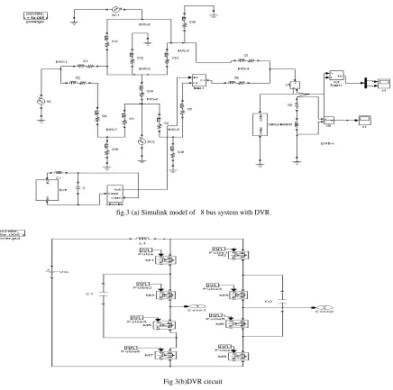
A typical DVR built in MATLAB and installed into a simple power system to protect a sensitive load in a large distribution system is presented. Coupling transformer with either a delta or wye connection on the DVR side is installed on the line in front of the protected load. Filters can be installed at the coupling transformer to block high frequency harmonics caused by DC to-AC conversion to reduce distortion in the output [5]. The DC voltage source is an external source supplying DC voltage to the inverter. The optimization of the DC source can be determined during simulation with various scenarios of control schemes, DVR configurations, performance requirements, and voltage sags experienced at the point DVR is installed.
fig.3 (a) Simulink model of 8 bus system with DVR
4. Simulation Results
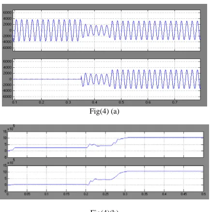
In order to understand the performance of the DVR along with control, 8 bus system as shown in Figure(4) is implemented. Voltage sags are simulated by temporary connection of different impedances at the load side bus. A DVR is connected to the system through a series transformer with a capability to insert a maximum voltage of 50% of the phase to-ground system voltage.. The results are shown in Figure [5]. A 30% voltage sag is initiated at 200 ms and it is kept until 400 ms, with total voltage sag duration of 200ms.. Observe that during normal operation, the DVR is doing nothing. It quickly injects necessary voltage components to smooth the load voltage upon detecting a voltage sag. It is noted that voltage harmonics in voltage source inverter are0.10%
Fig(4) (a)
Fig(4)(b)
Simulation result of DVR response to an balanced voltage sag using V-source inverter (a)Voltage across load-1and load2 (b) Real & reactive power in load-1
Fig(5) Fast fourier Transformation Analysis(FFT) of output voltage
Table [1] Voltage harmonics for different values of phase shift (
)
Voltage harmonics Harmonic eliminated
order Without
filter
With filter
Degree (%) (%) n 25.5 24.0 0.13 7th
5.Experimental Results
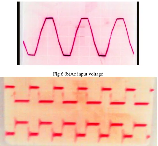
A prototype of the proposed DVR was built and tested to confirm the feasibility of the hardware implementation, based on the simulation results. The prototype is composed of two full-bridge inverters to control each phase voltage, a gate drive circuit, a super-capacitor bank, a power transformer, an anti-parallel thyristor switches, a display circuit, and a microcontroller as shown in Fig.6(a). The proposed DVR sets the operation frequency automatically by checking the source voltage when the system starts up. All operations are carried out automatically when the main switch is turned on. The load voltage maintains a constant value as confirmed by the simulation results. Fig 4(a). shows an expanded waveform focusing on the sag beginning point. The load voltage is restored within 2.0ms as confirmed by the simulation results. This delay is due to the sag detection time and the turn-off time of the MOSFET switches. Also, it can be seen that the output voltage contains much less harmonics. Hardware layout is shown in Fig 6a and AC input voltage is shown in Fig 6b.
Fig 6 (a)Three level based DVR
Fig 6 (b)Ac input voltage
Fig 6(d) Three level output
Fig 6(e) output of DVR after LC filter
6. CONCLUSION
This paper has presented a DVR system based on the V-source inverter. The operating principle, analysis and the harmonic contents are presented. In summary, the V-source inverter DVR system has several unique advantages that are very desirable for many DVR applications,
* it can produce any desired output ac voltage, even greater than the line voltage
* Provides ride through during voltage sags without any additional circuits and energy storage; * reduces in-rush and harmonic current.
*unique features include improved reliability, strong EMI immunity, and low EMI *The voltage source technology is applied to the entire spectrum of power conversion.
*Experimental results coincide with the simulation results.
References
[1] A. Ghosh and G. Ledwich, Power Quality enhancement Using Custom Power Devices, Kluwer Academic Publishers, 2002.
[2] S. Santoso, Electrical Power System Quality, Mcgraw-Hill, 2002.
[3] N.G. Hingorani, Introducing Custom Power, in IEEE Spectrum,32, pp. 4l-48, 1995.
[4] P. T. Nguyen and T. K. Saha (2004), “DVR against balanced and unbalanced Voltage sags: Modeling and simulation,” IEEE-School of
Information Technology and Electrical Engineering, University of Queesland, Australia, 2004.
[5] Yop Chung, Dong-Jun Won, Sang-Young Park, Seung-Il Moon andJong-Keun Park; ”The DC link energy control method in dynamic
voltage restorer system”, International journal on Electric power and energy system, Volume 25, Issue 7, september 2003, Pages 525-531
[6] Paisan Boonchiam and Nadarajah Mithulananthan, “Understanding of Dynamic voltage Restorers Through MATLAB Simulation”
Thammasat Int. J. Sc. Tech., vol.11, No. 3, July-September 2006.
[7] B. Justus Rabi and R. Arumugam,” Harmonics Study and Comparison of Z- Source Inverter with Traditional Inverters”, American Journal
of Applied Sciences 2 (10): 1418-1426, 2005.
[8] Miaosen Shen, Alan Joseph, Jin Wang, Fang Z. Peng1, and Donald J. Adams2, ” “comparison of Traditional Inverters and Z- Source
Inverter for Fuel Cell Vehicles”.
[9] F. Z. Peng, “ Z-Source Inverter,” in Proc. IEEE IAS’02,2002. pp.775 – 781.
About Authors
S.DEEPA has obtained her B.E degree from Periyar University in 2003. She has obtained her PG degree from Annamalai University in 2005. Presently she is doing her research at Sathyabama University. Her research interest is in the area of Power quality.
![Fig. [2] Equivalent circuit of DVR](https://thumb-us.123doks.com/thumbv2/123dok_us/9618353.1490033/2.612.207.405.192.326/fig-equivalent-circuit-of-dvr.webp)