Italian Journal of Science & Engineering
Vol. 1, No. 3, October, 2017
An Offset-free High linear Low Power High Speed
Four-Quadrant MTL Multiplier
HoseinAli Jafari
a, Zahra Abbasi
b, Seyed Javad Azhari
a*a Department of Electrical and Electronic engineering, Iran University of Science and Technology, Tehran, Iran b Department of Electrical and Electronic engineering, University of Alberta, Edmonton, Canada
Abstract
In this paper a new CMOS current-mode four-quadrant analog multiplier circuit is proposed. The major advantages of this design are high linearity, high speed and low power consumption. Removing dc offset is the most important improvement in this topology. The circuit is designed with 1.8V supply voltage and is simulated using HSPICE simulator by level 49 parameters in 0.18µm standard CMOS TSMC technology. The aspect ratios of the MOSFETs are optimized using Evolutionary algorithm by MATLAB. The simulation results of this analog multiplier demonstrate a maximum linearity error of 2.6%, a THD of 1.77%, maximum power consumption of 157 µW, -3dB bandwidth of 241MHz and almost free from dc offset.
Keywords:
Current-Mode; Translinear;
CMOS Analog Multiplier; Offset Free.
Article History:
Received: 10 September 2017
Accepted: 30 October 2017
1-
Introduction
Todays, multiplier circuits, especially the four-quadrant ones, are frequently used in such wide range of applications as automatic gain control, phase locked loop, modulation, detection, adaptive filters, square rooting of signals, FPAAs, and neural networks [1, 2]. In all these mentioned application, power consumption plays a major role while, using current-mode technique has proved to highly reduce this major parameter [3, 4].
High speed, low-power, low voltage and well linear multipliers have to be designed by specific structures and technologies. CMOS analog technology is widely recognized as the most desirable technology and method to design this very important block. Several multiplier circuits have been designed using different techniques to reduce power consumption and nonlinearity as the two most important parameters of this circuit. However, they suffer from such problems as low speed and large DC offset. In the multiplier circuits of [2-4] power consumption is very high and the bandwidth is not enough for high speed applications. In [1, 3] the offset error is such considerable that the output is not suitable for high accuracy applications.
2-
Structure and Theoretical Analysis of the Proposed Multiplier
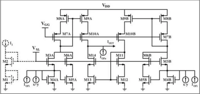
The proposed multiplier circuit is shown in Figure1. This circuit is driven by a bias part consisting M1 and M2 diode
connected MOSFETs that secures VSL as the bias voltage of main part of the circuit. Alternatively, VSL (also VGG) can
be provided by VDD through a suitable divided resistor network. Current sources of (x-y) and (x+y) are the input signals
of this circuit and IOfo and IOfi are the current sources to cancel the offset errors as will be further discussed later. One of
the most important nonidealities of the Mos transistors that mainly causes current errors and nonlinearity in current mirror blocks is channel modulation problem. It is regularly produced by either unequal VDS of basic pair transistors of
the current mirror (i.e. M4A-M5A, M4B-M5B and the like here) or/and low output impedance of the current mirror. To
guarantee both above-mentioned privileges to sustain, transistors M3A, M6A, M14, M6B ,M3B in bottom half and the likes
in top half of the multiplier are inserted. In addition, high swing low voltage cascode current mirrors are used to further
* CONTACT: [email protected]
increase the dynamic range and reduce the distortion of the proposed circuit. Thus elaborately realizing all above explained plans has greatly secured the less current error and nonlinearity of the proposed multiplier.
Now assuming all transistors of this structure are well matched, working in saturation region and have the same trasconductance parameters, then applying MTL translinear principle to both traslinear loops of M1, M2, M3A, M4Aand
M1, M2, M3B, M4B in saturation region [5] gives:
Figure 1. Proposed current-mode analog multiplier circuit
1 3 4
2
I
I
A
I
A (1-A)1 3 4
2
I
I
B
I
B (1-B)By applying KCL at the input and output nodes :
4A 3A
I
I
x
y
(2-A)4B 3B
I
I
x
y
(2-B)10 14
OUT A
I
I
I
(3)On the other hand:
6A 5A 4A 3A
I
I
I
I
x
y
(4-A)6B 5B 4B 3B
I
I
I
I
x
y
(4-B)Then to relate output current to input ones and bias current of I1, Equation 3. is expanded as:
14 12 10 7 6 3 3
10 7 6 3 3
2
2
M B M B B B B
A M A A A A
I
I
I
I
I
I
I
x
y
I
I
I
I
I
x
y
(3-A)3 6 3 6 3 3
(
) (
)
2
2
2
OUT A A B B A B
I
I
I
I
I
I
I
y
(3-B)Substituting (2-A) in (1-A) and squaring both sides gives:
1 3 3 3
4
I
2
I
A
(
x
y
)
2
I
A(
I
A
x
y
)
(5)Then Squaring (5) and simplify the result yields: 2
1 3
1
(4
(
))
16
AI
x
y
I
I
(6-A)2 1
3
1
(4
(
))
16
BI
x
y
I
I
(6-B)Substituting (6-A) , (6-B) in (3-B) produces:
2 2
1 1
1 1
(4
(
))
(4
(
))
(
(
)) (
8
8
(
))
OUT
I
x
y
I
x
y
I
x
y
I
I
x
y
(7) 12
OUTxy
I
I
(8)Equation 8. illustrates that the proposed circuit can either be used as a divider by changing (I1) to a variable parameter
or as a multiplier otherwise. In Some applications where there is no need for division, the bias circuit can be replaced by dc voltage source VSL . Equation 9. illustrates that changing the voltage of VSL affects the output current slope; so,
the slope of the output current would be voltage controlled. However, current controling of the output current can either be achieved by variation of I1 current source.
2
(
)
2
OUT SL OX thxy
I
V
W
C
V
L
(9)The mismatch between NMOS and PMOS transistors and even between the same type of transistors effect of VDS on
drain current plus imbalance between pathes fom input to output cause unexpected phenomena such as offset. Offset can change the circuit’s output response and is one of the significant source of error in the circuit. As it is shown in Figure.2, the crossing point is not exactly on zero and the more is the deviation of this crossing point from zero the larger would be the offset value. This offset consists of two components. To cancel this unwanted phenomena, two offset currents of IOfi and IOFo are applied to the proposed circuit as is shown Figure 1. These offset currents affect the
offset of the circuit by changing the current coming to the input and output nodes. Changing the input node’s current by IOfi reduces horizontal offset and change the current in the output by IOFo decreases vertical offset.In practice, these
compensating offset values should be applied off chip to the same shown points by proper tunable intermediate current sources. The simpelest tuneable current source which can generate offset currents is shown in Figure 3. in which, by changing POTref as a tunable resistance,the output current can be changed.
3-
Simulation Results
To verify the performance of the proposed circuit of Figure1. HSPICE is used to simulate the proposed circuit using level 49 parameters in 0.18 𝑢𝑚 standard CMOS TSMC technology and 1.8V supply voltage.the aspect ratios of MOS transistors are listed in table.1 the values of which are optimized by such evelotionary algorithm as is described in [6]. The bias values of the circuit are also given in Table 2.
Table 1. Aspect Ratio of Figure 1. MOSFETs in micrometer
M3A, M4A, M5A, M3B, M4B, M5B 5.4/0.54
M9A, M10A, M9B, M10B, M13, M14 18/0.18
M11, M12 10/0.54
M6A, M6B 26/0.18
M7A, M7B 10/0.54
M8A, M8B 12.85/0.54
Table 2. Bias Values
VSL 1V
I1 10 µA
VGG 1V
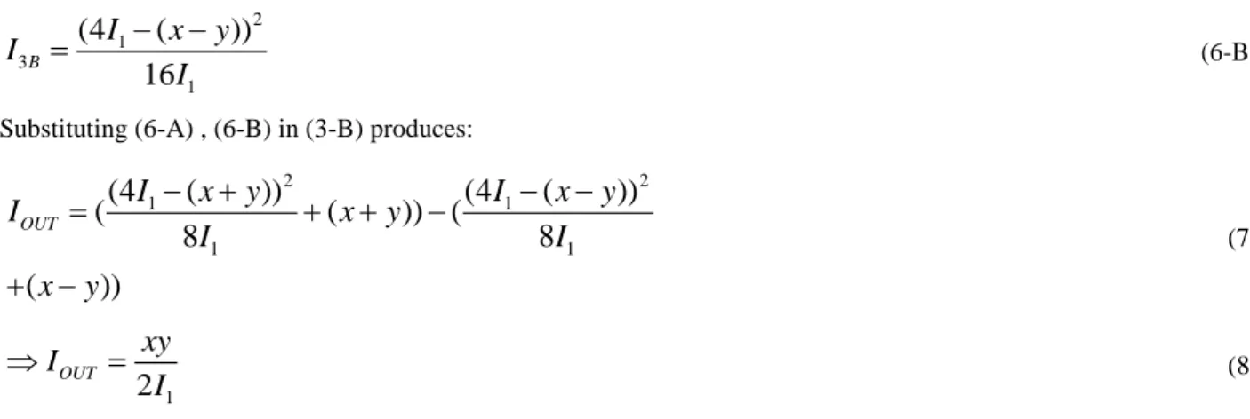
Figure 4. Simulation result of proposed current multiplier circuit and error measurement
The input signals are the sine function with different frequencies of 1 and 10 𝐾𝐻𝑧. As can be seen in Figure 4, the maximum error is less than 2.5%.
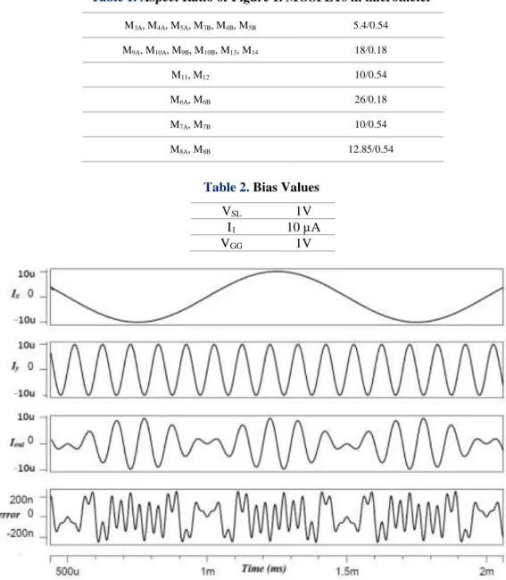
Figure 5. VSL effect on the output current slope
The offset canceled DC transfer function which has the most linear response is shown in Figure 6.
Figure 6.Offset canceled DC transfer characteristics
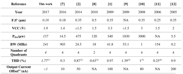
Table 3. Comparison between this work and other reported papers
Reference This work [7] [2] [8] [1] [9] [10] [11] [12]
Year 2017 2016 2014 2010 2009 2009 2008 2006 2005
F.S (µm) 0.18 0.18 0.35 0.5 0.35 NA 0.35 0.25 0.35
VCC (V) 1.8 1.4 ±1.5 1.5 3.3 ±1.5 3 1.5 2
Pdiss(µw) 157 14.5 475 120 340 1830 3000 NA 5.5
BW (MHz) 241 903 24.5 18 41.8 53.1 1 154 0.2
Number of
Quadrants 4 4 4 2 4 4 4 4 4
THD (%) 1.77(1) 0.3 0.87(2) 0.63(3) 0.97 1.39(4) 1(5) 0.25(6) 0.9
Output Current
Offset(nA) <1 10 50 NA 100 NA 80 NA 200
(1) f=1 MHz at 100% bias, 10 µA (2) I
x=20 µA (3) Ix=50 µA (4) f=100 KHz (5) f=1 KHz (6) f=1 MHz
* Feature Size
**The mentioned refrences do not report the exact quantity of this offset; however, this offset can be underestood approximately from DC transfer characteristics figure
4-
Conclusion
In this brief, a four quadrant CMOS current-mode multiplier circuit was proposed. The performance of the multiplier has been simulated using HSPICE software. The advantages of the proposed analog multiplier circuit are high speed, low power consumption and removed dc offset. These distinct achievements and improvements makes the proposed schematic appropriate for very precise and high bandwidth applications.
5-
References
[1] A. Naderi, A. Khoei, K. Hadidi, and H. Ghasemzadeh, “A new high speed and low power four-quadrant CMOS analog multiplier in current mode,” AEU - Int. J. Electron. Commun, vol. 63, no. 9, pp. 769–775, Sep. 2009.
[2] N. Beyraghi, A. Khoei, and K. Hadidi, “CMOS design of a four-quadrant multiplier based on a novel squarer circuit,” Analog Integr. Circuits Signal Process, vol. 80, no. 3, pp. 473–481, Sep. 2014.
[3] C. Popa, “Improved Accuracy Current-Mode Multiplier Circuits with Applications in Analog Signal Processing,” IEEE Trans. Very Large Scale Integr. VLSI Syst., vol. 22, no. 2, pp. 443–447, Feb. 2014.
[4] C. Sawigun and W. A. Serdijn, “Ultra-low-power, class-AB, CMOS four-quadrant current multiplier,” Electron. Let, vol. 45, no. 10, pp. 483–484, May 2009.
[5] C. Toumazou, F. J. Lidgey, and D. Haigh, Analogue IC design: the current-mode approach, vol. 2. Presbyterian Publishing Corp, 1990.
[6] B. Liu et al., “Analog circuit optimization system based on hybrid evolutionary algorithms,” Integr. VLSI J., vol. 42, no. 2, pp. 137–148, Feb. 2009.
[7] M. M. Maryan, S. J. Azhari, and M. R. Hajipour, “A simple low-power high-speed CMOS four-quadrant current multiplier,” in 2016 24th Iranian Conference on Electrical Engineering (ICEE), 2016, pp. 1471–1474.
[8] A. J. Lopez-Martin, C. A. D. L. C. Bias, J. Ramirez-Angulo, and R. G. Carvajal, “Compact low-voltage CMOS current-mode multiplier/divider,” in Proceedings of 2010 IEEE International Symposium on Circuits and Systems, 2010, pp. 1583–1586. [9] N. Pisutthipong and M. Siripruchyanun, “A novel simple current-mode multiplier/divider employing only single multiple-output current controlled CTTA,” in TENCON 2009 - 2009 IEEE Region 10 Conference, 2009, pp. 1–4.
[10] M. B. Machado, A. I. A. Cunha, C. G. Montoro, and M. C. Schneider, “Trans conductance-based CMOS analog multiplier,” in 2008 Joint 6th International IEEE Northeast Workshop on Circuits and Systems and TAISA Conference, 2008, pp. 367–370. [11] P. Prommee, M. Somdunyakanok, M. Kumngern, and K. Dejhan, “Single Low-Supply Current-mode CMOS Analog Multiplier Circuit,” in 2006 International Symposium on Communications and Information Technologies, 2006, pp. 1101–1104.