New Considerations for MOSFET Power Clamps
Steven S. Poon and Timothy J. Maloney
Intel Corporation, SC12-607, 2200 Mission College Blvd., Santa Clara, CA 95052, USA
tel.: (408)765-5574, fax: (408)765-4716, e-mail: [email protected]
This paper is co-copyrighted by Intel Corporation and the ESD Association
Abstract - Two ESD clamp circuit design techniques have been developed to reduce cell size and to combat the
effects of gate leakage that have become significant in recent generations of digital CMOS process technology. Such clamps have proven to be able to withstand HBM stresses of 6kV and CDM pulses of 1.2kV.
I. Anti-Gate Leakage PMOS
Power Clamps
I.a. Introduction
Having been used widely and successfully on a large number of high-volume silicon integrated circuit products for many process generations, PMOS power clamps are known to be successful in protecting power and input/output pins from electrostatic discharge (ESD) excursions, even when designed with minimum effort. Recent generations of device fabrication technology, however, have accentuated device properties that were considered negligible and irrelevant for the design of ESD clamp circuits. In
SDUWLFXODU DW WKH P DQG P WHFKQRORJ\
nodes, many reported processes [1-2] have scaled the thickness of the gate dielectric to such an extent that gate tunneling current increases by orders of magnitude, which further varies significantly at different process corners. The high gate current can render standard ESD power supply clamps [3] non-functional, necessitating modifications to existing circuits to minimize sensitivity to the leakage. This first part of the paper will show the circuit changes needed to combat the gate leakage, as well as the silicon test results confirming the success of the new designs.
I.b. Discussion
The debilitating effects of excessive gate current on ESD power supply clamps can be explained with the help of Fig. 1. An RC timer is typically used to enable the clamp during fast-edge ESD events and to isolate it from the power supply during power-up and
normal operation. The time constant of the timer is typically set to at least 1-2 VHF WR DOORZ VXIILFLHQW time for ESD events to settle. Such a time constant requires fairly large resistance and large capacitance. Consequently, MOS capacitors with leaky gate dielectric are often more area-efficient than metal or metal-poly capacitors. As shown in Fig. 2, the weak drive and the large leakage can prevent the RC timer from reaching a high enough voltage needed to turn off the clamp for normal operation. The immediate solutions to the problem are to reduce the size of the capacitor, to decrease the resistance of the timer, and to lower the switching threshold of the inverter. All three approaches can restore functionality at the expense of the time constant of the RC timer. It also becomes imperative that one examines the dependence of gate tunneling current on temperature, voltage, and device geometry variations, as there could be a malfunction at a process corner. But even if the clamp were able to turn off, the relatively low timer voltage will keep both the n- and p-channel devices of the timer inverter partially on, resulting in significant standby current - an unproductive use of power. With the increased popularity of low-power products such as mobile devices, the extra leakage alone is enough incentive to search for a solution to the problem.
drive of the RC timer and prevents the circuit from converging to an undesirable voltage. The level restorer device turns on completely when the timer voltage reaches the switching threshold of the inverter, and drives the timer node to a high enough voltage such that standby current is significantly reduced. This approach to the gate-leakage problem has the advantage of simplicity and has proven effective in a mass production environment.
Figure 1: Typical PMOS Power Clamp
0 0.2 0.4 0.6 0.8 1 1.2 1.4 1.6 1.8 2
0.0E+00 5.0E-07 1.0E-06 1.5E-06 2.0E-06
Time [Sec]
Ti
mer V
o
lt
age [V
]
Figure 2: Simulated Timer Output Voltage (2V Power Supply Voltage Step)
Figure 3: Anti-Gate Leakage PMOS Clamp
One potential drawback of the anti-gate leakage clamp is that the strong feedback device decreases the time constant of the RC timer after the power supply has been fully ramped-up. Consequently, the clamp will most likely not respond if an ESD event were to occur after the chip is powered-up and operating. This change in behavior is acceptable, as the PMOS clamp is not a surge protector; its role is predominately to prevent yield loss due to ESD during the manufacturing process.
Another potential problem is that the timer voltage might not be able to reach even close to the inverter switching threshold if the gate leakage of future process technologies becomes truly excessive. In that case, the level restorer will not be able to ensure functionality, as it is able to provide voltage-dependent current only if the timer voltage is near the inverter switching threshold. Additional circuit innovation will become necessary in such an extreme case, though the level restorer will still be useful in decreasing leakage current in the same manner as discussed above.
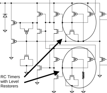
Figure 4: High Voltage-Tolerant Clamps with Level Restorers
The same circuit technical used in Fig. 3 can be applied to high voltage-tolerant MOS power supply clamps [5], which are essentially cascode-connected current drivers with self-generated bias voltages. When not driving ESD current, the circuit provides bias voltages that reduce the voltage stress across each oxide to merely a fraction of the power supply voltage. As shown in Fig. 4, the level restorers can again be used to supply current to the RC timers of the high voltage clamp. One can easily generalize such a scheme to clamps with more cascode stages, which
RC Timer
Steady-state timer output voltage below inverter switching threshold
Timer Level Restorer
involves nothing but applying a level restorer to the RC timer of each stage.
I.c. ESD Testing Results
0 1 2 3 4 5
0 2 4 6 8 10
Sustained Voltage [V]
TLP
Curre
nt
[
A
]
Modified Clamp - 130 nm technology
Unmodified Clamp - 180 nm technology
Figure 5: Measured TLP I-V Characteristics of PMOS Clamps
Temperature Current [ A]
[C] Old Clamp @1.3V New Clamp @ 1.3V
25 366 25.2
125 644 32.0
Table 1: Measured Leakage of PMOS Clamps
The ESD power clamp shown in Fig. 3 has been fabricated using a 130 nm-generation process with dual damascene copper interconnects. Human Body Model (HBM) and Charged-Device Model (CDM) tests have been carried out using the Keytek Zapmaster tester. The anti-gate leakage clamp is able to withstand HBM pulses of above 6 kV and CDM stresses of at least 1.2 kV in both polarities. Both numbers are comfortably above most manufacturing requirements observed by the industry. Fig. 5 shows the current-voltage characteristics of the clamp measured through transmission line pulsing (TLP) [6]. Compared to an unmodified clamp used in a 180 nm-generation process (with larger area), the new clamp with anti-gate leakage provisions clearly has not sacrificed any performance at ESD conditions for functionality at steady state, and is actually smaller due to the process shrink.
Leakage measurements have also been carried out on both the original PMOS clamp circuit (Fig. 1) and the modified anti-gate leakage clamp (Fig. 3), both made with the 130 nm-generation process. Because the two clamps have similar device sizes, any differences in leakage can be attributed to anti-gate leakage modifications. The data shown in Table 1 confirms
that the level-restorer is able to reduce overall clamp leakage by a significant amount, as intended. At higher temperatures and voltages, the original clamp becomes non-functional.
In addition to ESD, power-up, and leakage tests, high volume manufacturing (HVM) products also have to go through an exhausive series of latch-up, burn-in, and other reliability tests. The anti-gate leakage PMOS clamp has been proven to be reliable under harsh testing conditions.
II. High Voltage-Tolerant Clamps
with Single RC Timer
II.a. Introduction
Although the high voltage-tolerant clamp in Fig. 4 is known to be fully functional as an ESD-protection circuit, the use of two RC timers that time out simultaneously is not a good use of silicon space. Conceptually, a single RC timer ought to suffice. Also, the dramatic increase in gate tunneling current might, in the future, leave the designer with no choice but to use area-intensive capacitors such as metal or series-connected MOS capacitors. The use of multiple RC timers can therefore result in too large a cell size. We would like to reduce the number of RC timers to the theoretical limit. Techniques to achieve such a goal will be presented below, and silicon data that proves functionality will be disclosed.
II.b. Discussion
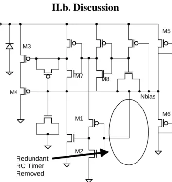
Figure 6: High Voltage-Tolerant PMOS Power with Single RC Timer
Redundant RC Timer Removed
M1
M2
Nbias M3
M4
M5
M6 M7
Shown in Fig. 6 is a high voltage-tolerant MOS clamps design with a single RC timer [7]. The modified circuit retains only the one RC timer closest to the positive power supply, while the rest are removed. The input of the inverter formed by devices M1 and M2, now no longer driven by RC timers, is tied to the node Nbias. If the voltage at Nbias starts at a low enough level at the onset of an ESD event, which can be ensured with a measured amount of capacitance between Nbias and ground, the ESD current-handling devices M3 and M4 will be driven low by the predriver. ESD current flows through the clamp until the single RC timer times out, causing inverters to flip and the large current handling devices to turn off. At this point, little current flows through the predriver and the bias network formed by the weak devices M5 and M6 are able to keep Nbias at half of the power supply voltage, such that all gate-to-source and gate-to-drain voltages stay below technology-defined limits in the long term. As long as the time constant of each RC timer is the same, the events described above will happen within the same amount of time as the turn off time of a PMOS clamp with a multiple-RC timer.
Although the circuit in Fig. 6 is only a two-stack cascode, one can, through applying the same principles described above, remove redundant RC timers from clamps with multiple-cascode stages, much as described in Ref. [5]. This technique may also combine with the anti-gate leakage circuits presented above to provide robust ESD solutions for processes with leaky oxides.
It is interesting to note that the gate-bulk voltage across M8 is still as high as the power supply voltage at steady-state, and at first glance might be considered worrisome. However, since a conductive channel is induced under the gate of each device operating in the “on” state, the voltage across the oxide of such a device will be at most half of the power supply voltage along the whole length of the channel. The depletion region between the inverted channel and the bulk will then sustain the rest of the gate-bulk voltage, which is usually not a reliability concern.
Although high body bias does not defeat the purpose of the voltage-tolerant clamps, it can still produce secondary effects that are of interest to the design of the circuit. As process technologies move towards more aggressive implant strategies in order to combat short channel effects, p-n junction leakage can become significantly higher than before. Such an increase has implications for high voltage-tolerant clamps, as several devices in the clamps may have
high bulk voltages with respect to other device terminals, which can potentially trigger band-to-band tunneling mechanisms such as gate-induced drain leakage (GIDL) and source/drain-to-halo implant zener breakdown. Some junction leakage paths in Fig. 6 include the n-well/drain junction of M4 and the drain/substrate junction of M7. Because of its sheer size, the junction leakage through the drain of M4 is likely to be the most important to address. One way to reduce such unwanted leakage is to separate the well that houses M3 and M4 such that each device has its own well that is connected to its individual source. This configuration reduces the reverse-bias voltage between the well and the drain at the cost of some area. It also now frees us to choose M3 and M4 of arbitrary size, as the devices are now separated from a layout point of view. To find the optimal sizes, we present a simple analysis. From Kirchoff’s current law and the classic textbook equations:
ds ds t gs d V V V V z I ) 2 ( − −
= if Vds >Vgs −Vt
2 ) (
2 gs t
d V V
z
I = − if Vds <Vgs −Vt
where Id is the drain current, Vgs is the gate voltage,
ds
V
is the drain voltage,V
t is the threshold voltage,and
z
i is directly proportional to the width of the ith
transistor. Then one can show that
∑
= − = n i i t n d z V V I 1 2 1 2 ) (where n is the number of devices in the stack, or 2 in this case. Thus the ESD pulse current can be
maximized if the sum
∑
i zi
1
is minimized. This
happens when the widths of all devices in the stack are equal, as can be shown with the Method of Lagrange Multipliers.
II.c. ESD Testing Results
in Fig. 7, it is clear that both clamps function properly when excited by sudden current pulses.
0 1 2 3 4 5
0 2 4 6 8 10
Sustained Voltage [V]
TLP
Cur
re
nt [A]
2-Stack Single RC Clamp 3-Stack Single RC Clamp
Figure 7: TLP I-V Characteristics of Single RC Power Clamps
III. Conclusion
Because of increased gate tunneling current intrinsic to deep sub-micron CMOS technologies with ultra-thin oxides, standard power supply ESD-protection clamp circuits can malfunction and need adjustment. The clamp circuit can be modified so that more current is provided to the leaky oxides when needed. In addition, a new method to reduce the size of voltage-tolerant power supply clamps for ESD protection is presented. The reduction is done by reformulating the circuit and by removing certain redundant circuit elements with significant size. Both circuit techniques have enabled the fabrication of robust ESD clamps that are proven to give good ESD performance.
Acknowledgements
The authors would like to thank Tina Cantarero for the ESD testing data. They also thank Andrew Volk and Marty Agostinelli for their valuable inputs.
References
[1] S. Tyagi et al., “A 130 nm Generation Logic Technology Featuring 70 nm Transistors, Dual Vt Transistors and 6 Layers of Cu Interconnects”, IEDM Tech. Digest, 2000, pp. 567-570.
[2] L. K. Han et al., “A Modular 0.13 µm Bulk CMOS Technology for High Performance and Low Power Applications”, VLSI Tech. Digest, 2000, pp. 12-13. [3] T.J. Maloney, "Designing Power Supply Clamps for Electrostatic Discharge Protection of Integrated Circuits", Microelectronics Reliability 38, No. 11, pp. 1691-1703 (November, 1998).
[4] T.J. Maloney and W. Kan, "RC Timer Scheme", US Patent application, filed by Intel June 30, 2000. [5] T.J. Maloney and W. Kan, "Stacked PMOS Clamps for High Voltage Power Supply Protection", 1999 EOS/ESD Symposium Proceedings, pp. 70-77. Also published in Microelectronics Reliability 41, No. 3, pp. 335-348 (March, 2001).