DESIGN OF A HIGH PERFORMANCE AND LOW POWER EXPLICIT PULSE
TRIGGERED FLIP FLOP
A.PAVAN KUMAR1 M.GOPALA KRISHNA2
1
M.tech Student, DVR & DHS MIC College of Technology, Kanchikacherla, Andhra Pradesh, INDIA.
2
Assistant Professor, Dept. of ECE, DVR & Dr. HS MIC College of Technology, Kanchikacherla, AP, INDIA.
Abstract- A low-power flip-flop (FF) design
featuring an explicit type pulse-triggered structure and a modified true single phase clock structure based on a signal feed-through scheme using transmission gate is presented, where the circuit of the existing method is modified for low power dissipation and to reduce the number of transistor count. The proposed design successfully solves the long discharging path problem in conventional explicit type pulse-triggered flip-flop (ep-FF) designs and achieves better speed and power performance. Based on simulation results using BSIM4 Model CMOS 90-nm technology, the proposed design outperforms the conventional explicit type P-FF design data-close-to-output (ep-DCO). In the mean time, the performance edges on power metrics are improved
Index Terms—Flip-flop (FF), low power,
pulse-triggered, transmission gate. I. INTRODUCTION
Flip-flops (FFs) are the basic storage elements used extensively in all kinds of digital designs. In particular, digital designs nowadays often adopt intensive pipelining techniques and employ many FF-rich modules such as register file, shift register, and first in first out. It is also estimated that the power consumption of the clock system, which consists of clock distribution networks and storage elements, is as high as 50% of the total system power.
FFs thus contribute a significant portion of the chip area and power consumption to the overall system design. Pulse-triggered FF (P-FF), because of its single-latch structure, is more popular than the conventional transmission gate (TG) and master– slave based FFs in high-speed applications. Besides the speed advantage, its circuit simplicity lowers the power consumption of the clock tree system. A P-FF consists of a pulse generator for strobe signals and a latch for data storage. If the triggering pulses are sufficiently narrow, the latch acts like an edge-triggered FF. Since only one latch, as opposed to two
in the conventional master–slave configuration, is needed, a P-FF is simpler in circuit complexity. This leads to a higher toggle rate for high-speed operations. P-FFs also allow time borrowing across clock cycle boundaries and feature a zero or even negative setup time. Despite these advantages, pulse generation circuitry requires delicate pulse width control to cope with possible variations in process technology and signal distribution network.
PF-FFs, in terms of pulse generation, can be classified as an implicit or an explicit type. In an implicit type P-FF, the pulse generator is part of the latch design and no explicit pulse signals are generated. In an explicit type P-FF, the pulse generator and the latch are separated. This concept is illustrated in fig. 1. Without generating pulse signals explicitly, implicit type P-FFs is in general more power-economical. However, they suffer from a longer discharging path, which leads to inferior timing characteristics. Explicit pulse generation, on the contrary, incurs more power consumption but the logic separation from the latch design gives the FF design a unique speed advantage. Its power consumption and the circuit complexity can be effectively reduced if one pulse generator is shares a group of FFs (e.g., an n-bit register).
Fig. 1: Illustration of explicit pulse triggered flip flop
II.CONVEVTIONAL EXPLICIT TYPE PULSE TRGGERED FLIP FLOP (P-FF) DESIGNS
In this brief, we will thus focus on the explicit type P-FF designs only. To provide a comparison, some existing P-FF designs are reviewed first.
A. EP-DCO
Fig. 2 shows a classic explicit P-FF design, named data-close to- output (ep-DCO). It contains a NAND-logic-based pulse generator and a semi dynamic true-single-phase-clock (TSPC) structured
latch design. In this P-FF design, inverters x8 and x9 are used to latch data, and inverters x6 and x7 are used to hold the internal node X.
Fig.2: Explicit type data closed to output pulse triggered flip flop (EP-DCO).
The pulse width is determined by the delay of three inverters. This design suffers from a serious drawback, i.e., the internal node X is discharged on every rising edge of the clock in spite of the presence of a static input “1.” This gives rise to large switching power dissipation. To overcome this problem, many remedial measures such as conditional capture, conditional precharge, conditional discharge, and conditional pulse enhancement scheme have been proposed.
B. CDFF
Fig. 3 shows a conditional discharged (CD) technique. An extra nMOS transistor controlled by the output signal Q_fdbk is employed so that no discharge occurs if the input data remains “1.” Hence switching power is reduced.
Fig. 3: Conditional discharges flip flop (CDFF) In addition, the keeper logic for the internal node X is simplified and consists of an inverter plus a pull-up pMOS transistor only. If the input is changes from “0” to “1” the internal node X is discharged through M12, M14 and M16 as assuming that
(Q,Q_fdbk) were initially (low, high). As internal node X is discharged it pulled M10 is ON and the output will be charged. If the input changes from “1” to “0” then the first stage is disabled and node X retains its precharge state and output Q is discharged. Since node X is not charging and discharging periodically at every cycle at every cycle no gliches will appear at output Q when input data stays high.
C. STATIC-CDFF
Fig. 4 shows a similar P-FF design (SCDFF) using a static conditional discharge technique. It differs from the CDFF design in using a static latch structure. Node X is thus exempted from periodical precharges. It exhibits a longer data-to-Q (D-to-Q) delay than the CDFF design. Both designs face a worst case delay caused by a discharging path consisting of three stacked transistors at first stage of flip flop. To overcome this delay for better speed performance, a powerful pull-down circuitry is needed, which causes extra layout area and power consumption.
Fig. 4: Static Conditional discharges flip flop (STATIC-CDFF)
D. MHLFF
The modified hybrid latch flip flop (MHLFF) shown in Fig. 5 also uses a static latch. The keeper logic at node X is removed. A weak pull-up transistor MP1 controlled by the output signal Q maintains the level of node X when Q equals 0. Despite its circuit simplicity, the MHLFF design encounters two drawbacks. First, since node X is not pre-discharged, a prolonged 0 to 1 delay is expected. The delay deteriorates further, because a level-degraded clock pulse (deviated by one VT) is applied
to the discharging transistor MN3. Second, node X becomes floating in certain cases and its value may drift causing extra dc power. And larger transistor MN1 and MN2 is required to enhance the discharge capability.
E. TSPCFF
The fig. 6, this design adopts a signal feed-through technique to improve the delay. Similar to the SCDFF design, the proposed design also employs a static latch structure and a conditional discharge scheme to avoid superfluous switching at an internal node. However, there are three major differences that lead to a unique TSPC latch structure and make the proposed design distinct from the previous one. First, a weak pull-up pMOS transistor MP1 with gate connected to the ground is used in the first stage of the TSPC latch. This gives rise to a pseudo-nMOS logic style design, and the charge keeper circuit for the internal node X can be saved.
Fig.5: Modified hybrid latch flip flop (MHLFF)
Fig.6: True single phase clock latch flip flop (TSPC) In addition to the circuit simplicity, this approach also reduces the load capacitance of node X. Second, a pass transistor MNx controlled by the pulse clock is included so that input data can drive node Q of the latch directly (the signal feed-through scheme). Along with the pull-up transistor MP2 at the second stage inverter of the TSPC latch, this extra passage facilitates auxiliary signal driving from the input source to node Q. The node level can thus be quickly pulled up to shorten the data transition delay. Third, the pull-down network of the second stage inverter is completely removed. Instead the newly employed pass transistor MNx provides a discharging path. The role played by MNx is thus twofold, i.e.,
providing extra driving to node Q during 0 to 1 data transitions, and discharging node Q during “1” to “0” data transitions. Compared with the latch structure used in SCDFF design, the circuit savings of the proposed design include a charge keeper (two inverters), a pull-down network (two nMOS transistors), and a control inverter. The only extra component introduced is an nMOS pass transistor to support signal feedthrough. This scheme actually improves the “0” to “1” delay and thus reduces the disparity between the rise time and the fall time delays. In comparison with other P-FF designs such as ep-DCO, CDFF, and SCDFF, this design shows the most balanced delay behaviors.
III TRANSMISSION GATE TECHNOLOGY
In principle, a transmission gate made up of two field effect transistors, in which in contrast to traditional discrete field effect transistors - the substrate terminal (Bulk) is not connected internally to the source terminal. The two transistors, an n-channel MOSFET and a p-channel MOSFET are connected in parallel with this, however, only the drain and source terminals of the two transistors are connected together. Their gate terminals are connected to each other via a NOT gate (inverter), to form the control terminal. The fig. 7 shows CMOS transmission gate.
As with discrete transistors, the substrate terminal is connected to the source connection, so there is a transistor to the parallel diode (body diode), whereby the transistor passes backwards. However, since a transmission gate must block flow in either direction, the substrate terminals are connected to the respective supply voltage potential in order to ensure that the substrate diode is always operated in the reverse direction. The substrate terminal of the p-channel MOSFET is thus connected to the positive supply voltage potential and the substrate terminal of the n-channel MOSFET connected to the negative supply voltage potential. So it conducts strong logic “1” as well a strong logic “0”
When the control input is a logic zero (negative power supply potential), the gate of the n-channel MOSFET is also at a negative supply voltage potential. The gate terminal of the p-channel MOSFET is caused by the inverter, to the positive supply voltage potential. Regardless of on which switching terminal of the transmission gate (A or B) a voltage is applied (within the permissible range), the gate-source voltage of the n-channel MOSFETs is always negative, and the p-channel MOSFETs is always positive. Accordingly, neither of the two transistors will conduct and the transmission gate turns off.
Fig.7 CMOS Transmission Gate
When the control input is a logic one, so the gate terminal of the n-channel MOSFETs is located at a positive supply voltage potential. By the inverter, the gate terminal of the p-channel MOSFETs is now at a negative supply voltage potential. As the substrate terminal of the transistors is not connected to the source terminal, the drain and source terminals are almost equal and the transistors start at a voltage difference between the gate terminal and one of these conducts.
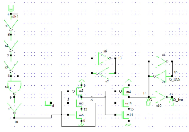
IV PROPOSED EXPLICIT PULSE TRIGGERED FLIP FLOP
The Proposed explicit pulse triggered flip flop is shown in figure 8. It adopts a signal feed-through using transmission gate technique to improve power performances of the TSPC latch structured flip flop based on clock feed through scheme using pass transistor. The proposed design also employs a static latch structure and a conditional discharge scheme to avoid unnecessary switching at an internal node. The only modification done here was instead of pass transistor this design adopts signal feed through using transmission gate.
A transmission gate (combination of MN4 and MP3) controlled by the pulse clock is included so that input data can drive node Q of the latch directly (the signal feed-through scheme). The advantage of transmission gate (TG) over pass transistor is it directly establishes the strong logic 1 and strong logic 0 i.e. full swing at Q, this extra passage facilitates auxiliary signal driving from the input source to node Q by TG is reduces the input to output delay. And transmission gate provides very good isolation between input and output than pass transistor. SO, reverse flows of currents will be eliminated, obviously power dispassion due to those currents will be reduced. The TG will provide both strong „0‟ as well as strong „1‟. In order to provide delay, an inverter is placed at the output to provide feedback to the circuit. No need of charge keeper to preserve the data; so inverter based charge keeper in the existing TSPCL structure flip flop is removed. So, the power consumed by this charge keeper is
saved. In this manner TG reduces the power consumption of the design.
Fig.8 Proposed pulse triggered flip flop The principle of the proposed design is expressed as follows. When a clock pulse arrived is low i.e., logic „0‟, the TG doesn‟t transfer the input data to the output, the output will be the previous data. The principles of FF is when a clock pulse arrives, if no data transition occurs, i.e., the input data and node Q are at the same level, on current passes through the pass TG, which keeps the input stage of the FF from any driving effort. At the same time, the input data and the output feedback Q_fdbk assume complementary signal levels and the pull-down path of node X is off. Therefore, no signal switching occurs in any internal nodes.
When the clock pulse arrived is high i.e., logic „1‟, and the input data D is logic „0‟, the TG will delivers the input data to the output, since TG composed of both NMOS and PMOS, the NMOS will take care of delivering the strong logic „0‟ to the output, the inverted output will given as the feedback to the circuit in order to provide the delay. When the clock pulse arrived is high and the input data D is logic „1‟, the PMOS in TG will take care of delivering the strong logic „1‟ to the output . When the input data, clock and the previous data‟s are high, the data loaded at the FF get discharged through that discharging path.
V SIMULATION RESULTS AND COMPARISON
The simulations of the existing and proposed designs are carried out by using H-SPICE tool using CMOS 90nm technology are shown in below figure 9 to figure 14. By comparing the EP-DCO, CDFF, STATIC-CDFF, MHLFF, TPCFF and Proposed Technique; obtaining the minimized number of transistors and low power consumption; shown in
table 1. And fig. 15 shows the power consumption (in µw) of the existing techniques and proposed technique comparison graph.
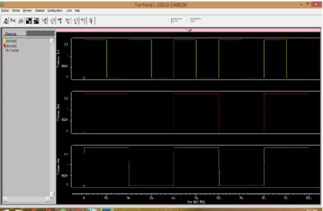
Fig.9: Simulation results of the ep- DCO design
Fig.10: Simulation results of the CDFF design
Fig.11: Simulation results of the Static CDFF design
Fig.12: Simulation results of the MHLFF design
Fig.13: Simulation results of the TSPCL structured design
Fig.14: Simulation results of the proposed design Table I: Comparison of Various P-Ff Designs Flip Flop Design Ep-dco Cdf f Stati c cdff Mh lff Tsp cl Propo sed Number of transistor 28 30 31 19 24 23 Average power (µw) 219 .36 31. 87 28.7 0 11. 26 10. 57 5.65
Fig.15: Comparison graph 0 50 100 150 200 250 power (uw) ep-dco cdff static-cdff mhlff tspclff proposed
VI CONCLUSION
In this paper, presented a novel P-FF design by employing a modeled TSPC latch structure incorporating a mixed design style consisting of transmission gate and pseudo nMOS logic. A new D flip flop is proposed with signal feed through technique using transmission gate, where the circuit of the existing method is modified for low power dissipation and to reduce the number of transistor count. The key idea was to provide a signal feed through from input source to the internal node of the latch, which would facilitate extra driving to enhance both power and speed performance. The design was intelligently achieved by employing a simple transmission gate
VII FUTURE WORK
In future work of the paper, repeat this entire work on the basis of 65nm and 45nm technology nodes or by applying low power techniques like sleepy stack and sleepy keeper techniques we get ultra low power pulse triggered flip flops.
REFERENCES
1. Jin-Fa Lin (2014), “Low-Power PulseTriggered Flip-Flop Design Based on a Signal Feed-Through Scheme,” IEEE Transactions On Very Large Scale Integration (VLSI) Systems, Vol. 22, pp.181185 2. H. Kawaguchi and T. Sakurai, “A reduced clock-swing
flip-flop (RCSFF) for 63% power reduction,” IEEE J. Solid-State Circuits, vol. 33, no. 5, pp. 807–811, May 1998.
3. K. Chen, “A 77% energy saving 22-transistor single phase clocking D-flip-flop with adoptive-coupling configuration in 40 nm CMOS,” in Proc. IEEE Int. Solid-State Circuits Conf., Nov. 2011, pp. 338–339. 4. E. Consoli, M. Alioto, G. Palumbo, and J. Rabaey,
“Conditional pushpull pulsed latch with 726 fJops energy delay product in 65 nm CMOS,” in Proc. IEEE Int. Solid-State Circuits Conf., Feb. 2012, pp. 482–483. 5. H. Partovi, R. Burd, U. Salim, F.Weber, L. DiGregorio,
and D. Draper, “Flow-through latch and edge-triggered flip-flop hybrid elements,” in Proc. IEEE Int. Solid-State Circuits Conf., Feb. 1996, pp. 138–139.
6. F. Klass, C. Amir, A. Das, K. Aingaran, C. Truong, R. Wang, A. Mehta, R. Heald, and G. Yee, “A new family of semi-dynamic and dynamic flip-flops with embedded logic for high-performance processors,” IEEE J. Solid-State Circuits, vol. 34, no. 5, pp. 712–716, May 1999. 7. V. Stojanovic and V. Oklobdzija, “Comparative
analysis of masterslave latches and flip-flops for high-performance and low-power systems,” IEEE J. Solid-State Circuits, vol. 34, no. 4, pp. 536–548, Apr. 1999. 8. J. Tschanz, S. Narendra, Z. Chen, S. Borkar, M.
Sachdev, and V. De, “Comparative delay and energy of single edge-triggered and dual edge triggered pulsed flip-flops for high-performance microprocessors,” in Proc. ISPLED, 2001, pp. 207–212.
9. S. D. Naffziger, G. Colon-Bonet, T. Fischer, R. Riedlinger, T. J. Sullivan, and T. Grutkowski, “The implementation of the Itanium 2 microprocessor,” IEEE J. Solid-State Circuits, vol. 37, no. 11, pp. 1448–1460, Nov. 2002.
10. S. Sadrossadat, H. Mostafa, and M. Anis, “Statistical design framework of sub-micron flip-flop circuits
considering die-to-die and within-die variations,” IEEE Trans. Semicond. Manuf., vol. 24, no. 2, pp. 69–79, Feb. 2011.
11. M. Alioto, E. Consoli, and G. Palumbo, “General strategies to design nanometer flip-flops in the energy-delay space,” IEEE Trans. Circuits Syst., vol. 57, no. 7, pp. 1583–1596, Jul. 2010.
12. M. Alioto, E. Consoli, and G. Palumbo, “Flip-flop energy/performance versus Clock Slope and impact on the clock network design,” IEEE Trans. Circuits Syst., vol. 57, no. 6, pp. 1273–1286, Jun. 2010.
A. Pavan Kumar received Bachelor degree in
Electronics and Communication Engineering from Newtons Institute of engineering in 2013, macherla, Guntur Distirict, AP. He is pursuing the Masters Degree in VLSI & ES from DVR & Dr. HS MIC College of Technology, Kanchikacherla, Krishna District, AP.
M. Gopala Krishna received Bachelor degree in
Electronics and Communication Engineering from Anurag Engineering College in 2009, Kodada, Nalgonda Distirict, Telangana. He also completed his Masters Degree. He is Working as Assistant Professor in DVR & Dr. HS MIC College of Technology, Kanchikacherla, Krishna District, AP.