Dissertations 2017
Application of ASTAR/precession electron
diffraction technique to quantitatively study defects
in nanocrystalline metallic materials
Iman Ghamarian Iowa State University
Follow this and additional works at:https://lib.dr.iastate.edu/etd
Part of theMaterials Science and Engineering Commons, and theMechanics of Materials Commons
This Dissertation is brought to you for free and open access by the Iowa State University Capstones, Theses and Dissertations at Iowa State University Digital Repository. It has been accepted for inclusion in Graduate Theses and Dissertations by an authorized administrator of Iowa State University Digital Repository. For more information, please [email protected].
Recommended Citation
Ghamarian, Iman, "Application of ASTAR/precession electron diffraction technique to quantitatively study defects in nanocrystalline metallic materials" (2017).Graduate Theses and Dissertations. 15522.
Application of ASTAR /precession electron diffraction technique to quantitatively study defects in nanocrystalline metallic materials
by
Iman Ghamarian
A dissertation submitted to the graduate faculty in partial fulfillment of the requirements for the degree of
DOCTOR OF PHILOSOPHY
Major: Materials Science and Engineering Program of Study Committee: Peter C. Collins, Major Professor
Richard A. LeSar Adam J. Schwartz Valery I. Levitas Alexander H. King
Duane D. Johnson
The student author and the program of study committee are solely responsible for the content of this dissertation. The Graduate College will ensure this dissertation is globally
accessible and will not permit alterations after a degree is conferred.
Iowa State University Ames, Iowa
2017
TABLE OF CONTENTS
ACKNOWLEDGEMENTS………..ix
ABSTRACT………...x
CHAPTER 1. INTRODUCTION AND PROBLEM STATEMENT………1
1.1. Motivation……….1
1.2. Contribution of Dissertation……….……….3
1.3. Dissertation Overview……….………..3
CHAPTER 2. BACKGROUND AND LITERATURE REVIEW………5
2.1. Fundamentals of Orientation Descriptors……….……….5
2.1.1. Rotation (orientation) matrix……….……….5
2.1.2. Pole figure and inverse pole figure………9
2.1.3. Euler angles………..…12
2.1.4. Angle/axis of rotation and misorientation…...16
2.1.5. The Rodrigues space………17
2.1.6. Fundamental zone………18
2.2. Orientation Microscopy Techniques……….………...20
2.2.1. Micro-Kossel technique………...20
2.2.2. Kikuchi diffraction pattern………...22
2.2.2.2 Qualitative information extracted from Kikuchi patterns……….26
2.2.2.3 Quantitative information extracted from Kikuchi patterns………...28
2.3. Orientation Microscopy Using ASTAR/Precession Electron Diffraction (ASTAR/PED) Method………...38
2.4. Dislocation Density Distributions for Geometrically Necessary Dislocations………45
2.4.1. Importance of dislocation density determination……….45
2.4.2. Calculations of the dislocation density……….48
2.4.3. Application of the dislocation density calculation method in different materials……….51
2.5. Nanotwins………53
2.5.1. Importance of nanotwin characterization……….53
2.5.2. Characterization of nanotwins………..55
2.6. Grain Boundary Character Distributions……….56
2.6.1. Importance of grain boundary plane studies………56
2.6.2. Analyses of the grain boundary character distributions………...57
2.6.3. Applications of the GBCD method to characterize grain boundaries in different materials….……….61
2.7. Physical Metallurgy……….65
2.7.1. Titanium…….………..65
2.7.1.2 Commercially pure (CP) titanium and alpha titanium alloys………68
2.7.1.3 Alpha/beta titanium alloys……….70
2.7.2. Nickel-based superalloys...74
2.7.3. Zirconium……….76
CHAPTER 3. EXPERIMENTAL AND COMPUTATIONAL METHODS………..78
3.1. Experimental Methods……….78
3.1.1. Sample preparations……….78
3.1.1.1 Ultrafine grained commercially pure titanium alloy……….………78
3.1.1.2 Severely deformed Inconel 617……….80
3.1.1.3 Zirconium thin film………...80
3.1.1.4 Molybdenum trioxide (-MoO3)………...82
3.1.1.5 Surface treated / titanium alloy……….83
3.1.2. ASTAR/precession electron diffraction……….……….…..83
3.1.2.1 Aligning the direct beam…...84
3.1.2.2 Operating the ASTAR/PED system……….…..……….85
3.1.2.3 Indexing the acquired diffraction patterns……….92
3.1.2.4 Determining the absolute orientation of grains………...……102
3.1.3.1 X-ray diffraction………..105
3.1.3.2 Fatigue experiment………...……...105
3.1.3.3 Hardness experiment………...105
3.2. Computational Methods……….106
3.2.1. Dislocation density distributions………106
3.2.2. Grain boundary character distributions………..108
CHAPTER 4. NEW HORIZENS IN CHARACTERIZATIONS BY USING ASTAR/PRECESSION ELECTRON DIFFRACTION AS A STATE-OF-THE-ART ORIENTATION MICROSCOPY TECHNIQUE………..114
4.1. Introduction………....114
4.2. Characterization of the Near-Surface Nanocrystalline Microstructure of UNSM Treated Ti-6Al-4V………....114
4.3. Characterization of Nanotwins in a Severely Deformed Inconel 718 Sample……...133
4.4. Conclusions………....140
CHAPTER 5. DEVELOPMENT AND APPLICATION OF A NOVEL PRECESSION ELECTRON DIFFRACTION TECHNIQUE TO QUANTIFY AND MAP DEFORMATION STRUCTURE IN HIGHLY DEFORMED MATERIALS – AS APPLIED TO ULTRAFINE GRAINED TITANIUM……….………...142
5.1. Introduction………....142
5.2. Raw Data Obtained Using ASTAR/PED Technique………...143
5.3. Dislocation Density Maps and Correlations………..146
5.3.2. Other representation schemes for the processed data……….…150
5.4. Challenges and Limitations………....153
5.4.1. Dislocation density resolution………154
5.4.2. Bend contours……….156
5.5. Conclusions………....160
CHAPTER 6. DETERMINATION OF THE FIVE PARAMETER GRAIN BOUNDARY CHARACTER DISTRIBUTION OF NANOCRYSTALLINE APLHA ZIRCONIUM THIN FILMS………….………..………..162
6.1. Introduction………....162
6.2. Raw Data Acquisition………....162
6.3. Grain Boundary Character Distributions of Alpha Zirconium……….………166
6.3.1. GBCD section about the [0001] axis of misorientation………169
6.3.2. GBCD section about the [2110] axis of misorientation………..172
6.3.3. GBCD section about the [1010] axis of misorientation……….176
6.3.4. 90°/[4131]GBCD section………...182
6.4. Using This Data: Beyond Grain Boundary Engineering………...182
6.5. Conclusions………....183
CHAPTER 7. POSSIBLE FUTURE WORKS………..185
7.2. Poor Angular Resolution……….…………...185
7.3. Dislocation Density Analyses……….…………...186
7.4. Characterization of Grain Boundaries………..………..187
ACKNOWLEDGMENTS
First and foremost, with a deep sense of gratitude, I would like to express my sincere appreciation to my advisor, Dr. Peter Collins, for his endless source of inspiration and encouragement throughout my entire graduate work. He provided me a remarkable freedom to explore novel and exciting research ideas. His far-reaching vision, invaluable support, great guidance and friendship made this dissertation possible.
I would like to thank my committee members Dr. LeSar, Dr. Schwartz, Dr. Levitas, Dr. King and Dr. Johnson for their guidance and support throughout the course of this research. I am also very grateful to Dr. Gregory Rohrer, Dr. Anthony Rollett and Dr. Angus Wilkinson for their invaluable suggestions and comments which have helped me improve the quality of my research.
I would specially thank my everlasting friend, Dr. Peyman Samimi, for his irreplaceable help and support in my research and life while I was a graduate student. I am also thankful to MSE department staff and my fellow graduate and undergraduate students in Dr. Collins group.
Last but certainly not least, I would like to greatly appreciate my parents, Nasir and Fatemeh, for their wonderful support in my entire life.
ABSTRACT
Nanocrystalline metallic materials have the potential to exhibit outstanding performance which leads to their usage in challenging applications such as coatings and biomedical implant devices. To optimize the performance of nanocrystalline metallic materials according to the desired applications, it is important to have a decent understanding of the structure, processing and properties of these materials.
Various efforts have been made to correlate microstructure and properties of nanocrystalline metallic materials. Based on these research activities, it is noticed that microstructure and defects (e.g., dislocations and grain boundaries) play a key role in the behavior of these materials. Therefore, it is of great importance to establish methods to quantitatively study microstructures, defects and their interactions in nanocrystalline metallic materials.
Since the mechanisms controlling the properties of nanocrystalline metallic materials occur at a very small length scale, it is fairly difficult to study them. Unfortunately, most of the characterization techniques used to explore these materials do not have the high enough spatial resolution required for the characterization of these materials. For instance, by applying complex profile-fitting algorithms to X-ray diffraction patterns, it is possible to get an estimation of the average grain size and the average dislocation density within a relatively large area. However, these average values are not enough for developing meticulous phenomenological models which are able to correlate microstructure and properties of nanocrystalline metallic materials. As another example, electron backscatter diffraction technique also cannot be used widely in the characterization of these materials due to
problems such as relative poor spatial resolution (which is ~90 nm) and the degradation of Kikuchi diffraction patterns in severely deformed nano-size grain metallic materials.
In this study, ASTAR/precession electron diffraction is introduced as a relatively new orientation microscopy technique to characterize defects (e.g., geometrically necessary dislocations and grain boundaries) in challenging nanocrystalline metallic materials. The capability of this characterization technique to quantitatively determine the dislocation density distributions of geometrically necessary dislocations in severely deformed metallic materials is assessed. Based on the developed method, it is possible to determine the distributions and accumulations of dislocations with respect to the nearest grain boundaries and triple junctions. Also, the competency of this technique to study the grain boundary character distributions of nanocrystalline metallic materials is presented.
1
CHAPTER 1
INTRODUCTION AND PROBLEM STATEMENT
1.1.Motivation
Polycrystalline materials containing grains in the nanometer length scale are called nanocrystalline materials. These materials have the potentials to exhibit exceptional mechanical and physical properties [1]. This fact leads to their usage in different applications such as coatings, soft magnets, etc.
The astonishingly fast rate that new nanocrystalline materials are appearing indicates the importance of a better understanding of the structure of these materials. Different approaches have been followed to make a correlation between the structure of nanocrystalline materials and their performance. For instance, the microstructure-sensitive design method is used to optimize the performance of materials based on their structure [2]. These microstructure-based approaches emphasize the importance of exploring the role of microstructure and defects (e.g., grain boundaries and dislocations) and their interactions on the properties and performance of nanocrystalline materials. For instance, it is underlined that studying the strength of nanocrystalline materials requires a good understanding of both dislocations and grain boundaries acting simultaneously [3].
To highlight the importance of grain boundaries in material design and performance, it is claimed that by excluding the single crystal research, the balance of the research conducted in metallurgy is related to interfacial properties (i.e., grain boundary and interphase boundary properties) [4, 5]. As the average grain size reduces to the nanometer length scale, the total grain boundary length (or area) per unit area (or volume) increases and the role of grain boundaries in
the performance of nanocrystalline materials becomes more considerable. Dislocations, as another type of defect, also remarkably affect the performance of nanocrystalline materials. For example, severely deformed metallic materials exhibit substantially high yield strength values without any dramatic ductility reduction. Defects, e.g. dislocations, considerably improve the yield strength of these materials by Taylor hardening [6, 7]. Therefore, in comparison to large grain materials, the effect of grain boundaries and their interactions with defects (e.g., dislocations) on the mechanical properties of nano-size grain materials changes from contributing to dominating.
Since the governing mechanisms occur at a very small length scale in nanocrystalline materials, it is very difficult to predict the material behavior and propose methods to improve the performance of these materials. Most of the characterization techniques do not have the high spatial resolution (e.g., few nanometers) required for studying nanocrystalline materials. Usually, the results provided by these techniques are the average value of a feature over a relatively large area which cannot be very useful for the investigation of the microstructure-property relationship of nanocrystalline materials.For instance, the dislocation density as well as the grain size can be determined by applying complex profile-fitting algorithms to X-ray diffraction patterns [8, 9]. Unfortunately, the calculated results are limited by the average descriptor, and it is impossible to use them to correlate the defect (e.g., dislocation) structures with the microstructure evolutions. As another example, electron backscatter diffraction has been used as an orientation microscopy technique which enables studying the defects and microstructure evolutions with a higher resolution in comparison to the X-ray diffraction method. However, the spatial resolution of this technique (which is ~30 nm along the tilt axis [10] and ~90 nm perpendicular to the tilt axis [11]) is relatively poor for the characterization of nanocrystalline materials.
A new orientation microscopy technique called ASTAR/precession electron diffraction, ASTAR/PED, is introduced in this study as an alternative characterization technique to study defects (e.g., geometrically necessary dislocations and grain boundaries) in challenging nanocrystalline materials thanks to its remarkably high spatial resolution (2-5 nm [12, 13]).
1.2. Contribution of Dissertation
This dissertation is dedicated to the following goals:
1) Introducing ASTAR/precession electron diffraction as a relatively new transmission electron microscope-based orientation microscopy technique to study challenging and historically difficult to characterize metallic materials (e.g., severely deformed ultrafine grained materials and nanotwins)
2) Establishing methods to quantitatively study defects (e.g., dislocations and grain boundaries) and their distributions with respect to the microstructure and its morphology. To achieve this goal, the applications of the ASTAR/precession electron diffraction technique to determine the dislocation density distributions in severely deformed metallic materials and the grain boundary character distributions in nano-size grain polycrystalline materials are discussed.
1.3. Dissertation Overview
This dissertation includes seven chapters. A brief discussion on the motivation of the current research and the associated goals is made in chapter 1. In chapter 2, a brief literature review is given about orientation microscopy and its fundamentals, importance of dislocation density calculations and nanotwin characterization. Also, the significance of studying the grain boundary character distributions is highlighted. Chapter 3 covers the experimental and computational
techniques used in this study. In the experimental part, sample preparations, some subjects related to the ASTAR/precession electron diffraction technique and other characterization techniques used in this study are discussed. In the computational part of chapter 3, the method used to calculate the dislocation density distributions as well as the approach followed to determine the grain boundary character distributions are mentioned. New horizons in characterizations by using the ASTAR/precession electron diffraction technique are introduced in chapter 4. The characterization of the near-surface nanocrystalline microstructure of UNSM treated Ti-6Al-4V as well the characterization of nanotwins in a severely deformed Inconel 718 sample by ASTAR/precession electron diffraction technique are pointed out as two challenging characterization examples. In chapter 5, the development and application of a novel precession electron diffraction technique to quantify and map deformation structures in highly deformed materials are discussed. Initially, raw data which can be obtained from the ASTAR/PED technique is presented. Subsequently, dislocation density distribution maps and their correlations are mentioned. Finally, the challenges and the limitations of the mentioned method are discussed. Chapter 6 is allocated to the determination of the five parameter grain boundary character distribution of alpha zirconium using the ASTAR/PED technique. This chapter begins with presenting the acquired raw data. Based on the mentioned data, the grain boundary character distribution of alpha zirconium is studied. Eventually, the application of the results presented in this chapter is discussed beyond the grain boundary engineering perspective. In chapter 7, future research activities on the angular resolution of the ASTAR/PED technique, dislocation density analyses considering all the nine components of Nyes tensor and more accurate characterization of grain boundaries are suggested.
2
CHAPTER 2
BACKGROUND AND LITERATURE REVIEW
In this chapter, a literature review of the relevant topics which are discussed in this study is presented in seven sections. Since the characterization technique (i.e., ASTAR/precession electron diffraction) used in this study is an orientation microscopy technique, section one is dedicated to the fundamentals of orientation descriptors. A review of different orientation microscopy techniques is provided in section two. Orientation microscopy using the ASTAR/precession electron diffraction technique is discussed in section three. After covering different aspects of orientation microscopy, the importance and applications of dislocation density calculations as well as common methods used to quantify the dislocation density are reviewed in section four. In section five, a discussion is made about the significance of nanotwin characterization and the different methods used to characterize nanotwins. A similar approach is followed for the grain boundary character distribution analyses in section six. Finally, a brief review is given for the physical metallurgy of titanium, nickel-based superalloys and zirconium in section seven.
2.1. Fundamentals of Orientation Descriptors
Rotation (orientation) matrix 2.1.1.
Two sets of coordinate systems should be defined in order to specify an orientation of a crystal. Notably, the term orientation used in this context refers to the orientation of a full crystal which has three dimensions. The first coordinate system is related to the whole studied material and the second coordinate system is related to the crystal. The sample coordinate (SC) and the
crystal coordinate (CC) systems are Cartesian coordinate systems, preferably right-handed set,
and are chosen arbitrarily as shown in Fig. 2.1.
Figure 2.1. The relationship between the crystal coordinate system (i.e., 100, 010 and 001) of a cubic unit cell (presented in green color) and its corresponding specimen coordinate system (i.e., X, Y and Z) is shown. The cosines of the angles (i.e., 1, 1 and 1) make the first row of the
orientation matrix (adapted from ref. [14]).
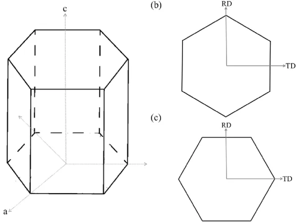
Generally, for simplicity, the crystal coordinate system is set based on the crystal symmetry. For instance, in the case of a cubic crystal structure, an orthogonal frame with [100] , [010] and [001] axes is considered as the crystal frame. In the less symmetric crystal structures, e.g. hexagonal close packed (hcp) and trigonal, an orthogonal frame should be associated with the crystal axes, Fig. 2.2(a). In the case of hcp crystal structure, different orthogonal frames can be considered. For instance, two of the commonly used orthogonal frames which follow the SC-CC
relationships presented in Eq. 2.1 and 2.2 are depicted in Fig. 2.2(b,c). RD || [2110]
ND || [0001] 2.1
TD || [2110]
Figure 2.2. (a) The hcp crystal structure and (b,c) frequently used SC-CC overlaps for the hcp
crystal structure are presented.
Based on the relationship between the sample coordinate system and the crystal coordinate system, an orientation can be expressed as the position of the crystal coordinate system with respect to the sample coordinate system, Eq. 2.3,
where CC is the crystal coordinate system, g is the rotation matrix and CS is the sample
coordinate system. Therefore, the rotation matrix can be defined as the rotation required coinciding the crystal coordinate system with the sample reference coordinate system. Since the size of CC and CS matrices are 3*1 (Eq. 2.3), the size of the rotation matrix is 3*3. The cosines of
the angles between the three axes of the sample coordinate system (i.e., X, Y and Z) and the first axis of the crystal coordinate system (i.e., [100]) make the first row of the rotation matrix (Eq.
C S
2.3). The second and the third rows are made similarly by calculating the cosines of the [010] and [001] with the axes of the sample coordinate system, respectively.
1 1 1
2 2 2
3 3 3
cos cos cos
cos cos cos
cos cos cos
g 2.4
The other descriptors of the orientation can be calculated mathematically from the rotation matrix. The relationship between these descriptors and the rotation matrix is shown in Fig. 2.3.
Figure 2.3. Frequently used orientation descriptors which can be calculated from the rotation matrix are presented (adapted from ref. [14]).
It is noteworthy to mention that depending on the number of symmetries associated with the crystal and specimen, it is possible to assign more than one rotation matrix to coincide the crystal coordinate system with the sample coordinate system. For instance, the number of symmetry elements of the cubic and hexagonal crystal structures is 24 and 12, respectively. In other words, the orientation of the hcp crystal structure shown in Fig. 2.2(a), can be represented in 12 symmetrically equivalent ways by 12 different rotation matrices. The rotational symmetry elements for the hcp crystal structure are tabulated in Table 2.1.
The statistical sample symmetry is related directly to the symmetry of the preceding deformation. In general, the sample symmetry reflects the lowest symmetry deformation that was
imposed on a material. For instance, rolling is a plane strain deformation with orthorhombic symmetry, wire drawing as well as uniaxial compression are axisymmetric deformation with cylindrical symmetry and torsion is a simple shear with monoclinic symmetry.
Table 2.1 Rotation symmetries associated with the hcp crystal structure (adapted from ref. [15])
1 0 0 I= 0 1 0 0 0 1 6 1 / 2 3 / 2 0 C = 3 / 2 1 / 2 0 0 0 1 z 3 1 / 2 3 / 2 0 C = 3 / 2 1 / 2 0 0 0 1 z 2 1 0 0 C = 0 1 0 0 0 1 z 6 1 / 2 3 / 2 0 C = 3 / 2 1 / 2 0 0 0 1 z 3 1 / 2 3 / 2 0 C = 3 / 2 1 / 2 0 0 0 1 z 21 1 0 0 C = 0 1 0 0 0 1 22 1 / 2 3 / 2 0 C = 3 / 2 1 / 2 0 0 0 1 23 1 / 2 3 / 2 0 C = 3 / 2 1 / 2 0 0 0 1 21 1 0 0 C = 0 1 0 0 0 1 22 1 / 2 3 / 2 0 C = 3 / 2 1 / 2 0 0 0 1 23 1 / 2 3 / 2 0 C = 3 / 2 1 / 2 0 0 0 1
Pole figure and inverse pole figure 2.1.2.
The normal direction to a crystal plane can be represented as a point on the unit reference sphere which surrounds the crystal, Fig. 2.4. The crystallographic orientation of the crystal presented in this figure can be shown with respect to an external frame based on the values of and angles. Remarkably, the complete orientation of the crystal cannot be specified only by one pole due to the fact that the crystal can be rotated about the crystal normal direction while the position of the pole is fixed (i.e., and angles do not change if the crystal is rotated about [001] direction). In general, depending on the symmetry of the crystal structure, two to three different poles are required to determine the exact orientation of a crystal/lattice. Pole figure
plots which are the derivatives of stereographic projections are used frequently in orientation microscopy analyses. A pole figure indicates the position of a pole (a perpendicular direction to a lattice plane) with respect to the sample reference frame. In other words, the reference coordinate system of a pole figure is the sample reference frame. An example of plotting a pole figure plot of (100) poles for a cubic crystal is shown in Fig. 2.5(a,b). The angle in Fig. 2.5(b) represents the azimuth of the pole and the angle is the rotation of the pole about the polar axis. In practice, the spatial arrangements of the and angles are set based on the external reference frame which is the sample coordinate system. As an example, in a rolled sample, the sheet normal direction is considered to be the north pole of the sphere (i.e., =0° for the normal direction). Similarly, the rotation angle is set to zero for the reference direction (or the rolling direction) [14].
In contrast to a pole figure, it is possible to show the sample directions with respect to the crystal coordinate system. This type of plot is called an inverse pole figure (IPF). An example of an IPF plot associated with a cubic crystal structure is depicted in Fig. 2.6. In the pole figure plot shown in Fig. 2.6(a), all the symmetrically equivalent poles are presented. The inverse pole figure of the same orientation is depicted in the unit triangle, Fig. 2.6(b). In this plot, the normal direction of the sample is plotted with respect to the crystal axes. The main feature of the unit triangle is showing one point per orientation in the plot. As stated previously, in the case of a cubic crystal structure, each orientation has 24 symmetrically equivalent orientations. Twelve of these orientations are located in the north hemisphere and the rest are located in the south hemisphere.
Figure 2.4. The orientation of (001) plane in a cubic system is shown. The position of (001) pole with respect to an external frame can be found by and angles (adapted from ref. [14]).
Figure 2.5. (a) Representation of {100} poles of a cubic crystal in a unit sphere and (b) {100} pole figure are depicted (adapted from ref. [14]).
Figure 2.6. The pole figure of a cubic crystal structure and (b) the inverse pole figure are presented.
Euler angles 2.1.3.
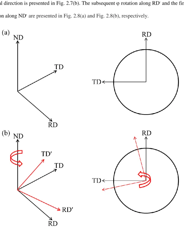
Euler angles are specific types of rotations used in orientation microscopy to transform the sample coordinate system to the crystal coordinate system. Among different conventions used for the Euler angles (e.g. Roe and Kocks), Bunge convention is used commonly. The notations of the Bunge Euler angles are 1,, 2. Based on the Bunge Euler angles, three rotations are
applied in the following sequence [16]:
1. Transforming the rolling direction (RD) to RD and the transverse direction (TD) into TD by 1 rotation about the normal direction (ND)
2. Rotating about RD
3. Rotating2 about ND (notably, ND rotated out of axis in step two. Therefore, in step
three, the rotation should be operated about ND.)
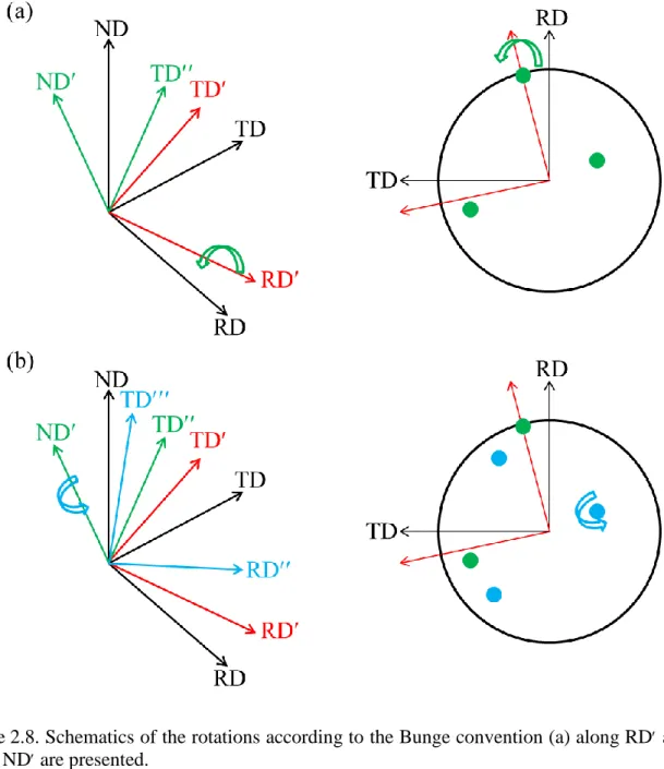
To shed more light on this subject, all the rotation steps are presented in Fig. 2.7 and Fig. 2.8. In Fig. 2.7(a), the sample coordinate system is presented. Applying 1 rotation along the
normal direction is presented in Fig. 2.7(b). The subsequent rotation along RDand the final 2
rotation along ND are presented in Fig. 2.8(a) and Fig. 2.8(b), respectively.
Figure 2.7. (a) The sample frame and (b) rotation along ND according to the Bunge Euler angle convention are presented.
Figure 2.8. Schematics of the rotations according to the Bunge convention (a) along RD and (b) along ND are presented.
Mathematically, these rotations can be represented as matrices which are expressed in Eq. 2.5, Eq. 2.6 and Eq. 2.7. The rotation matrix g can be correlated to the three Bunge Euler angles by the multiplications of these three matrices in order, Eq. 2.8.
1 1 1 φ 1 1 cosφ sinφ 0 sinφ cosφ 0 0 0 1 g 2.5 φ 1 0 0 0 cosφ sinφ 0 sinφ cosφ g 2.6 2 2 φ 2 2 cosφ sinφ 0 sinφ cosφ 0 0 0 1 2 g 2.7 1 φ * φ* φ 2 g g g g 2.8
As expected, all the Bunge Euler angles are periodic with period 2. Moreover, since there is a glide plane in the Euler space, a reflection in the plane = exists. Also, a simultaneous displacement exists through in 1 and 2[14]. Therefore, the domains of the three Bunge Euler
angles are defined according to Eq. 2.9, Eq. 2.10 and Eq. 2.11.
Notably, the range of the Bunge Euler angle domains is affected by the sample and crystal symmetries. The domain of the first Bunge Euler angle (i.e.,1) is affected by the sample
symmetries. For instance, in the case in which the sample has no symmetry (also called triclinic symmetry), the domain of 1 angle is defined in the range pointed out in Eq. 2.9. However, in the
rolled sample in which two mirrors can be considered in the rolling and transverse directions (i.e., orthonormal sample symmetry), the domain of the 1 angle is defined according to Eq. 2.12.
1 0 φ 360 2.9 0 φ 180 2.10 2 0 φ 360 2.11 1 0 φ 90 2.12
Crystal symmetries affect the range of and 2 angles. Generally speaking, an n-fold
symmetry axis limits the 2 domain within 0° and 360°/n. The existence of mirror planes or an
additional two-fold symmetry reduces the domain from 180° to 90°.
Angle/axis of rotation and misorientation 2.1.4.
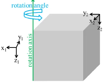
It is pointed out in section 2.1.3 that by three consecutive rotations, it is possible to coincide the crystal coordinate system with the sample coordinate system. Another way of achieving this overlapping of the mentioned coordinate systems is applying a rotation angle along a specific rotation axis. As shown in Fig. 2.9, it is possible to overlap the coordinate system x1y1z1 to
coordinate system x2y2z2 by rotating the first coordinate system along the rotation axis for a
specific rotation angle. This combination is called an angle/axis pair. In a case of overlapping a sample coordinate system (sample frame) to a crystal coordinate system (crystal frame), the mentioned pair is called an angle/axis of rotation while if the overlapping is between two crystal coordinate systems, the pair is called an angle/axis of misorientation. The misorientation between two crystals (orientations) can be calculated according to Eq. 2.13,
where g is the rotation matrix. The angle and axis of misorientation can be determined readily following Eq. 2.14 and Eq. 2.15, respectively.
-1 12 1 2 M g g 2.13 11 22 33 (M M M 1) cos θ 2 2.14 23 32 1 31 13 2 12 21 3 (M -M ) r 2sin(θ) (M -M ) r 2sin(θ) (M -M ) r 2sin(θ) 2.15
Figure 2.9. A single rotation along the presented rotation axis is required to overlap the x1y1z1
coordinate system on the x2y2z2 coordinate system (adapted from ref. [14]).
An angle/axis of rotation does not provide very useful physical information about the orientation relationship between a crystal frame and a sample frame. In contrast, the angle/axis of misorientation is used widely to study the grain boundaries and crystallographic analyses between adjacent grains/phases.
The Rodrigues space 2.1.5.
Another way of presenting an orientation/misorientation is a 3D vector. Direction and magnitude are two important features of a vector. As mentioned previously, an orientation/misorientation can be presented by a rotation angle along a specific rotation axis. Therefore, it is possible to consider the direction of a vector as the rotation axis and the magnitude of the vector as the rotation angle. This special vector is named the Rodrigues vector
(R). R vector combines the axis and angle of rotation/misorientation into a single mathematical identity as presented in Eq. 2.16,
where is the angle of rotation/misorientation and r is the axis of rotation/misorientation. Since the three components of the R vector lie in a Cartesian coordinate system, each orientation/misorientation can be presented in a 3D space called Rodrigues-Frank (RF) space. The main advantage of the RF space is the representation of an orientation/misorientation in a straight line geometry which makes the visualization of an orientation/misorientation easier. Lines presenting the orientations/misorientations in the RF space are called geodesic lines. Shifting the origin of the RF space does not change these straight lines [17]. Also, the distribution of the random orientations is almost uniform in the RF space.
Fundamental zone 2.1.6.
As stated in section 2.1.1, crystals have different types of symmetries (e.g., 12 symmetry elements for an hcp crystal). The complete RF space of orientation contains all the symmetrically equivalent orientations of each orientation (e.g., 12 different representations of the same crystal orientation in the complete RF space). Since it is easier to work with one presentation for each crystal orientation, generally the representation with the smallest rotation angle is chosen. Therefore, all the points (end points of the R vectors) are surrounded by a polyhedron called the fundamental zone of the RF space. Hence, by applying symmetries to an orientation located outside of the fundamental zone, it is possible to find the symmetrically equivalent point inside the fundamental zone. The shape of the complete orientation space (considering no symmetry element), the fundamental zone of orientation associated with the hcp crystal structure and the fundamental zone of misorientation associated with the hcp/hcp are presented in Fig. 2.10. For
θ =tan 2 R .r 2.16
the sake of completeness, the fundamental zone of the cubic crystal system has six octagonal faces perpendicular to the four-fold axes and eight triangular faces perpendicular to the three-fold axes. It occupies 1/48 of the total space and the distance of the origin from the main face is tan (/8). Similarly, the fundamental zone of the hexagonal crystal system has two dodecagonal faces perpendicular to the six-fold axis and twelve square faces perpendicular to the diad axes. It occupies 1/12 of the total space and the distance of the origin from the main face is tan (/4) [18].
Figure 2.10. The complete orientation space (triclinic orientation fundamental zone), hcp orientation fundamental zone and the hcp/hcp misorientation fundamental zone are presented in gray, blue and green colors, respectively.
2.2. Orientation Microscopy Techniques
Micro-Kossel technique 2.2.1.
X-ray diffraction at the crystal lattice due to the interaction of an electron beam with a sample makes the basis of the Micro-Kossel technique. This technique has been used to determine the local orientation in scanning electron microscopes (SEM) [19, 20]. X-radiation is reflected at the lattice planes associated with the sample following Braggs law. Since these planes are irradiated from all directions, cone-shaped planes with a half apex angle 90°- are formed by the reflected x-rays. These cones are called Kossel cones, Fig. 2.11.
Figure 2.11. The schematic of Kossel pattern formation in reflection condition is presented (adapted from ref. [14]).
The wavelength of the x-rays formed in this technique is remarkably large. As presented in Fig. 2.12, the large wavelength results in curvy projection lines due to satisfying a large interval of Bragg angles (e.g., 0° to 90°).
Figure 2.12. A Kossel pattern of titanium is shown (Courtesy of F. Friedel).
The spatial resolution of this technique is ~10 m in reflection [20] and ~20 m in transmission [21] which limits its application to the characterization of coarse grains. Also, the signal-to-noise ratio of Kossel patterns is considerably large which makes their analyses difficult. Due to these limitations, the application of this technique is limited to the characterization of unknown crystal structures [22] and the quantification of internal stresses [23].
Kikuchi diffraction pattern 2.2.2.
Selected area channeling (SAC) and electron backscatter diffraction (EBSD) in SEM as well as convergent beam electron diffraction (CBED) in TEM are the frequently used electron diffraction techniques which are based on Kikuchi diffraction patterns [24-26].
2.2.2.1 Formation of Kikuchi patterns
The interaction of an electron beam with a sample scatters the beam diffusely in all directions. For each set of lattice planes, it is expected that some electrons are arriving at the Bragg angle (B) and undergo elastic scattering. Therefore, as a result of the interaction of an
electron beam with different lattice planes, reinforced strong diffracted beams form, Fig. 2.13.
Figure 2.13. Scattered electrons which satisfy the Bragg angle condition are diffracted (adapted from ref. [27]).
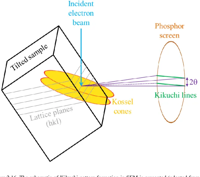
Since the diffraction at the Bragg angle condition is occurring in all directions, the diffracted radiation forms a surface of a cone (called Kossel cone). Considering the source of electrons which are scattering to be located between the lattice planes, the formation of two radiation cones is expected, Fig. 2.14.
Figure 2.14. A schematic of Kikuchi pattern formation in TEM is presented. The diffracted electrons form Kossel cones at point P located at the hkl planes (adapted from ref. [27]).
These cones extend around the perpendicular direction of the reflecting atomic planes with 90°-B. Since the electron wavelength is small, the Bragg angles are also small according to Eq.
2.17,
where is the electron wavelength and d is the distance between two hkl planes. Therefore, the cones are almost flat and their projection on a screen is expected to form conic sections which resemble pairs of straight, parallel lines. These parallel lines are called Kikuchi lines and the distance between the two lines of each pair (band) represents the angular distance of 2B.
Therefore, each band has a specific width which can be assigned to a specific crystallographic plane. Also, the intersection of these bands forms a zone axis, Fig. 2.15. A Kikuchi pattern reflects symmetries existing in a crystal structure through representing all the angular relationships between different diffracting planes of the crystal. Noteworthy, the Kikuchi pattern formation shown in Fig. 2.14 belongs to the TEM diffraction condition. Kikuchi pattern formation in SEM is depicted in Fig. 2.16. The Kikuchi lines formed in TEM are sharper than SEM.
Figure 2.15. The intersection of several bands forms a zone axis. The zone axis is surrounded by a red circle is this figure.
hkl B
Figure 2.16. The schematic of Kikuchi pattern formation in SEM is presented (adapted from ref. [14]).
Depending on where the detector is installed in a SEM instrument, the sample can be either tilted for 70° from the horizontal line or it can be at a zero tilt condition [28]. The former is generally called electron backscatter diffraction (EBSD) [29-31] and the latter is called transmission Kikuchi diffraction (TKD) or transmission EBSD (t-EBSD) [32-34].
At the end, it should be noted that in the case of selected area channeling (SAC) in which the incident beam is rocking at the sample site, the band formation mechanism is slightly different from the one pointed out in this section. In the SAC case, the band formation mechanism is
called pseudo-Kikuchi bands. However, bands formed in the SAC method provide the same geometry and crystallographic information which can be derived from Kikuchi patterns.
2.2.2.2 Qualitative information extracted from Kikuchi patterns
Important information can be extracted by visual evaluations of the Kikuchi patterns. For instance, the location of grain boundaries as well as lattice strain can be assessed qualitatively as follows:
Grain boundary/interface detection:
Grain boundaries can be detected by comparing the quality of the acquired diffraction patterns at different locations of a sample. The Kikuchi patterns at the grain boundaries are less sharp in comparison to an area located inside the grains. The main reason for the reduction of the diffraction pattern quality can be assigned to the overlap of diffraction patterns formed from both sides of the grain boundary due to the fact that the interaction volume of the incident electron beam partially penetrates to the two grains located adjacent to each grain boundary side. The reduction of the sharpness of the diffraction pattern close to the grain boundary is shown nicely in Fig. 2.17 for an iron bicrystal sample using the EBSD technique [11].
Figure 2.17. Recorded Kikuchi patterns associated with different distances from the grain boundary in an iron bicrystal are presented. The acquired diffraction patterns are sharper in areas located far from the grain boundaries (e.g., cases 1 and 8) in comparison with case 4 which is located adjacent to the grain boundary [11].
Qualitative elastic strain determination:
The lattice of a crystal is distorted by the presence of elastic strain. The elastic strain degrades the quality of the acquired diffraction patterns. This degradation is considerable in the cases in which crystals are bent [35]. The reduction in the quality of a bent crystal in comparison to an unstrained crystal is shown in Fig. 2.18. The degradation is due to the slight deviation from the Bragg angle along the length of the planes which results in less sharp recorded Kikuchi diffraction patterns [36]. Notably, in the cases in which the strain does not make any bending (e.g., uniaxial strain along a principle direction of a unit cell), the width of some diffraction bands as well as the location of some zone axes change [37].
Figure 2.18. Bending a crystal reduces the quality of the recorded diffraction patterns. The schematics of (a) an unstrained crystal and its associated Kikuchi diffraction pattern and (b) a bent crystal and its Kikuchi diffraction pattern are presented [35].
2.2.2.3 Quantitative information extracted from Kikuchi patterns
In addition to the qualitative assessment of the Kikuchi patterns, it is possible to extract quantitative information such as evaluations of the stored energy due to the presence of residual elastic strain, crystal orientation determination and elastic strain measurements.
Evaluations of the stored energy due to the presence of residual elastic strain:
Since the presence of elastic strain gradient distorts the crystal lattice, the sharpness of the Kikuchi bands degrades [38]. The sharpness variation of the Kikuchi bands is the basis of image quality map formation in EBSD. Based on the mentioned relationship between the elastic strain gradient and the relative difference of the image quality values, it is possible to make a correlation between the stored energy due to the presence of residual strain and image quality values [39]. The relative stored energy can be determined from the image quality values following Eq. 2.18,
where H is the relative stored energy for a point in arbitrary units, IQ is the image quality value for that point, IQmax is the maximum value of the image quality for all the studied points and f as
well as K factors are constants which determine the lower and upper limits of the stored energy max
IQ
H=k(1- )
distribution. An example of the stored energy distribution is given in Fig. 2.19 for a 60% cold-rolled commercially pure titanium alloy [39].
Figure 2.19. The stored energy distribution for a largely deformed commercially pure titanium alloy obtained by EBSD is presented [39].
Crystal orientation determination:
To determine the crystal orientation, the acquired Kikuchi patterns are post processed in two steps. Initially, the Kikuchi pattern is indexed (i.e., determination of the crystallographic indices of the poles and bands) and then the relative positions of the poles and bands are determined with respect to the sample reference frame. In order to index a recorded Kikuchi pattern image, primarily, some image processing algorithms are applied to increase the possibility of detecting Kikuchi bands. These image processing algorithms are applied to subtract the background of the recorded diffraction pattern and improve the contrast of the acquired image. For instance, Burns algorithm (which is used to detect straight lines) [40] has been used to distinguish edges of the
Kikuchi bands from the local intensity gradient [31]. However, these days depending on the software used for indexing the Kikuchi patterns, a wide range of image processing algorithms are used to distinguish Kikuchi bands from the rest of the recorded image. To accelerate the indexing procedure and also improve the signal to noise ratio by a local integration of the pixel intensities, the size of the recorded image is reduced. In the next step, Hough transformation is applied to the images [30, 41]. In this type of transformation, each point with the coordinate of xi and yi in the
image is transformed to a sinusoidal curve in Hough space which is an accumulation space. This transformation is done according to Eq. 2.19,
where and are axes of the Hough space and they vary from –R to R and 0° to 180°, respectively. Notably, to reduce the shading effect in the Hough transformed image, only a circle with the diameter of 2R is selected from the square-shape recorded diffraction pattern. An example of applying Hough transformation to a line is shown in Fig. 2.20. Points selected on the line presented in Fig. 2.20(a) are converted to sinusoidal curves in the Hough space, Fig. 2.20(b). All these curves intersect at a specific point which represents the straight line shown in Fig. 2.20(a). As mentioned previously, some image processing algorithms are applied to gray scale recorded Kikuchi pattern images to distinguish points located at the edges of the Kikuchi bands. Considering the intensity of the points improves the line detection by the Hough transform method.
The next step is finding peaks in the Hough transformed image. The detected peaks represent the edges of the Kikuchi bands in a recorded diffraction image. The angles between the detected lines are measured. These angles are compared with the interplanar angles of the studied material which can be made from X-ray powder diffraction results as well as kinematical
i i
Figure 2.20. (a) A straight line and (b) the corresponding Hough transformed curves of the points shown in (a) are presented (adapted from ref. [14]).
calculations based on the space group symmetry and the locations of atoms in a unit cell [42]. One of the methods to match the detected angles with the calculated values is the triplet method. In this method, a set of three bands are selected and the angles made between these bands are compared with the calculated values [43]. Each triplet set may satisfy more than one orientation solution. To find the best solution for each triplet, all the solutions receive votes. The solution which obtains the highest number of votes is considered as the most probable solution for the recorded diffraction pattern image. Some parameters are defined to assess the quality of indexing. For instance, confidence index (CI) [44] which represents the difference between the first and second solutions with the highest number of votes is used frequently. This parameter is calculated according to Eq. 2.20,
where V1 and V2are the first and second solutions and t is the number of triplets which can be calculated from the number of bands (i.e., n) following Eq. 2.21,
Another criterion which can be used to differentiate solutions is called fit parameter. This parameter indicates the average angular deviation of the detected Kikuchi bands in the recorded image with respect to the reconstructed bands generated from the orientation solutions [45]. Notably, increasing the number of triplets improves the reliability of the indexing procedure. The complete indexing procedure is shown nicely in Fig. 2.21.
V V CI= t 1 2 2.20 n! t= 3!*(n-3)! 2.21
Figure 2.21. A schematic of the crystal orientation determination from a recorded diffraction pattern image is presented (adapted from ref. [46]).
The spatial resolution of the EBSD technique installed on a scanning electron microscope operating by a field emission gun is ~30 nm along the tilt axis [10] and ~90 nm perpendicular to the tilt axis [11]. This spatial resolution belongs to the EBSD detector configuration in which the sample is required to be tilted to 70° from the horizontal line. Noteworthy, the spatial resolution changes as a function of deformation, the atomic number of a studied material, etc. As an example, the spatial resolution of light atomic density materials (e.g., magnesium) is low.
Recently, a new configuration has been used for orientation microscopy using SEM. In this configuration, the EBSD detector is located under the sample at the zero tilt condition. This new technique is called transmission EBSD (t-EBSD) [33]. Clearly, in contrast to the EBSD technique, an electron transparent sample is required in the t-EBSD technique. The spatial resolution of t-EBSD is claimed to be 10 nm [34]. The spatial resolution of the EBSD technique was improved to 10 nm by reducing the accelerating voltage to 7.5 keV. However, the signal-to-noise ratio dramatically reduces due to the reduction in the accelerating voltage. Also, this method cannot be applied readily to the current EBSD equipment and the standard set-up [47]. The probability of success for this type of experiment highly depends on the phosphor screen. A potential breakthrough to fix these problems is the direct detection of the electron backscatter diffraction patterns by a complementary metal-oxide-semiconductor sensor. Using this sensor provides sharper bands in the acquired diffraction pattern images, a considerable improvement in the signal-to-noise ratio and a high spatial resolution. Also, the angular resolution may improve by using this sensor at the beam energy values below which conventional indirect detectors are not functional [48]. Notably, the angular resolution of EBSD systems in which Hough transform and a look-up table of interplanar angles are used for indexing is ~0.5° [49] to ~2° [50]. The sensitivity of the relative misorientation for 2° angular resolution is ~0.5° [51]. However, analyses of the Kikuchi patterns using image correlation methods improve the sensitivity of the lattice misorientation determination up to 0.006° [52]. This type of Kikuchi pattern analysis provides the basis of the high resolution electron backscatter diffraction (HR-EBSD) technique. In this technique, infinitesimal small deformation theory is used to calculate the lattice rotations and elastic strain from the small shifts in the Kikuchi pattern images [53]. As stated previously, the lattice plane spacing as well as the angle between different planes vary as a function of the
elastic strain changes. The Kikuchi patterns shift as a result of this elastic strain variation. Also, for the sake of completeness, notable improvements in the angular resolution of SEM-based EBSD orientation datasets have been reported using other computational methods. In other words, these methods apply different ways of noise reduction in the orientation datasets and improvements in smoothing the inverse pole figure maps while preserving the boundaries [54, 55]. One of the methods of improving the angular resolution is using quaternion averaging which averages the misorientation between two data points. For instance, the Kuwahara filter [54] allows for a pixel (one orientation set) to adopt the average orientation of a region surrounding the pixel. Notably, this method of improving the angular resolution of SEM-based orientation studies was not suggested to be used for severely deformed materials in which large misorientation gradients exist [54]. A large misorientation gradient between two neighboring pixels cannot be avoided due to the fact that the spatial resolution of EBSD is ~90 nm [11].
Elastic strain measurements:
In the HR-EBSD technique, the displacement gradient tensor is extracted from the cross correlation of two or more diffraction pattern images. One of the diffraction patterns is considered as the reference and the others are called the test patterns. Initially, the images are transformed to the Fourier domain by a two-dimension fast Fourier transform (FFT). The transformed images are filtered to reduce the low frequency background gradients and high frequency noise. The normalized cross correlation is calculated for the reference diffraction pattern and the test patterns, Fig. 2.22.
Figure 2.22. Shifts in x and y directions of the test pattern with respect to the reference pattern are calculated using a cross correlation function [53].
Based on the location of the cross correlation peak, it is possible to determine the required shifts in x and y directions to make the maximum match between the reference pattern and each test diffraction pattern. The relationship between the displacement gradient tensor and the calculated diffraction pattern shifts can be shown as follow.
The displacement gradient tensor which indicates the small strain and rotations between two crystals can be described according to Eq. 2.22,
1 1 1 1 2 3 2 2 2 1 2 3 3 3 3 1 2 3 u u u x x x u u u x x x u u u x x x A I 2.22
where I is the identity matrix, xi and ui are a direction in the crystal and a displacement in the ith
direction, respectively. This tensor shows a relationship between an arbitrary direction (r) in a reference crystal with respect to the deformed crystal (i.e., r direction). It is remarkable to note that since the diffraction patterns are recorded on a phosphor screen, shifts are measured as a projection of Q which is perpendicular to r, Fig. 2.23, and results in the use of the vector q
according to Eq. 2.23,
where is an unknown scalar.
Figure 2.23. Zone axis shifts between a strained crystal (green) and a reference frame (blue) are shown (adapted from ref. [53, 56]).
By measuring the shifts at four different locations of a diffraction pattern, eight components of the displacement gradient tensor can be calculated according to Eq. 2.24 and Eq. 2.25. Doing
λ { (λ 1) }
some mathematical calculations, it is possible to show a relationship between the displacement gradient tensor and diffraction shifts (i.e., Q) at a specific location of the reference sample (i.e.,
r) according to Eq. 2.26 and Eq. 2.27. The lattice rotation and elastic strain values are calculated from anti-symmetric and symmetric components of the displacement gradient tensor [53].
2.3. Orientation Microscopy Using ASTAR/Precession Electron Diffraction (ASTAR/PED) Method
Orientation mapping using a transmission electron microscope (TEM) has been done using different techniques such as conical dark field scanning imaging and transmitted Kikuchi line pattern recognition [14]. However, the limitations of these techniques hinder their wide applications in orientation microscopy. For instance, transmitted Kikuchi line pattern recognition is highly sensitive to the thickness of the foil and to the density of crystal defects. Dark field scanning imaging is also limited due to the facts that this technique is very time consuming and the dynamical diffraction phenomenon considerably affects the acquired results [57]. Precession assisted crystal orientation mapping (PACOM) – commercially, ASTAR – is an emerging orientation microscopy technique using TEM [58]. In this technique, the step size can be as small as 2-5 nm [12, 13] due to the ~1 nm diameter of the direct beam of TEM [59]. The spatial
2 2 3 3 3 1 1 1 1 3 2 3 3 1 2 1 3 1 1 3 1 3 2 3 1 2 u u u u u u r r r r r r r r r q r q x x x x x x 2.24 2 2 3 3 3 2 2 2 2 3 1 3 3 1 2 2 3 2 2 3 2 3 1 3 1 2 u u u u u u r r r r r r r r r q r q x x x x x x 2.25 2 3 3 3 1 1 1 1 2 1 1 2 3 1 1 3 2 3 3 1 3 2 u u u u u u r r r r r r Q x x x x r x r x 2.26 2 3 3 3 2 2 2 1 2 2 2 1 3 2 2 3 1 3 3 1 3 2 u u u u u u r r r r r r Q x x x x r x r x 2.27
resolution of this technique depends on the focused beam size and the scanning step size. The beam size is affected by the condenser aperture as well as the precession angle which broadens the beam due to the spherical aberration of TEM for nonaxial trajectories [13]. An example of the beam broadening curve for a field emission gun type of a 200 keV TEM and a condenser aperture size of 10 m is shown in Fig. 2.24. Interestingly, in a case in which the direct beam is not precessed, the intensities of the excited reflections are not correlated to the square of the structure factor. However, increasing the precession angle reduces the deviation at the expense of the spatial resolution (due to beam broadening) [60].
Figure 2.24. Beam broadening as a function of precession angle is shown. The vertical axis is the beam diameter and the horizontal axis is the precession angle. (a), (b) and (c) represent the projections of the beam on the TEM fluorescent screen [13].
The terminology of ASTAR/PED is selected for the technique used in the current study. The first term (i.e., ASTAR) represents the technology (i.e., hardware and software package)
used to scan the sample by rastering the direct beam. The second term (i.e., PED) is related to the coils which precess the direct beam from the optic axis. It is important to mention that D-STEM/PED [61], PACOM [13], IFPOM [62] and ACOM-TEM [63] are alternative terminologies used for the ASTAR/PED technique in the literature.
Precessing the direct beam of TEM forms a cone. The pivot point of this cone is located on the foil. A hollow-circle array of diffraction spots is generated when the incident beam exits the foil. Applying a counter precession signal at the back focal plane of the objective lens makes a pseudo-static diffraction image [64]. Precessing the direct beam changes the diffraction condition from the dynamical diffraction condition to a quasi-kinematical diffraction condition [65, 66] by integrating the intensity of the diffraction spots over a large interval of the deviation parameter [57]. In the dynamical condition, the diffraction patterns suffer from a high level of background intensity with respect to the diffraction spots, due to the presence of forbidden reflections, double diffractions or channeling, integration of the direct and diffracted beams as well as multiple diffraction events. In the quasi-kinematical condition, the diffraction events are integrated, forbidden reflections are eliminated, 180° rotation problem is solved [60] and the background intensity level is far smaller than the intensity of the diffraction spots. Also, precessing the direct beam improves the accuracy of indexing due to the fact that rocking the Ewald sphere in the reciprocal space (which is equivalent to precessing the direct beam in the real space) results in cutting higher order Laue zones in addition to the zero order Laue zone [67].
The effect of precessing the electron beam on improving the quality of the recorded diffraction pattern images is presented in Fig. 2.25. Diffraction patterns associated with a single grain within a thin film of a commercially pure titanium alloy and oriented close to a major zone axis were acquired without precessing the incident beam, Fig. 2.25(a), and with precessing the
direct beam, Fig. 2.25(b). A similar approach was followed for a grain oriented far from a major zone axis, Fig. 2.25(c,d).
Figure 2.25. The contribution of precessing the electron beam on sharpening the recorded diffraction pattern images is presented. (a) The diffraction pattern of a crystal oriented close to 2110 zone axis when the electron beam is not precessed (“PED off” condition) and (b) the same situation as “a” with precessing the direct beam for 1.3° are shown. (c) The diffraction pattern of a crystal oriented far from 0001 zone axis in a PED off condition and (d) the same situation as “c” with PED on condition are depicted [68].
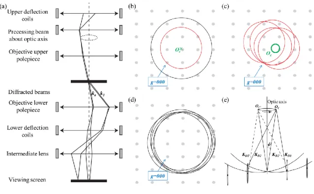
The schematic of the theory of precession electron diffraction is presented in Fig. 2.26(a-e). While the deviation from the ideal Bragg condition and the precession angles are small, these angles are far larger in Fig. 2.26(a-e) for the visualization purposes. As shown in Fig. 2.26(a), the beam is taken off-axis (precessed about the optic axis) for about 0.5°-3.0° using the upper
deflection (beam tilt) coils. The upper pole piece converges the tilted beam to a focused probe at the specimen. In the diffraction mode, the results of the interaction of the precessed beam with the thin foil are the precessed direct beam which passed the sample and the diffracted beams (only one of the diffracted beams is shown in Fig. 2.26(a)). To make the diffraction pattern focused, the lower deflection (beam tilt) coils are used to descan the post-specimen precession. The intersection of the Ewald sphere with the reciprocal lattice is shown in Fig. 2.26(b). The red circle is where the Ewald sphere intersects with the lattice plane while the black circle circumscribes the points that might be visible due to the presence of the rel-rods (reciprocal lattice rods). The projection of the center of the Ewald sphere is shown by Oc (g=000 is the direct
or transmitted beam). Since the direct beam is precessed (Oc is presented as a circle and no
longer as a point) and the Ewald sphere is rocked, Fig. 2.26(c-e), the intersection of the Ewald sphere with the lattice (red circles, Fig. 2.26(c)), especially both its orientation and size will change while remaining fixed to the direct beam. In contrast, the region of diffracted intensities which are the result of the interaction of the Ewald sphere with the rel-rods has a series of overlapping circles, Fig. 2.26(d). The side view of the rocking along the optic axis is shown in Fig. 2.26(e) [12]. Examples of spot diffraction patterns formed by the ASTAR/PED technique are presented in Fig. 2.27(a-c).
To compare the EBSD technique with the ASTAR/PED technique, it should be noted that the scanned area in the ASTAR/PED technique cannot be larger than 15 m*15 m [13] while in the EBSD technique far larger areas can be scanned. Image acquisition speed in ASTAR/PED is about 50 to 200 images per second while the image acquisition speed in EBSD is about 1 to 25 images per second [69]. The indexing of the recorded diffraction pattern images
is offline and online for ASTAR/PED and EBSD techniques, respectively. Also, in terms of the angular
Figure 2.26. Schematics of the precession electron diffraction method are presented with angles which are exaggerated for the visualization purposes. (a) Ray diagram, (b) the original intersection (red circle) of the Ewald sphere with the reciprocal lattice and slice through reciprocal lattice rods (gray circle) without precession (Oc is the projection of the center of the
Ewald sphere), (c) the intersection of the Ewald sphere with the lattice in the rocked condition (precessing the direct beam) where Oc is the projection of the precessing center of the Ewald
sphere, (d) the slide through reciprocal lattice as the beam precesses and (e) side view of the rocking of the Ewald sphere (precessed beam) where Oc is the precessing center of the Ewald
sphere are presented [12].
Figure 2.27. Three examples of the recorded diffraction patterns of an ultrafine grained titanium specimen using NanoMEGAS system are shown [12].
![Figure 2.19. The stored energy distribution for a largely deformed commercially pure titanium alloy obtained by EBSD is presented [39]](https://thumb-us.123doks.com/thumbv2/123dok_us/1409453.2688640/41.918.286.687.198.595/figure-distribution-largely-deformed-commercially-titanium-obtained-presented.webp)

![Figure 2.28. The schematic of formation and accumulation of geometrically necessary edge dislocations is illustrated [96]](https://thumb-us.123doks.com/thumbv2/123dok_us/1409453.2688640/59.918.245.698.420.950/figure-schematic-formation-accumulation-geometrically-necessary-dislocations-illustrated.webp)