http://www.asminternational.org/web/edfas/news/edfa/-/journal_content/56/10192/25602512/MAGAZINE
Copyright 2015 ASM International.
This paper was published in Electronic Device Failure Analysis, Vol. 17, Issue 3, pp. 4-6, 8-10 and is
made available as an electronic reprint with the permission of ASM International.
One print or electronic copy may be made for personal use only. Systematic or multiple
reproduction, distribution to multiple locations via electronic or other means, duplications of any
material in this paper for a fee or for commercial purposes, or modification of the content of this
paper are prohibited.
ELEC TR ON IC DEVIC E F AIL URE AN AL YSIS | VOL UME 1 7 N O. 3
F
or more than a decade, the atomic force microscope(AFM) has been a cornerstone for nanoprobing
integrated circuits, due its precise force control, nanometer-scale resolution, and nondestructive nature.[1]
New capabilities, such as scanning conductance, scanning capacitance, pulsed current-voltage measurement, and capacitance-voltage spectroscopy, have been widely adopted by the integrated circuit analysis community.
Many new techniques continue to be developed, and this article presents two techniques: diamond milling and
electrostatic force microscopy.
DIAMOND MILLING WITH AN AFM
Preparation of integrated circuits for nanoprobing typically involves the global delayering of a die with
mechanical polishing to the desired layer. Dimpling
and computer numerical control milling tools have also
been employed to more locally delayer (typically at the millimeter scale). However, these methods become
more time-consuming, risky, and challenging as layer
thicknesses decrease. One such challenge is the require -ment to provide a surface for nanoprobing that is clean, conductive, and at the desired level. Another challenge is
the requirement to provide a large area for nanoprobing at the appropriate level, because different regions often polish at different rates. In early technology nodes, levels
tended to be etch-selective and self-planarized on metal or dielectric layers. Thus, the integrated circuit could
be delayered uniformly to any desired level. However, for advanced technologies, it is increasingly difficult to
provide all of these properties in one process.
As a surface electrical failure analysis technique,
nanoprobing can be performed on either a single
intercon-nect layer or a sequence of multiple interconintercon-nect layers,
with delayering steps in between. If front-end devices are suspected and back-end metal defects can be ruled
out, a single sample-preparation step and subsequent
nanoprobing can usually achieve high levels of success.
However, it is often necessary to check the intercon -nect layer by layer with nanoprobing to verify if a defect
(open or short) is still present. In the past, this type of job required removal of the integrated circuit from the
nanoprobing tool, removal of a metal layer, and
place-ment of the modified integrated circuit back in the tool for another round of nanoprobing. When an analysis must sequentially nanoprobe four to ten layers of metal, the
turnaround time and success rate of the analysis becomes problematic.
For site-specific delayering, failure analysts often
use focused ion beam (FIB) milling, as an alternative to mechanical delayering techniques. In the case of
layer-by-layer analysis, the FIB is used to either open a window
or cut traces to isolate defects. While this may be effective
in the case of gross defects, changes in electrical
charac-teristics are often associated with the FIB milling process
itself, instead of the removal of the defective layer. Focused
ion beam milling with a gallium beam significantly alters subsequent electrical measurements by charging associ -ated with the high-energy gallium ion impacts, as well
as by introducing significant leakage paths from gallium
EMERGING TECHNIQUES IN
ATOMIC FORCE MICROSCOPY:
DIAMOND MILLING AND ELECTROSTATIC
FORCE MICROSCOPY
Stephen Ippolito, Sean Zumwalt, and Andy Erickson, MultiProbe Group, DCG Systems, Inc.
[email protected]
EDFAAO (2015) 3:4-10 1537-0755/$19.00 ©ASM International
“FOCUSED ION BEAM MILLING WITH
A XENON BEAM WAS RECENTLY
INTRODUCED. IT IS A PROMISING
ALTERNATIVE TO GALLIUM, BUT ITS
CHARGING EFFECTS HAVE YET TO BE
ELEC TR ON IC DEVIC E F AIL URE AN AL YSIS | V OL UME 1 7 N O. 3
deposition and implantation. Thus, during critical device
probing, it is difficult to rule out whether an electrically
measured defect is intrinsic or caused by the FIB milling process itself. Focused ion beam milling with a xenon beam was recently introduced. It is a promising
alterna-tive to gallium, but its charging effects have yet to be
characterized.
Diamond milling with a nanoprober is a new alterna
-tive for site-specific sample preparation and delayering of integrated circuits. Diamond milling provides in situ,
localized, precision delayering inside of a nanoprobing tool, thereby decreasing the turnaround time for inte-grated circuit analysis. Furthermore, like other mechanical
delayering techniques, it should not alter the electrical characteristics of the integrated circuit. Diamond milling with an AFM was first demonstrated several years ago.[2-4]
This article presents the application of diamond milling
to site-specific delayering of integrated circuits.
A single-crystal, faceted diamond tip and a
retro-reflecting mirror were mounted on the end of an AFM
cantilever to form the probe shown in Fig. 1(a). The diamond had an end radius of approximately 10 nm, as shown in Fig. 1(b). Several experiments were conducted to determine the optimal process for delayering a 1 µm by 1 µm area in a static random access memory region of a 22 nm integrated circuit with the diamond probe from the second metal level to the first metal level. Milling was conducted with a triangle wave (constant velocity) scan
in the forward and reverse direction for each line in the
milled area, as illustrated in Fig. 2(a). A second orthogonal
scan was then conducted on the same area with the fast
and slow axes switched, as illustrated in Fig. 2(b). Finally,
the diamond probe was scanned over the area in constant-force contact mode to sweep the surface of the removed material. Although the integrated circuit is composed of relatively hard materials, these materials are easily cut by the diamond, which is more than an order of magnitude
harder. After a host of trials, the diamond exhibited no significant wear, as expected.
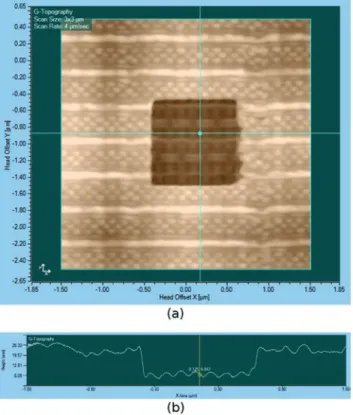
Contact imaging of a 3 µm by 3 µm area, which includes the milling region, is shown in Fig. 3(a). The first metal level is clearly visible in the milled region,
while the second metal level in the surrounding region remains undisturbed. A line cut across the milled region
of the image is shown in Fig. 3(b), which indicates 20 nm of height difference between the metal levels, as well as the generated topography on the first metal level, due to the difference in material-removal rates for the metal and dielectric. In a multiheaded AFM, the sequence of a diamond milling probe and a finer tungsten electrical
probe will provide in situ milling capability for sample preparation and delayering. The diamond milling process
is similar to other mechanical delayering techniques
and therefore is not expected to destructively alter the
Fig. 1 (a) AFM diamond probe with (b) single-crystal, faceted diamond tip
Fig. 2 Diamond milling (a) in first direction, X, and then (b) in second direction, Y
ELEC TR ON IC DEVIC E F AIL URE AN AL YSIS | VOL UME 1 7 N O.
3 electrical characteristics of the integrated circuit. The
authors have also used the diamond probe to mill trenches in silicon as a method of marking cross-sectional scanning capacitance samples. It should be noted that the shape of the diamond tip determines the maximum vertical aspect ratio of diamond-milled trenches.
(continued on page 8)
Fig. 3 Diamond probe delayering of a 22 nm integrated circuit
Fig. 4 Electrostatic force microscopy (a) with a single scanned probe and (b) with a fixed probe added (Active EFM)
ELECTROSTATIC FORCE MICROSCOPY
Electrostatic force microscopy (EFM) is a type of vibrating noncontact AFM in which the force generated by applying an electrical potential difference between an AFM probe tip and a sample is measured.[5,6] The authors
demonstrate that EFM provides capabilities similar to elec
-tron beam absorbed current (EBAC) microscopy without
the associated high-energy electron beam damage.[7,8]
Since the first description and demonstration of EFM, measurements have used only a single AFM probe.[9,10]
Electrostatic force microscopy of integrated circuits was then demonstrated with the additional capability to measure operating circuit potentials.[11,12] As illustrated in
Fig. 4(a), the potential V1 applied to the scanning probe and the potential V2 applied to the substrate result in
intermediate potentials on nanostructures within the
integrated circuit. The applied potential difference typi -cally has both constant and alternating components, to maximize the electrostatic force and its effect on the cantilever resonance.
The capacitance between the AFM probe tip apex
and nearby region of the integrated circuit is an essential
component of the EFM technique. However, parasitic capacitance from the entire integrated circuit to the AFM
probe tip cone and cantilever creates additional measured force.[13] Furthermore, in a delayered integrated circuit, the
nanostructures at or near the surface may have
poten-tials that are less clearly defined, due to junctions and
resistance along multiple paths to the driven substrate potential. Parasitic capacitance and loosely constrained potentials create scanned images with poor signal-to-noise and unclear sources of the resulting potential map.
In the past, these issues have limited the usefulness of EFM as an integrated circuit analysis technique.
Additional AFM probe tips may be introduced to define local boundary conditions on the potential at the nanometer scale, and this technique has been termed “Active EFM.” As illustrated in Fig. 4(b), the potential V3 applied to a second, fixed probe defines the potential on
the nanostructure, which could be a device or metal wire
net. The additional fixed probe tips may or may not be in contact with the integrated circuit, to influence the local
potential of the nanometer-scale structures. This article
presents experimental results of single-probe EFM on an
integrated circuit and then presents the advantages of
selectively biasing individual metal lines in subsequent Active EFM measurements on the same integrated circuit.
Figure 5(a) is a vibrating noncontact AFM topography image of a 4 µm by 4 µm area of an integrated circuit at
(a)
ELEC TR ON IC DEVIC E F AIL URE AN AL YSIS | VOL UME 1 7 N O. 3
the second metal level above the transistors, fabricated
by 22 nm process technology. Figure 5(b) is a single-probe EFM image taken of the same area with the scanning probe
held at a constant height. In the bottom right region of the image, it is possible to discern the metal lines from the dielectric, but the connection paths between metal lines
and the substrate are unclear due to the floating poten
-tials. The upper left region of the image is blurrier due to sample tilt. The first demonstration of the Active EFM technique is shown in Fig. 6(a), with the scanning probe held at constant height and the fixed probe in contact with
a metal line on the surface, thereby driving its potential.
Figure 6(b) is an overlay of the Active EFM signal from
Fig. 6(a) onto the AFM topography image of Fig. 5(a) that indicates the location of the fixed probe and EFM signal
relative to the integrated circuit.
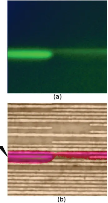
The second demonstration of the Active EFM tech
-nique is shown in Fig. 7(a), with the scanning probe held at constant height and the fixed probe placed in contact
with another metal line on the surface. The second probe drives not only the potential of the surface metal line but also the potential of a subsurface metal line via a circuit interconnection. The faint signal extending
beyond the end of the strong signal in Fig. 7(a) indicates
that a subsurface metal line is electrically connected to the driven surface line. For electrical fault isolation, this has applications for tracing paths associated with driven
potentials, for example, in localizing opens. Figure 7(b)
EMERGING TECHNIQUES IN ATOMIC FORCE MICROSCOPY
(continued from page 6)Fig. 6 (a) Active EFM image and (b) overlay of Active EFM signal onto the topography image
Fig. 5 (a) AFM topography image and (b) single-probe EFM image of a 22 nm integrated circuit
ELEC TR ON IC DEVIC E F AIL URE AN AL YSIS | V OL UME 1 7 N O. 3
is an overlay of the Active EFM signal from Fig. 7(a) onto the AFM topography image of Fig. 5(a) that indicates the location of the fixed probe and EFM signal relative to the integrated circuit. All images in Fig. 5 to 7 were of the same 4 µm by 4 µm area.
In EFM, the force (F) on the scanning probe tip due to the oscillating electric field is proportional to the gradi
-ent in capacitance (C) with height (Z) and the potential difference (V) squared (F ~ (dC/dZ) · V2).[10] The capacitance
gradient between the scanned probe tip and integrated circuit changes as the suspended, scanned probe tip
passes over metal or dielectric, as shown in Fig. 5(b). In the single-probe EFM measurement presented, the sub
-strate is held at a constant potential, V2, and the scanned probe is driven with an alternating potential, V1. In both of the Active EFM measurements presented, the scanned
probe and substrate potentials, V1 and V2, respectively,
were held at ground potential, while constant and
alter-nating potential, V3, was applied to the fixed probe. Thus, in Active EFM, the substrate may be used to guard
the potential of the nanometer-scale structures that are
driven by the fixed probes. In all of the EFM measurements presented, the frequency of the alternating potential was selected to match the frequency of the cantilever reso -nance, thereby driving the oscillation of the cantilever.
A lock-in amplifier was used for synchronous detection of the AFM cantilever displacement amplitude associ -ated with the cantilever oscillation. Thus, the amplitude or phase of the cantilever resonance can be measured
by the same mechanism for non-contact-mode AFM imaging. It should be noted that the fixed probe must be placed outside of the field of view of the scanning probe to prevent mechanical conflict.
SUMMARY
This article has demonstrated that AFM diamond probe
milling is a promising new method for in situ, localized, precision delayering of integrated circuits. It has also
demonstrated that Active EFM can significantly improve
the selectivity of individual circuit nodes relative to
single-probe EFM. Active EFM provides a nondestructive
alternative to EBAC microscopy for localization of opens in integrated circuit analysis.
REFERENCES
1. “Atomic Force Microscopy,” Wikipedia, wikipedia.org/wiki/Atomic_ force_microscopy, accessed Jan. 15, 2015.
2. A. Avdic, A. Lugstein, M. Wu, B. Gollas, I. Pobelov, T. Wandlowski, K. Leonhardt, G. Denuault, and E. Bertagnolli: “Fabrication of Cone-Shaped Boron Doped Diamond and Gold Nanoelectrodes for AFM–SECM,” Nanotechnology, 2011, 22, p. 145306.
3. W. Smirnov, A. Kriele, R. Hoffmann, E. Sillero, J. Hees, O.A. Williams, N. Yang, C. Kranz, and C.E. Nebel: “Diamond-Modified AFM Probes: From Diamond Nanowires to Atomic Force Microscopy-Integrated Boron-Doped Diamond Electrodes,” Anal. Chem., 2011, 83, p. 4936. 4. A. Eifert, W. Smirnov, S. Frittmann, C. Nebel, B. Mizaikoff, and C. Kranz:
“Atomic Force Microscopy Probes with Integrated Boron Doped Diamond Electrodes: Fabrication and Application,” Electrochem. Commun., 2012, 25, p. 30.
5. “Electrostatic Force Microscope,” Wikipedia, wikipedia.org/wiki/ Electrostatic_force_microscope, accessed Jan. 15, 2015.
6. T. Mélin, M. Zdrojek, and D. Brunel: “Electrostatic Force Microscopy and Kelvin Force Microscopy as a Probe of the Electrostatic and Electronic Properties of Carbon Nanotubes,” Scan. Probe Microsc. Nanosci. Nanotechnol., 2010, 4, p. 89.
7. X. Chen, Q. Gao, M. Li, C. Niou, and W.T.K. Chien: “Deformation Study of Low-K Dielectric after E-beam Exposure,” Proc. Int. Symp. Test. Fail. Anal. (ISTFA), 2006, 32, p. 246.
8. K. Dickson, G. Lange, K. Erington, and J. Ybarra: “Electron Beam Absorbed Current as a Means of Locating Metal Defectivity on 45 nm SOI Technology,” Proc. IEEE Int. Symp. Phys. Fail. Anal. Integr. Circuits (IPFA), 2011, 18, p. 1.
Fig. 7 (a) Active EFM image and (b) overlay of Active EFM signal onto the topography image
ELEC TR ON IC DEVIC E F AIL URE AN AL YSIS | VOL UME 1 7 N O. 3
ABOUT THE AUTHORS
Stephen Ippolito has been Chief Technology Officer at Multiprobe for a year. He has worked at Independent Scientific, IBM Semiconductor Research and Development Center, and IBM Thomas J. Watson Research Center during his career in photonics. Dr. Ippolito received a Bachelor of Arts in physics as well as Bachelor and Master of Science degrees in electrical engineering from Boston University in 1999 and a Doctor of Philosophy in electrical engineering in 2004.
Sean Zumwalt has been Director of Applications at Multiprobe for two years. He has been with Multiprobe for over seven years, starting out as an applications engineer. Sean received a Bachelor of Science in physics from the University of California at Santa Barbara in 2007.
Andy Erickson has been Chief Executive Officer at Multiprobe since found
-ing the company in 2001. He has worked at Veeco, Digital Instruments, and Intel
during his career in atomic force microscopy. Andy received a Bachelor of Science in physics from the University of California, San Diego in 1988 and a Master of Science in electrical engineering from the University of Utah in 1995.
9. Y. Martin, C.C. Williams, and H.K. Wickramasinghe: “Atomic Force Microscope—Force Mapping and Profiling on a Sub-100 Å Scale,” J. Appl. Phys., 1987, 61, p. 4723.
10. Y. Martin, D.W. Abraham, and H.K. Wickramasinghe: “High-Resolution Capacitance Measurement and Potentiometry by Force Microscopy,”
Appl. Phys. Lett., 1988, 52, p. 1103.
11. G.E. Bridges, R.A. Said, and D.J. Thompson: “Heterodyne Electrostatic
Force Microscopy for Non-Contact High Frequency Integrated Circuit Measurement,” Electron. Lett., 1993, 29, p. 1448.
12. J.W. Hong, Z.G. Khim, A.S. Hou, and S. Park: “Noninvasive Probing of High Frequency Signal in Integrated Circuits Using Electrostatic Force Microscope,” Rev. Sci. Instrum., 1997, 68, p. 4506.
13. P. Girard, “Electrostatic Force Microscopy: Principles and Some Applications to Semiconductors,” Nanotechnology, 2001, 12, p. 485.
GUEST EDITORIAL
(CONTINUED FROM PAGE 2)
Every so often, system issues point to component-level
problems. Communications and automotive systems
require high power and high bandwidth. We see a lot of standard quad flat no-lead packages, although when
power or bandwidth is stretched, more sophisticated packages are needed to ensure proper transmission
between silicon and system. Such packages require new FA techniques (but not necessarily new tools), especially when observations fall in between silicon scale (nanome
-ter) and bond size (microme-ter)—as exemplified by 2.5-D and 3-D/through-silicon via integration schemes.
Finally, AMRF applications do not require the com
-puting processing needed by advanced CMOS, but they do require high voltage or high speed from alternate materials such as SiGe or III-Vs (e.g., GaAs, GaN, InP).
These devices are not usually challenged in their
capabil-ity to transport rising or falling fronts on time like SOCs
but rather by their parametric capabilities. This leads to analyses wherein relating a failed bin to a device behavior is much more critical than tracing a failed pin down to a
specific transistor.
A pattern has emerged in our FA practice within the
AMRF field. It is no longer how fast we can get into complex
semiconductor devices that really matters but how soon
we can relate an external failure to a faulty behavior—at
the system, package, or component level. Therefore, it is less a matter of having the fastest tool than having the
right knowledge and expertise. Of course, advanced FA tools will continue to be critical for SOC product engineer
-ing and industrialization, predominantly in large IDMs. When it comes to new AMRF applications, legacy tools
can be used with success as long as the right expertise and experience is there to guide their usage and interpret the data they produce.