THE DESIGN, BUILDING, AND TESTING OF A CONSTANT ON DISCREET
JAMMER FOR THE IEEE 802.15.4/ZIGBEE WIRELESS COMMUNICATION
PROTOCOL
A Thesis
presented to
the Faculty of California Polytechnic State University,
San Luis Obispo
In Partial Fulfillment
of the Requirements for the Degree
Master of Science in Electrical Engineering
by
Alexandre Jacques Marette
June 2018
ii
© 2018
Alexandre Jacques Marette
ALL RIGHTS RESERVED
iii
COMMITTEE MEMBERSHIP
TITLE: The Design, Building, and Testing of a
Constant On Discreet Jammer for the IEEE
802.15.4/ZigBee Wireless Communication
Protocol
AUTHOR: Alexandre Jacques Marette
DATE SUBMITTED: June 2018
COMMITTEE CHAIR:
Vladimir Prodanov, Ph.D.
Associate Professor of Electrical Engineering
COMMITTEE MEMBER: Dennis Derickson, Ph.D.
Electrical Engineering Department Chair
COMMITTEE MEMBER:
Bruce DeBruhl, Ph.D.
iv
ABSTRACT
The Design, Building, and Testing of a Constant On Discreet Jammer for the IEEE
802.15.4/ZigBee Wireless Communication Protocol
Alexandre Jacques Marette
As wireless protocols become easier to implement, more products come with wireless
connectivity. This latest push for wireless connectivity has left a gap in the development
of the security and the reliability of some protocols. These wireless protocols can be used
in the growing field of IoT where wireless sensors are used to share information
throughout a network. IoT is being implemented in homes, agriculture, manufactory, and
in the medical field. Disrupting a wireless device from proper communication could
potentially result in production loss, security issues, and bodily harm. The
802.15.4/ZigBee protocol is used in low power, low data rate, and low cost wireless
applications such as medical devices and home automation devices. This protocol uses
CSMA-CA (Carrier Sense Multiple Access w/ Collision Avoidance) which allows for
multiple ZigBee devices to transmit simultaneousness and allows for wireless coexistence
with the existing protocols at the same frequency band. The CSMA-CA MAC layer
seems to introduce an unintentional gap in the reliability of the protocol. By creating a
16-tone signal with center frequencies located in the center of the multiple access
channels, all channels will appear to be in use and the ZigBee device will be unable to
transmit data. The jamming device will be created using the following hardware
implementation. An FPGA connected to a high-speed Digital to Analog Converter will be
used to create a digital signal synthesizer device that will create the 16-tone signal. The
16-tone signal will then be mixed up to the 2.4 GHz band, amplified, and radiated using a
2.4 GHz up-converter device. The transmitted jamming signal will cause the ZigBee
MAC layer to wait indefinitely for the channel to clear. Since the channel will not clear,
the MAC layer will not allow any transmission and the ZigBee devices will not
communicate.
Keywords: IEEE 802.15.4, ZigBee, Jammer, Digital Signal Synthesizer, Software
Defined Radio
v
ACKNOWLEDGMENTS
Firstly, I would like to thank my advisor, Dr. Prodanov, for pushing me to pursue a
challenging project that covers a broad range of electrical engineering topics. His
guidance, knowledge, and motivation in the many topics sampled greatly helped me over
my thesis process.
In addition to my advisor, I would like to thank the additional committee members: Dr.
Derickson and Dr. DeBruhl. Their comments and incites helped refine my thesis report to
ensure an understanding from multiple perspectives.
My sincere thanks go out to the entire Electrical Engineering staff and faculty. Special
thanks to Dr. Zhang, Dr. Danowitz, and Dr. Arakaki whose classes in signals and
systems, digital design, and RF analysis respectively helped me gain the knowledge
necessary to implement many of the special concepts required by this project.
Many thanks go out to my peers and classmates throughout the years. Special thanks to
those who spent late nights in the graduate resource lab working before deadlines, those
who procrastinated with mindless talks and endless coffee runs, and for those who helped
by simply listening to my rants and concerns.
I thank Corey Harris for special contributions to my project in the form of a donated 10
dB coupler and for additional trouble shooting solutions.
Lastly, I would like to thank my family and loved ones: my mom, my sister, my brother,
Emily Whitaker, Ted and Jennifer Worden, Morty Lopez, and Pedro for the immense
support throughout my many years of my academic life. There is no doubt that I would
not be here without these people in my life.
vi
TABLE OF CONTENTSLIST OF FIGURES ... vii
1
INTRODUCTION ... 1
1.1
Statement of Problem ... 1
1.2
IEEE 802.15.4/ZigBee Background ... 2
2
DESIGN OVERVIEW ... 8
2.1
Multi-tone Signal Generation ... 9
2.2
Top Level Overview... 12
2.3
Device Requirements ... 13
3
DIGITAL SYNTHESIZER DESIGN ... 16
3.1
Overview ... 16
3.2
FPGA Design ... 17
3.3
Choosing Parts... 26
3.4
Schematic Design ... 30
3.5
Layout Design ... 39
3.6
Building and Testing ... 46
4
ANALOG UPCONVERTER DESIGN... 56
4.1
Overview ... 56
4.2
Choosing Parts... 56
4.3
Matching Networks ... 60
4.4
Schematic Design ... 69
4.5
Layout Design ... 75
4.6
Building and Testing ... 77
5
SYSTEN TESTING & CHARACTERIZATION ... 87
6
ZIGBEE NETWORK JAMMING ... 91
6.1
Overview ... 91
6.2
Testing Challenges ... 91
6.3
Testing ... 93
6.4
Additional Exploration ... 98
7
CONCLUSION ... 104
7.1
Reflection ... 104
7.2
Future Works ... 105
8
REFERENCES ... 107
9
APPENDICES
APPENDIX A
MATLAB Scripts ... 110
APPENDIX B
Schematics ... 113
APPENDIX C
Layout ... 115
APPENDIX D
Parts List ... 134
vii
LIST OF FIGURES
Figure 1-1: The ZigBee/IEEE 802.15.4 protocol stack [7] ... 3
Figure 1-2:Comparison of different wireless technologies [7] ... 3
Figure 1-3: ZigBee Mesh Network and Device Types [6] ... 4
Figure 1-4: Arrangement of Channels in IEEE 802.15.4 2.4 GHz Band [7] ... 5
Figure 1-5: The Basis slotted CSMA mechanism in IEEE 802.15.4 [7] ... 7
Figure 2-1:16-tone Signal used for complete ZigBee Jamming (top). Multi-tone
Signal used for channel interference in Channels 1-3 while the remaining channels
are left open (bottom)... 8
Figure 2-2: ADS Step Recover Diode Simulation ... 9
Figure 2-3: ADS Simulation of16 Frequency Synthesizers and 15 Couplers with
channels 18 and 19 Disabled... 10
Figure 2-4:MAX2870 32 TQFN Footprint [12] ... 11
Figure 2-5: Early Top-Level Block Diagram... 12
Figure 2-6: Block Diagram with Separate Boards ... 13
Figure 3-1:Early FPGA Block Diagram ... 16
Figure 3-2: First Run FPGA Implementation Results ... 17
Figure 3-3:VQ100 Package Footprint - XC3S200A (Top View) [15] ... 19
Figure 3-4: Spartan 3A FPGA Black Box Diagram ... 20
Figure 3-5: MATLAB Waveform Creator Output for ZigBee at 210 MSPS and
10-bit Words ... 21
Figure 3-6: FPGA Controller FSM Diagram ... 22
Figure 3-7: ISE Design Suite Synthesis Results with XC3S200A ... 24
Figure 3-8: Xilinx iSim FPGA Simulation showing the Data Output in Purple ... 24
Figure 3-9: FPGA iSim Data plotted using MATLAB showing the Time Domain
(top) and the Freq Domain (bottom) ... 25
Figure 3-10: MATLAB DAC Sample and Hold Time Domain (left) and
Frequency Domain (right) ... 25
Figure 3-11: JTAG Configuration Interface [19] ... 28
Figure 3-12: Digital Design Power Estimations ... 29
Figure 3-13: FPGA-DAC Interconnection... 31
Figure 3-14: Digital Synthesizer Switch Banks ... 32
Figure 3-15:JTAG-SMT2 to FPGA connections with Current Limiting
Resistor[20] ... 33
Figure 3-16: Interconnections between the JTAG-SMT2, Reset Switch,
Oscillator, and FPGA ... 33
Figure 3-17:Bypass Capacitor Simulation Schematic (top) and Results (bottom) ... 36
Figure 3-18: AD9740 LC Power Supply Filter [17] ... 36
Figure 3-19 Ferrite Bead Expected Impedance Response (left) and the Impedance
Response from the Simulated Model (right)[22] ... 37
Figure 3-20: LC Filter with Ferrite Bead Simulation Schematic (top) and Results
(bottom)... 38
Figure 3-21: Four-Layer PCB Stack ... 40
Figure 3-22: Digital Synthesizer Layout Plan ... 41
viii
Figure 3-24: Coplanar Wave Guide Trace Width using Saturn PCB Toolkit [23] ... 43
Figure 3-25: AD9740 DAC Layout (right). Digital Synthesizer Ground Plane
Layout (left)[17]... 44
Figure 3-26: Digital Synthesizer Power Plane Layout ... 44
Figure 3-27: Effects of Discontinuities in Ground Plane [21] ... 45
Figure 3-28: Bypass Capacitor Layout for Power and Ground Pins [24] ... 45
Figure 3-29: Bare Digital Synthesizer PCB Board Top (left) & Bottom (right) ... 46
Figure 3-30: Power Supply Load Stability Test ... 48
Figure 3-31: PSRR Test Schematic ... 49
Figure 3-32: Power Supply PSRR Results: Digital 3.3 V (left) Analog 3.3 V
(right) ... 49
Figure 3-33: FSM State Test ... 51
Figure 3-34: DAC Output with Sink Roll-Off View (left) and Close View 0-100
MHz (right) ... 51
Figure 3-35: Differential to Single Power Schematic ... 52
Figure 3-36: DAC Output Single Tone Power ... 53
Figure 3-37: DAC Output Multiple Tone Power ... 53
Figure 3-38: Completed Digital Synthesizer Device ... 54
Figure 3-39: Digital Synthesizer Board Current and Power Consumption ... 55
Figure 4-1: Simple Analog Upconverter Block Diagram ... 57
Figure 4-2: Analog Upconverter Current Estimation ... 59
Figure 4-3: Complete Analog Upconverter Block Diagram with Matching
Networks ... 60
Figure 4-4: Differential to Single Ended for Matching Network Design ... 61
Figure 4-5: ADS DAC to Mixer Matching Network Simulation Schematic ... 62
Figure 4-6: ADS DAC to Mixer Matching Network Simulation Results ... 62
Figure 4-7: ADS DAC to Mixer Matching Network Updated Simulation Results ... 63
Figure 4-8: ADS Matching Network Simulation Superimposed on MATLAB
DAC Output Simulation ... 63
Figure 4-9: Single Stub for VCO to Mixer LO Matching Network ... 64
Figure 4-10: ADS LineCalc ... 65
Figure 4-11: ADS VCO to Mixer Matching Network Simulation Schematic ... 65
Figure 4-12: ADS VCO to Mixer Matching Network Simulation Results ... 66
Figure 4-13: ADS VCO to Mixer Optimized Matching Network Simulation
Schematic ... 66
Figure 4-14: ADS VCO to Mixer Optimized Matching Network Simulation
Results ... 66
Figure 4-15: ADS Mixer to VGA Optimized Matching Network Simulation
Schematic ... 67
Figure 4-16: ADS Mixer to VGA Matching Network Simulation Results.
Optimized (blue) Original (red) ... 68
Figure 4-17: ADL3550 VGA Lumped Element Balun[26] (left) ... 69
Figure 4-18: Homebrewed Balun Simulation Results (right) ... 69
Figure 4-19: One of two Mixer to VGA Matching Network Schematic Symbol
(left) and Layout Footprint (right) ... 70
ix
Figure 4-21: VGA and Balun Schematic ... 71
Figure 4-22: Voltage Reference Circuit Schematic ... 72
Figure 4-23: Digital Potentiometer Autostore Configuration [29] ... 73
Figure 4-24: Complete VCO Tuning Circuit ... 74
Figure 4-25: Analog Upconverter Power Schematic ... 75
Figure 4-26: Analog Upconverter Layout Plan ... 75
Figure 4-27: High Frequency Traces on Analog Upconverter Layout ... 76
Figure 4-28: Analog Upconverter Bare PCB Board Top (left) & Bottom (right) ... 77
Figure 4-29: Reflow Solder Heating Profile[33] ... 79
Figure 4-30: Analog Upconverted Power Supply Load Stability ... 79
Figure 4-31: Tuning Circuit Performance: VCO (left) VGA (right) ... 80
Figure 4-32: Power On Test Results ... 81
Figure 4-33: RF Component Characterization Result ... 81
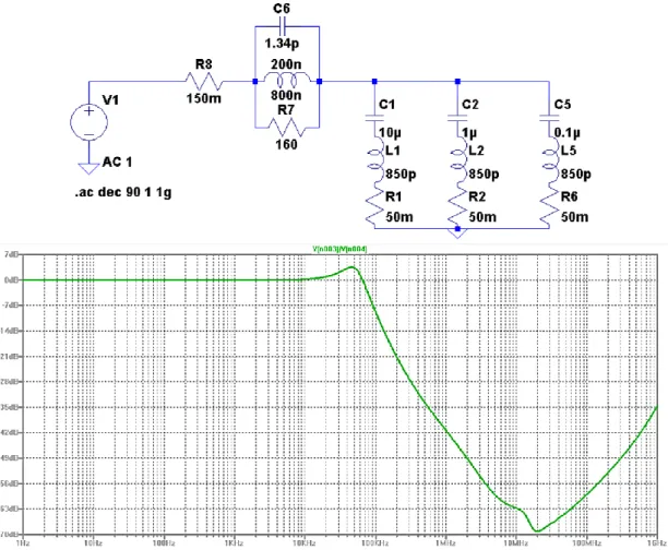
Figure 4-34: RF Component Characterization Results after Fix ... 83
Figure 4-35: PCB Magnetic Field Testing [21] ... 84
Figure 4-36: Results of Radiation Test ... 84
Figure 4-37: Completed Analog Upconverter Device ... 85
Figure 4-38: Analog Upconverter Current Draw ... 86
Figure 5-1: Integrated Jamming Device ... 87
Figure 5-2: Single Tone Output Test for Complete Jammer ... 88
Figure 5-3: Multi Tone Output Power for Complete Jammer ... 89
Figure 5-4: Spectrum Analyzer Capture of Jamming Signal ... 89
Figure 5-5: Spectrum Analyzer Capture with 20 dB Additional Gain ... 90
Figure 6-1: Ideal PSR and PDR Measurements for PHY and MAC Attacks ... 92
Figure 6-2: Physical Test Layout for ZigBee Jamming ... 93
Figure 6-3: Jamming Device Test Setup ... 94
Figure 6-4: Router PANId and Channel During Attack ... 95
Figure 6-5: Router PANId and Channel After Attack ... 95
Figure 6-6: Attack on Coordinator Results ... 96
Figure 6-7: Attack on Router Results ... 97
Figure 6-8: Single Sine Tone Bandwidth over a 2 MHz Span ... 99
Figure 6-9:Single Tone Triangle Wave Bandwidth over a 2 MHz Span ... 100
Figure 6-10: Periodic Jamming Representation ... 101
Figure 6-11: Periodic Jamming Results ... 102
1
1
INTRODUCTION
This thesis report describes the design, building, testing, and analysis of a discrete IEEE
802.15.4/ZigBee jamming device that will jam either a selected number of ZigBee channels or all the ZigBee communication channels. This report will discuss the ZigBee protocol and its
weakness, the general design to exploit the weakness. and the final system design. This report will explain the complete process for creating the jamming device, from initial plan to final construction. It will describe the challenges faced and how these challenges were overcome. The project is structured into two stages (the Digital Synthesizer design and the Analog Upconverter design) and the report will discuss the building and testing of each design. The report will go over the integration of the two designs and the outcome of the ZigBee jamming attempt along with a full characterization of the integrated device.
1.1 Statement of Problem
Sensors are becoming an integral part of the modern world. There are sensors are in our homes, phones, cars, and soon within human beings [1], [2]. These sensors are part of the ever-growing idea of the Internet of Things (IoT). The idea behind the IoT is that all things (humans, machines, data, etc.) are connected to one another. They share data and computing resources to aid in the operation of advanced everyday actions such as autonomous driving, autonomous farming, or keeping track of stock in a grocery store. IoT is being implemented for safer, more efficient, and more reliable operations in day to day life. The term “smart” is not just for phones anymore. Now with the growing idea of IoT there are smart homes, smart hospitals, smart farms, and of course smart cars.
The use of sensors and communication nodes are required to enable real time, intelligent monitoring and control of IoT network. Although, wired solutions have been used in the past, over the past decade wireless communication sensors have been the focus. This is due to the
2
accessibility and the ease of implementation of low cost, low power, complete communication devices often integrated on a single chip [2]. Although developed independently from IoT, the Wireless Sensor Network (WSN) has become an essential concept for IoT design [2]. A WSN is a large network of sensor nodes that sense physical quantities such as light, pressure, and
temperature within an environment. They also have the ability to control the environment and therefore allow for an interaction between the environment and a controller whether it be a person or a computer. [2]
As with any wireless communication method, extra security precautions must be taken. This is because a signal is much more vulnerable to interception (eavesdropping) or interruption
(jamming) when it is propagating through free space rather than when it is propagating through a cable [3]. This additional security risk must not be taken lightly especially when a sensor is linked to the safety or security of the end user. This is a prominent concern as WSNs begin to play large roles in vehicles, medical devices, and home security devices [4]. Additionally, due to the limited unlicensed ISM frequency bandwidth, any new wireless communication protocols must
minimally interfere with current protocols already operating in the same frequency range [5]. This concept is called Wireless Coexistence, and the design decisions used to ensure Wireless
Coexistence are believed to be a cause of a large security risk in the IEEE 802.15.4/ZigBee protocol.
1.2 IEEE 802.15.4/ZigBee Background
In 2003 IEEE released the 802.15.4 standard [6]. This standard was designed to meet the wireless sensor requirements by enabling low cost, low data rate, low complexity, and low power
consumption wireless communication. The IEEE 802.15.4 standard specifies the RF Link Layer and the Data Link Layer. As with most other IEEE 802 standards, this allows for industry to create protocols that integrate with the existing standard by stacking software protocol layers onto the existing link layer defined by 802.15.4. One of the most popular protocols stacked onto the
3
existing layers of the 802.15.4 standard is the ZigBee Mesh protocol created by the ZigBee Alliance. Figure 1-1 shows how the layers defined by the 802.15.4 standard and the layers added by the ZigBee protocol combine to create a wireless network device [7].
Figure 1-1: The ZigBee/IEEE 802.15.4 protocol stack [7]
ZigBee has begun to dominate the WSN field due to the better applicational performance when compared to WIFI or Classic Bluetooth [8]. For example, in a large wireless sensor network like thermometers throughout a farm, there could be hundreds of sensors throughout the network many of which run of a small battery. The power savings, cost savings, and large device support of the ZigBee protocol make it the top choice for wireless sensor networks [8]. Figure 1-2 compares some of the ZigBee performance specifications with that of other top wireless communication protocols.
4
As mentioned above, the ZigBee protocol can be deployed in a mesh network topology. The mesh network topology also allows for the ability to communicate over large distances by hopping the message from one radio to another. To allow this mesh network to work properly, every 802.15.4 standard network has two different types of radio classifications: a full function device (FFD or router) and a reduced function device (RFD or end device). Both routers and end devices can have non-communication roles such a sensors or controllers but typically routers have a constant power source while an end device is typically battery powered and has a low complexity role such as operating a switch. In addition to FFD and RFD radios, one device is assigned as the PAN coordinator which is responsible for managing all the other devices on the mesh network as well as routing the information to the end user or application. An FFD can transmit and receive information from another FFD, PAN, or associated RFD while an RFD can only transmit and receive information with a single FFD (which can include the PAN
coordinator). Figure 1-3 shows an example of the ZigBee mesh network topology [6].
Figure 1-3: ZigBee Mesh Network and Device Types [6]
As with other IEEE 802 standards, the IEEE 802.15.4 standard specifies the RF link layer and the Data Link Layer. The RF Link Layer consists of a RF layer which is the physical medium in
5
which the information is passed and a PHY or physical layer which controls the RF channels and data transmission. The Data Link Layer consists of the Medium Access Control (MAC) layer and the Link Layer Control. The MAC layer provides an interface between the higher layers and the PHY layer.
The PHY describes the frequency band utilization, data rates, modulation schemes and many other requirements needed to transmit and receive information over a wireless channel. In the PHY of IEEE 802.15.4 there are three bands and 27 total different channels. This thesis project focuses on the 2.4 GHz band which contains 16 channels, channels 11-26. The channel spacing is 5 MHz and the channel bandwidth is 2 MHz. Equation 1-1 gives the channel center frequencies with respect to channel number. Figure 1-4 shows the channel distribution at the 2.4 GHz band.
FC= 2405 + 5(Channel − 11) MHz (1-1)
Figure 1-4: Arrangement of Channels in IEEE 802.15.4 2.4 GHz Band [7]
The 2.4 GHz band uses an Offset Quadrature Phase Shift Key (O_QPSK) modulation scheme which allows for a data rate of 250 kbps [9]. For security against random errors and multipath issues, the PHY layer employs a Direct Sequence Spread Spectrum (DSSS) within each channel. Combining QPSK and DSSS means that 4 bits of information are packed into one symbol, and each symbol is then chipped at 32 chips per symbol at the 2.4 GHz band [9]. The PHY layer also is responsible for energy detection. The energy detection command is given by the MAC layer when using Carrier Sense Multiple Access with Collision Avoidance (CSMA-CA) to control the channel utilization. The command is called the clear channel assessment (CCA) [10]. This channel control helps reduce interference between devices and helps wireless coexistence by
6
insuring that the standard does not transmit over any other RF signals within the same band. CSMA-CA works by first checking the channel for any power before the radio can transmit. If the channel is busy, by either another RF signal such as Bluetooth or WIFI or by another IEEE 802.15.4 radio on the same mesh network, the radio waits for a predetermined amount of time before checking the channel again [6]. This is the design decision in the IEEE 802.14.5 standard that this thesis work will exploit.
By placing power within a channel, any device using that channel will be forced to wait for the channel to open. If the channel does not open, the transmission is considered a failure. This CSMA-CA logic flow can be seen in Figure 1-5.
7
Figure 1-5: The Basis slotted CSMA mechanism in IEEE 802.15.4 [7]
If power is placed in all the 16 channels of the 2.4 GHz band, the IEEE 802.15.4 standard, and subsequently any protocols using the standard such as ZigBee, will fail to transmit.
8
2
DESIGN OVERVIEW
This project has two objectives. The first and main objective is to produce a device that will create a 16-tone signal to exploit the weakness in the 802.15.4 standard and completely disable a mesh network from any data transmission to or from the PAN coordinator radio. This device will produce a tone in each of the 16 channels (channels 11-26) in the 2.4 GHz band of the IEEE 802.15.4 standard. The secondary objective is to create a device that will be used as a teaching tool by interfering with select IEEE 802.15.4 channels and monitoring the ZigBee mesh network and its response to the interference. To aid in this disturbance, the device must be able to place power in selected channels and leave other channels open to properly monitor the ZigBee dynamics.
Combining the two objective leads to a device that can create a multitone signal with any combination of tones ranging from 2405 MHz to 2480 MHz in 5 MHz increments. Figure 2-1 shows how the spectrum of this device will look both in the full jamming mode and the channel interference mode.
Figure 2-1:16-tone Signal used for complete ZigBee Jamming (top). Multi-tone Signal used for channel interference in Channels 1-3 while the remaining channels are left open (bottom).
9
2.1 Multi-tone Signal GenerationThere are many ways to create a multi-tone signal with 5 MHz spacings but by adding the
requirement of selecting any combination of frequencies, the problem becomes more challenging. The first consideration was to use a step recovery diode (also known as a frequency multiplier) to create the 5 MHz harmonics followed by selective filters to choose the desired signals [11]. In theory, the step recovery diode is not difficult to implement and was simulated using Advanced System Design (ADS). Figure 2-2 shows the result of the simulation.
Figure 2-2: ADS Step Recover Diode Simulation
Although the step recovery diode is not difficult to implement, there are many problems that make it a poor approach for this project. The main issue is having a series of filters to condition the signal and to select the different channels. The 5 MHz component is roughly 20 dB larger than the next harmonic. Additionally, the power level after the last required 80 MHz tone does not drop off. Filters would be needed to isolate the 5 MHz to 80 MHz range and to help flatten the response of the tones. A filter of this specific purpose would be hard to find or build.
10
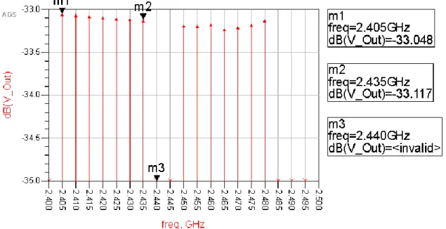
Additionally, a series of band stop filters would be needed at each harmonic along with a bypass to enable and disable any combination of desired tones. Lastly, a mixing circuit would be required to mix the entire signal up to 2.4 GHz. The series filters would cause the jammer to become very large physically and require repetitive work not beneficial to thesis research. The next option was to use frequency synthesizers or phase locked loops with integrated voltage-controlled oscillators. This method would require 16 frequency synthesizers and 15 couplers such as a branch line coupler. The biggest benefit of this design is the accuracy of the tones and the simplicity of the design. By using frequency synthesizers every desired tone could be created from 2.405 GHz to 2.480 GHz which removes the need of filters and mixers. Additionally, this method makes turning off any tone very easy by simply disabling the synthesizer. Since most synthesizers have 50 Ohm outputs, disabling it simply acts like a 50 Ohm termination on one of the coupler inputs. This method was also simulated using ADS. Figure 2-3 shows this simulation with the two center frequencies (2.440 and 2.445 GHz) disabled.
Figure 2-3: ADS Simulation of16 Frequency Synthesizers and 15 Couplers with channels 18 and 19 Disabled
11
The problems with this approach are cost, layout size, and layout complexity. The MAX2870 dual output PLL with integrated VCO was the best choice for this approach. Since this device is a dual output device, a total of 8 of these PLLs would be needed. At a cost of over $11 each, this would cost more than $90 in just the PLL not including board design and other components needed. This PLL, along with most others, is digitally controlled and requires a micro-controller to operate adding to the cost and complexity. The footprint of the MAX2870 is 32 Thin Quad Flat Pack No-Lead (TQFN) meaning there are 32 connecting pads that can only be soldered using a heat gun or reflow oven [12]. Figure 2-4 shows this footprint.
Figure 2-4:MAX2870 32 TQFN Footprint [12]
Trying to create a PCB design with 8 of these synthesizers along with the necessary passive devices, microprocessor, and power supplies would be very complex. This design would also require 15 couplers which would add to the complexity and size of the PCB design. This design was ruled out do the high cost estimate, PCB design complexity, and PCB size estimate. The next consideration focused on high speed digital to analog converters (DAC). The original plan was to use a microprocessor to load a standalone first in first out (FIFO) with a discrete
12
version of the multi tone signal. Then the FIFO would feed the highspeed DAC using a single PLL. This design was preferred due to the broad scope of the project along with the ability to change the output signal to any desired signal by simply changing some code in the
microprocessor. Further research showed that instead of a separate PLL, microprocessor, and FIFO, all these devices could be combined onto one FPGA (field programmable gate array).
2.2 Top Level Overview
The final design proposition included an FPGA that feed a highspeed DAC. This FPGA sends the DAC the discrete version of the multitone signal from 5 MHz up to 80 MHz. From there the signal would be mixed up to 2.4 GHz and then amplified before being radiated by an antenna. Figure 2-5 shows the early block diagram for the final design proposal.
FPGA
Highspeed
DAC
IF RF LO MIXER DATA 10 CLKAMP
OSC
AntennaFigure 2-5: Early Top-Level Block Diagram
The FPGA allows for a much simpler block diagram by combining the microprocessor, the PLL, and the FIFO all into one unit. Also, the FPGA is beneficial because it is customizable. If there is a problem with the FPGA design, it can easily be fixed using software. This design also allows for many different applications if desired by future users. By changing the HLD code one could
13
change this jammer into a broadcast device or a spoofer. Expanding on the idea of future uses, it was decided that this design would be split into two separate boards.
Separating this design into a digital frequency synthesizer board and a 2.4 GHz up
converter/amplifier board one could use these devices separately for many other applications. The digital frequency synthesizer could create any desired signal from 1 MHz to 105 MHz including a modulated signal using digital modulation within the FPGA. The analog upconverter would be useful in mixing any input signal up to 2.4 GHz. Separating the analog and digital into two separate boards helps reduce the complexity in mixed signal and highspeed PCB design. The Digital board would deal with issues in mixed signal design, but it would be relatively low frequency. The analog board would have no digital design concerns but at 2.4 GHz, high
frequency design would need to be taken into consideration. The separated boards can be seen in the block diagram in Figure 2-6.
Digital Synthesizer Board
FPGA
Highspeed DACAnalog RF Board IF RF LO LT5560 MIXER DATA 10 CLK AMP
OSC
AntennaFigure 2-6: Block Diagram with Separate Boards
2.3 Device Requirements
As a jammer, this device is required to produce 16 tones from 2405 MHz to 2480 MHz with enough power for the 802.15.4 PHY layer to consider that the channel is in use. In IEEE 802.15.4
14
the clear channel assessment (CCA) uses the energy detection (ED) mechanism to decide whether a channel is open or not. If there is any energy above the ED threshold, the channel is considered taken. The ED threshold is 10 dB above the maximum allowed receiver sensitivity [10]. In the ZigBee protocol the maximum receiver sensitivity for channels 11-26 is -85 dBm [7]. This means that if a channel has a power of at least -75 dBm at the receiver, the channel is considered
occupied.
The for this project, the jamming device is required to attack a network within the same room. With a jamming distance of roughly 3m, the jamming device could be placed anywhere within a small room and still attack a network. Equation 2-1 is the Friis power equation and it is used to calculate the power budget of a wireless link.
𝑃𝑟 =
𝑃𝑡𝐺𝑡𝐺𝑟𝜆2
(4𝜋𝑅)2 (2-1)
By knowing the gain of both the receiver and transmitter antennas, wavelength, distance between radios, and the transmit power, one can calculate the received power. This equation can be rearranged to solve for the transmit power required for the receiver to detect a minimum of -75 dBm with the jammer at 3 meters away. The gain of the antenna on the jamming device is 5 dBi and the maximum gain of the Digi XBee PCB antenna is 1.5 dBi [13].
𝑃𝑡 = 𝑃𝑟(4πR)2 𝐺𝑡𝐺𝑟𝜆2 = 10 −7.5(4𝜋 × 3)2 100.5× 100.15(2.998 × 10⁸ 2.4 × 10⁹ ) 2= 644.7 nW = −31.9 dBm (2-2)
Equation 2-2 shows that at least -31.9 dBm transmit power is needed per channel to jam the ZigBee radios at 3 meters from the coordinator. Doubling (adding 3 dB) the power four times results in the combined output power for all 16 tones to be -19.9 dBm.
It is required that the output power of the jamming device be adjustable. The analysis above calculated the minimum power needed. Ideally, the output power of the jamming device should be well over the minimum while also being able to achieve the minimum power and slightly below minimum power. This would allow better analysis of jamming the 802.15.4 standard
15
including testing at what minimum transmit power the device successfully jams the ZigBee radios. To meet this requirement the Analog Upconverter will rely on a variable gain amplifier (VGA) or a variable attenuator.
This device must easily be able to change what tones are activated without having to reprogram the FPGA. This will allow quick changes to the jamming signal to see how the ZigBee protocol reacts when a transmitting channel becomes occupied. This will require 16 dip switches
16
3
DIGITAL SYNTHESIZER DESIGN
3.1 Overview
The digital synthesizer was designed to work by using the on board read only memory (ROM) on the FPGA to store one period of discrete data from each channel center frequency. The on-board switches would then select which ROMs would be routed to a summing and normalization block. The summing and normalization block would sum all the data in the selected ROMS and then divide the results by the total number of signals selected. The output of the
summing/normalization block would then feed the FIFO. Once, the entire period is loaded, the output of the FIFO will feed both the DAC and loop back into itself for continued signal output. Figure 3-1 shows the early block diagram for the FPGA design.
ROM0 (5 MHz) ROM1 (10 MHz) ROM15 (80 MHz) Mu x_0 x0000 SW0 M u x_1 x0000 SW1 Mu x_1 5 x0000 SW15 10 10 10 SUM_NORM IN_0 IN_1 OUTPUT IN_15 10 10 10 FIFO DATA_IN DATA_OUT 10 FI FO _MU X 10 10 OUTPUT to DAC
Figure 3-1:Early FPGA Block Diagram
The key of this design is that every ROM block contains one period of digital data and that the period of data is then repeated within the FIFO. After the FIFO, the digital signal is ported out of the FPGA using the IO (in-out) ports and feed into the DAC along with the DAC clock signal.
17
The DAC will convert the signal into an analog waveform where it can be routed to the analog board for mixing and amplification.
3.2 FPGA Design
Before any FPGA design could begin, a FPGA brand, product family, synthesis software, and simulation software would need to be chosen. The Xilinx Artix 7 with Vivado was an easy choice due to the familiarity with these resources from previous course works. The Bases 3 development boards with Artix 7 FPGAs were readily available for use and the Vivado software pack
contained everything needed for synthesis, implementation, and simulation. Using Vivado, a very rudimentary draft of the system was designed to get a rough idea of the hardware and resource utilization required by the design. Figure 3-2 shows the results of the implementation.
Figure 3-2: First Run FPGA Implementation Results
By referencing the Xilinx Artix 7 family table, one can see that the resource utilization of the hardware is roughly 5% of the smallest FPGA offered by the family [14].
The signal degradation issues when interfacing with highspeed DACs meant that an FPGA development board could not be used. Since a custom board was to be designed, component packages were considered to simplify the manufacturing process and to greatly reduce cost. One of the considerations was to avoid a component with a ball grid array. Ball grid arrays require multiple layers along with blind and buried vias to route all the signals away from the FPGA to other components. All the Artix 7 FPGA come in some sort of ball grid array. This along with the high cost of the Artix 7 caused it to be a bad choice for this project.
The Xilinx Spartan 3A is a modern redesigned version of the older Spartan 3. The Spartan 3A comes in many packages including Quad Flat Pack and Ball Grid Array. The Quad Flat Pack is
18
only offered in the 50k and 200k gate sizes. The Spartan 3A in quad flat pack is much easier and cheaper to implement and is 4 times cheaper to purchase than the Artix 7.
In addition, I.O pads, PLL Clock speeds, and I.O standards must be considered before committing to an FPGA. At this point, the DAC had not yet been chosen but specifications for interfacing were known. From the Nyquist Criterium, the sampling rate and clock signal into the DAC from the FPGA must be no less than 160 MSPS or MHz (twice the highest frequency of 80 MHz). The DACs in consideration ranged from a sampling rate of 200MSPS to 500 MSPS and ranged from 10 to 16-bit parallel feed. This would require at least 16 200-500 MHz data outputs all on the same side of the FPGA Quad Flat Pack. Lastly the communication standard required from the DACS in consideration were Low Voltage CMOS (LVCMOS) and Low Voltage Differential Signals (LVDS).
By referencing the Spartan-3A FPGA Family Data Sheet [15], one can see that the Spartan-3A meets all of the above requirements. The I.O capabilities section of the data sheet detail the supported interfacing standards which include LVDS and LVCMOS. Under the Features section, the data sheet states that the Digital Clock Mangers can create frequencies ranging from 5 MHz to 320 MHz. This eliminates the DACs in the 500 MSPS range but still allows proper interfacing with the lower 200-300 MSPS DACs. Lastly, within the Pinout Description section of the data sheet, it states that the smallest package (VQ100) contains a total of 68 different I.O ports for single ended interfacing and or 60 different I.O ports for differential interfacing. The package foot print from the data sheet, Figure 3-3, show than any side of the FPGA has enough IO ports to feed the DAC.
19
Figure 3-3:VQ100 Package Footprint - XC3S200A (Top View) [15]
At this point the Spartan 3A using the VQ100 package seemed to be a good fit for the project. Unfortunately, the Xilinx Vivado FPGA design software does not support the Spartan 3A and so the old ISE Design Suite had to be used. Figure 3-4 shows the black box diagram for the HDL code written on ISE Design Suite.
20
ROM0 (5 MHz) ADDR DATA SCLK ROM1 (10 MHz) ADDR DATA SCLK ROM15 (80 MHz) ADDR DATA SCLK M u x_ 0 x0000 SW0 M u x_ 1 x0000 SW1 M u x_ 1 5 x0000 SW15 10 10 10 SUM_NORM IN_0 IN_1 OUTPUT IN_15 10 10 10 PRE_FIFO DATA_IN DATA_OUT PRE_WE PRE_FULL PRE_RE SCLK DAC_CLK 10 FIFO DATA_IN DATA_OUT FIFO_WE FIFO_FULL FIFO_RE DAC_CLK 10 FI F O _ M U X 10 10 s_dac_clk s_pre_we s_pre_re s_sclk s_fifo_we s_fifo_re s_dac_clk s_pre_full s_fifo_full s_ fi fo _m u x CONTROLLER FSM PRE_FULL PRE_WE FIFO_FULL PRE_RE RST FIFO_WE FIFO_RE FIFO_MUX ADDR SCLK DAC_CLK s_fifo_full s_pre_full s_sclk s_dac_clk s_pre_we s_pre_re s_fifo_we s_fifo_re s_fifo_mux s_addr s_addr s_addr s_addr s_sclk s_sclk s_sclk DCM SCLK DAC_CLK s_dac_clk s_sclk s_buttonFigure 3-4: Spartan 3A FPGA Black Box Diagram
The FPGA hardware starts with 16 ROMs that contain the digital data for each of the 16 channel tones. The ROMs were created by using the Xilinx IP (intellectual property). The ROMs could be loaded manually in the code or by using a coe file. The coe file was a better choice for ease of modifications in the future. Additionally, at this point, the DAC was not chosen, so the sampling rate and word size were unknown. By using coe files, the data in the ROMs could easily be changed. MATLAB was used to create the coe files. The MATLAB script requires sampling rate, desired frequencies, and word length as inputs and then output a coe file for each desired
frequency. Within the coe files are binary numbers that create a digital waveform at the desired channel frequencies. To ensure each coe file had the same number of words, the higher
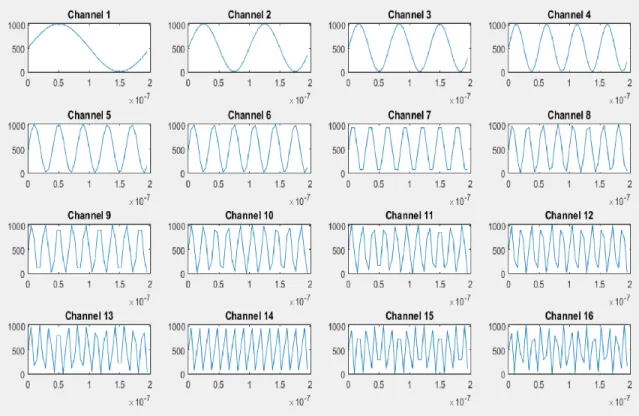
frequencies had multiple periods in them. The MATLAB script can be seen in the Error! R eference source not found.. The output of the MATLAB code can be seen in the visual representation in Figure 3-5. Note that at the higher frequencies the low sampling rate degrades the time domain signal but according the Nyquist Criterion, no information is lost.
21
Figure 3-5: MATLAB Waveform Creator Output for ZigBee at 210 MSPS and 10-bit Words
Multiplexers are placed after the ROMs and either pass the ROM data or pass a 10 bit zero. The Multiplexers are controlled by the physical switches that will be placed on the board. The signals from the multiplexers are routed to custom block called SUM and NORM. This block sums all the inputs and then divides the results by the number of switches that are on. This insures that the output of the FPGA will always use the full-scale range of the selected DAC.
Following the SUM and NORM block, two separate FIFOS are needed due to the two different clock speeds. All hardware up to the first FIFO runs at the CLK speed and the hardware
following the first FIFO runs at the DAC CLK speed. The CLK is a slower clock signal that will come from an external oscillator. The DAC CLK is a fast clock created by using the slow CLK and a PLL. The DAC CLK runs the second FIFO and will be output to the DAC as well. The original plan was to use just one FIFO and multiplex the CLK and DAC_CLK into the FIFO CLK input. This was not advised due to the speed specific pathlengths used when implementing the FIFOs. Instead, two FIFOs were used. The PRE_FIFO is a two clock FIFO where the write
22
clock is the slower FPGA clock and the read clock is the faster DAC clock. The second FIFO reads and writes at the DAC clock.
IDLE
FIFO_rst=0
FIFO_RE=0
FIFO_LOOP=0
STATE=00
LOAD2
PRE_WE=0
PRE_RE=1
FIFO_WE=1
STATE=10
LOAD1
PRE_WE=1
count_on=1
STATE=01LOOP
PRE_RE=0
FIFO_RE=1
FIFO_LOOP=1
STATE=11
RST=0
RST=1
count_rst=0
PRE_FULL=1
count_on=0
FIFO_FULL=0
PRE_FULL=0
RST=0
FIFO_FULL=1
RST=1
FIFO_rst=1
INPUT
OUTPUT
23
A physical button was placed on the board to start the run sequence. When the button is pressed, the data from the ROMs flows through the multiplexers and SUM and NORM block and loads the PRE_FIFO at the slower FPGA clock. When the PRE_FIFO is full with a complete period of data, the data is read from the PRE_FIFO and writes it into the FIFO at the faster DAC clock. Once the FIFO is full, the data is read from the FIFO and is sent to both the DAC and loops back to write into the input of the FIFO. This whole process is controlled by the controller block which consists of two finite state machines (FSM) one running at each of the two clock speeds. Figure 3-6 shows the FSM diagram for the controllers as one single state machine. The second state machine was added during the simulation and testing process due to strict timing constraints. Note that to simplify the diagram only outputs that values’ have changed are displayed in the state.
After completing the design, it was synthesized to see what resources the design would use. Before synthesis, the smallest Spartan 3A was chosen, XC3S50A. After synthesis the design utilization summary showed that the number of occupied slices was 880 while the XC3S50A only has 704 slices. The design was then changed to be implemented on the XCS200A which has 1792 total available slices [15]. Figure 3-7 shows the Xilinx ISE Design Suite Device Utilization Summary.
24
Figure 3-7: ISE Design Suite Synthesis Results with XC3S200A
To test the proper functionality of the code, Xilinx iSim FPGA simulator was used. The
simulation set the desired switches to the on position and then activated the run button. Due to the precise timing of the design, much time was spent adjusting signal delays. By using D flip flops and alternating the use of Mealy and Moore FMS design, the timing of the control signals was adjusted until proper operation occurred. This also allowed for a period of the output data to be collected and analyzed. Figure 3-8 shows a screenshot of the iSim simulation with the FPGA data output signal in purple.
Figure 3-8: Xilinx iSim FPGA Simulation showing the Data Output in Purple
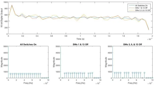
The iSim output data was collected and plotted using MATLAB. Three simulations were
25
cases showed that the FPGA code worked as designed. The three simulation results can be seen in Figure 3-9.
Figure 3-9: FPGA iSim Data plotted using MATLAB showing the Time Domain (top) and the Freq Domain (bottom)
It is important to understand that the DAC has an impact on the quality of the output signal. This will cause the frequency spectrum to have undesired qualities. The operation of the DAC can be estimated using a sample and hold operation. Instead of ramping to each digital data point, the DAC (almost) immediately steps to the data point and holds at the level until the next data point. This impulse contains theoretically infinite frequencies just as a square wave does. This causes the output of the DAC to have a sinc roll off like a square wave. Figure 3-10 demonstrates the sample and hold time domain operation and the sinc roll off frequency domain results.
26
3.3 Choosing PartsBefore any design could be done, components of the system needed to be chosen. The two main components for this design is the FPGA and the DAC. In addition, an oscillator, an FPGA programmer, switches, connectors, and power supplies are needed. In the last section the Spartan-3A XC3S200A in the TQFP100 package was chosen for the FPGA. Each component has specific requirements but there are a few general requirements for all components. The data sheet
indicates that the FPGA requires an internal power supply voltage of 1.2 VDC and an auxiliary power supply voltage of either 2.5 VDC or 3.3 VDC. To simplify the design and reduce the number of power supplies needed, all other components should require the same voltages. As with the FPGA, no ball grid array style packages will be used, and it would be preferred that all components have leads.
The most important specification of the DAC is the sampling rate. This is the speed at which new words (or digital values) are feed into the DAC. Theoretically, the sampling rate must be larger than twice the highest desired frequency. Since the highest frequency for this project is 80 MHz, the sampling rate must be larger than 160 mega samples per second (MSPS). From the previous section, the maximum FPGA PLL output clock is 320 MHz, so the maximum DAC input clock speed is 320 MSPS. The highest speed DAC that is under 320 MSPS is the Analog Devices (AD) 210 MSPS D/A Converter. The next step up is the TI DAC31x1 D/A converter which is capable of 500 MSPS. The TI is advantageous because the clocking speed would be half of the maximum ability of the DAC resulting in better performance when compared to maxing out the abilities of the Analog Devices D/A Converter. Both DACs are available in 10 or 12-bit resolution although 10 bits was selected to aid in the simplicity. The AD DAC communicates with FPGAs using 3.3 V low voltage CMOS (LVCMOS33) while the TI DAC uses low voltage differential signal (LVDS) both of which are compatible with the Spartan-3A FPGA. LDVS is used because of the good signal integrity caused by parallel lines with apposing currents to cancel out magnetic fields
27
but it requires two traces for each bit, doubling the complexity when designing the PCB. The simpler to implement LVCMOS33 made the AD DAC the better choice along with lower cost, leaded package, and ease of implementation [16], [17].
The next component chosen was the oscillator used as the clock input for the FPGA. The oscillator was chosen to reach the entire frequency range of the FPGA with the PLL. The on-board FPGA PLL can multiple and divide by 32 and the FPGA operating frequency range is 5 to 320 MHz. Equations 3-1 and 3-2 show the minimum and maximum oscillator frequencies.
𝐹𝑜𝑠𝑐 𝑚𝑖𝑛=
320 𝑀𝐻𝑧
32 = 10 𝑀𝐻𝑧 (3-1)
𝐹𝑜𝑠𝑐 𝑚𝑎𝑥= 32 × 5 𝑀𝐻𝑧 = 160 𝑀𝐻𝑧 (3-2)
By using the frequency range define above, along with the 3.3 V requirement and the LVCMOS standard requirement the SiTime 5001 series Oscillator at 40 MHz was the best fit. Although this device is a QFN (quad flat no lead) package, it has only 4 pads that are over 2 squared millimeters each which should be relatively easy to solder using solder paste and a heat gun [18].
The next important component of the Digital board design was the FPGA configuration method, or in other words, the FPGA programmer. When the synthesis and implementation are complete in the Xilinx ISE Design Suite, the program generates at bit stream. This bit stream is what is used to configure the FPGA. There are many different methods for configuring the FPGA which include many different types of non-volatile memory to enable an auto-configuration when the board is powered on. The non-volatile memory can be loaded into the FPGA via the self-loading master configuration or it can be loaded in the slave mode using a separate microprocessor. Un fortunately some sort of processor is required to load the data onto the non-volatile memory in the first place. The simplest method is to use the JTAG configuration mode which uses an IEEE standard for the configuration and uses a standard style 2x6 pin header that has four
interconnections with the FPGA. Figure 3-11 shows the JTAG Configuration Interface. Note that this interface can be used to program a chain of FPGAs but for this project only one FPGA will
28
be programmed. In addition to ease of implementation, the JTAG protocol can also be used to aid in debugging the FPGA which is very useful when dealing with highspeed signals that cannot be probed [19].
Figure 3-11: JTAG Configuration Interface [19]
Digilent makes a USB to JTAG dongle that connects the Xilinx 2x6 JTAG header to a USB. Additionally, Digilent makes a surface mount JTAG to micro USB board that solders directly onto a PCB board. Both options were considered but for roughly the same price, the JTAG-SMT2 was the better choice in case the JTAG cable was lost or became damaged. Since the JTAG-SMT2 is soldered directly to the board, it cannot be lost, and the generic micro USB cable used is cheap and easy to replace. The JTAG-SMT2 uses the same 4 interconnections with the FPGA as the JTAG dongle.
The last components required are the power supplies. Every component on the board uses 3.3 VDC besides the FPGA internal power which is 1.2 VDC. The DAC requires two separate 3.3 VDC supplies, one for the analog portion of the integrated circuit and one for the digital portion of the integrated circuit. A total of three power supplies will be needed, a digital 1.2 VDC supply for the internal FPGA, a digital 3.3 VDC supply for the FPGA AUX power, the JTAG power, the
29
digital side of the DAC, and the oscillator power, and lastly an analog 3.3 VDC supply for the analog side of the DAC.
To properly size the power supplies, current draw estimations are required for each supply. This can be done for most of the components by looking at the data sheets for expected current draws. For the FPGA, the clock speeds and aux voltage are set within the constraints file. The constraint file is used to apply constraints on the FPGA implementation such as voltage, clock speed, and IO pin selection. With the proper constrains, the ISE Design Suite can be used to make dynamic and quiescent power estimations. Figure 3-12 shows the total estimated current draw for each of the three power supplies.
Figure 3-12: Digital Design Power Estimations
Since this digital board is very sensitive to noise and has no power efficiency requirements, the best power supply option is a low drop out (LDO) voltage regulator instead of a noisy DC-DC converter. The LDO is a good option because there is no internal switching to change the voltage, instead the voltage is reduced by simply dissipating the extra power in heat. This makes the LDO inefficient but a low noise power supply. The best fit for the previous requirements was the Diode Incorporated AP212x series highspeed, extremely low noise, LDO regulators. Although this project will mostly be used on a bench, in the rare occurrence that it needs to be battery powered, the LDO max input power would need to be greater that 6V or 4 series 1.5 V batteries. 6 V was used instead of 4.5 V because of the knowledge that the analog board would be using 5 V output
Component ADVCC33 (mA) DVCC33 (mA) DVCC12 (mA)
DAC 36 9 N/A
OSC N/A 33 N/A
FPGA EST Q N/A 16 8
FPGA ESTDyn N/A 18 27
LEDs N/A 10 N/A
30
LDOs. To insure plenty of current leeway two 300mA VDC AP2125 LDOs were used for the 3.3 VDC supplies and one 150 mA AP2120 LDO was used for the 1.2 VDC supply.
3.4 Schematic Design
Before any design could begin, a schematic symbol and corresponding layout footprint is needed for each component used on the digital board. Since all components were sourced from Digikey, some of them had downloadable part libraries which contained both the layout and symbol for the design. This was the case for both power supplies. For those that did not come with a library, a web service named Symacsys Component Search Engine was used to either find a library for the desired component or it would create the library for free usually in less than 24 hours. For some of the simpler components such as headers, switches, and push buttons, the libraries were created manually using the tools on Autodesk Eagle PCB design software.
Using the symbols in the libraries created and Eagle, the schematic for the entire digital board was created. This was done by first placing the FPGA and the DAC and routing the
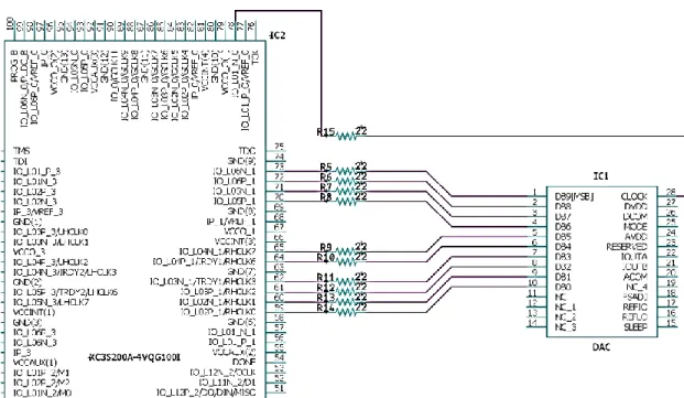
interconnections. There are total of 11 interconnections between the FPGA and the DAC, one connection for each of the 10 bits and then one connection for the clock. Figure 3-13 shows the interconnection between the FPGA and the DAC along with a 22 ohm series resistor. The resistor is used to aid in the 50 ohm termination. Although the Spartan-3A states that no termination is required for LVCMOS, the AD9740 DAC shows the series 20 ohm resistors on the schematic of the development board. The resistors could easily be replaced with no-load resistors if the 20 ohm termination causes any problems [19], [17].
31
Figure 3-13: FPGA-DAC Interconnection
Next the switches and push buttons were added to the circuit. Generic surface mount push buttons and switches were selected. S1 and S2 are two 8 bank single pole single throw switches that are connected to 16 IO ports on Bank 2 of the FPGA. These 16 switches will control the 16 channels. The FPGA has internal programmable pull up/down resistors but to insure no issue would come up, an external pull up resistor network was added to the switches. S3 is also connected to Bank 2 on the FPGA and it will be used to start the FSM. S4 was connected to the PROG_B terminal on the FPGA and it is used to reset the FPGA if needed. Figure 3-14 shows the schematic of the switches added to the FPGA
32
Figure 3-14: Digital Synthesizer Switch Banks
The output of the oscillator was simply connected a global buffered clock input on Bank 0 of the FPGA. No termination was used in the interconnection. This matches the schematic of the Spartan-3A development board. The JTAG-SMT2 was connected using the schematic found on the JTAG SMT2 datasheet which can be seen on Figure 3-15. Typically current limiting resistors are required on all signals but since both the JTAG voltage and the FPGA auxiliary voltage are 3.3 V, this is not needed [19], [20]. Figure 3-16shows a schematic capture of the JTAG and Oscillator interconnections with the FPGA.
33
Figure 3-15:JTAG-SMT2 to FPGA connections with Current Limiting Resistor[20]
Figure 3-16: Interconnections between the JTAG-SMT2, Reset Switch, Oscillator, and FPGA
Two sets of headers were added to the design. One was used as a set of test points connected directly to 6 IO ports on the Bank 3 of the FPGA. In the future, any desired signal could be routed out of the FPGA onto a pin on the header. The other header was used to control the configuration mode. The JTAG-SMT2 can configure using either JTAG or SPI so this header was added in case there were any issues with the JTAG protocol. The Mode header was connected using pull up
34
resistors on one terminal and pull down on the other. A jumper across the terminals would bring the mode selector from 1 to 0. There are three total mode selectors.
The power and grounding portion of the schematic required much more though and analysis. Separate grounds are required for the digital and analog portions of the board, decoupling capacitors are required throughout the board, and filtering is required to reduce the amount of digital noise entering the analog circuit. When considering mixed signal (digital and analog) designs, it is very important to separate the components, their power, and their grounds. This is because digital circuits especially those made from MOSFETs have large surges in current when the gate switches. Combine millions of gates together and the switching current can cause noticeable deviation on the power and ground rails. The best way to help combat this is to use a bypass capacitor. A bypass capacitor is a capacitor placed between the power and ground rails of an integrated circuit. The bypass capacitor helps by supply the circuit with extra current when the power rails cannot keep up with the demand. Another way to think of the bypass capacitor is an AC short to ground which helps eliminate the digital noise cause by switching.
Properly sizing bypass capacitors, it crucial to the performance of the circuit. The following are a few rules of thumb when choosing bypass capacitors.
• The higher the frequency, the smaller the capacitor.
• Use parallel capacitors of different sizes with the closest to the device being small and the capacitor closest to the power supply being large.
• Place the coupling capacitors as close to the device as possible.
• Use development board or datasheet recommendations on capacitor sizes.
By referencing the datasheets of all the devices on the board, 0.1 uF capacitors were selected to be placed next to the devices power inputs and 1 uF capacitors were picked for the outputs of the power supplies. A third set of bypass capacitors were added to be placed somewhere in between
35
the power supplies and the devices in the case where extra bypassing was needed. Lastly the same one 1 uF bypass capacitor was added to the inputs of all three power supplies.
It is important to ensure that this combination of capacitors will have the desired results against the switching noise. The Knee Frequency, Fknee, is used with digital circuits as an estimation of significant frequency. In a digital circuit most of the switching power is concentrated below Fknee while most frequencies above it have little effect on the digital circuit performance. The circuit response at Fknee describes the circuit’s ability to process a step. Equation 3.3 shows the calculation of Fknee and the results from using the oscillator rise time of 1.5 ns. [21]
𝐹𝑘𝑛𝑒𝑒 =
0.5 𝑇𝑅 =
0.5
1.5 𝑛𝑠= 333 𝑀𝐻𝑧 (3-3)
After finding Fknee and the bypass capacitor values, the power delivery circuit can be simulated. For each capacitor an 850 pH inductor and a 50 mohm resistor were added in series to model the parasitics in a 0603 surface mount capacitor. The results of the simulation show that at 333 MHz the impedance to ground is roughly – 9 dB meaning it is a dead short. This simulation indicates that the higher frequencies will indeed short to ground while DC has a high impedance path to ground. The results can be seen in Figure 3-17.
36
Figure 3-17:Bypass Capacitor Simulation Schematic (top) and Results (bottom)
The AD9740 DAC datasheet recommends using a LC filter with a ferrite bead to aid in the removal of digital noise from the analog circuit. A ferrite bead is used instead of an inductor to help eliminate any resonance by having a lossy core which dissipates energy instead of simply storing it. Figure 3-18 shows an example of the LC filter.
37
The Taiyo Yuden HS121 ferrite bead was picked for the inductor of the filter. The capacitor was a similar bypass network as in Figure 3-17 but with an added 10 uF capacitor at the beginning of the chain. To ensure this filter did not have any resonance at Fknee, it was simulated using
LTspice. First a model of the ferrite bead was created using information from the datasheet as well as from the impedance response plot of the ferrite bead. Both the impedance response from the datasheet and from the LTSpice simulations can be seen on Figure 3-19. Figure 3-20 shows the entire LC circuit simulation schematic and results. This results show roughly-45 dB at 333 MHz meaning there should no resonance at the FPGA switching speeds [22].
Figure 3-19 Ferrite Bead Expected Impedance Response (left) and the Impedance Response from the Simulated Model (right)[22]
38
Figure 3-20: LC Filter with Ferrite Bead Simulation Schematic (top) and Results (bottom)
The AD9740 has differential current source outputs. The output could be converted to single end by using just one output or by using a transformer. This was decided against due to most of the RF components in the Upconverter also being differential input and output. The differential outputs had to be converted to voltage outputs. Since two 50 ohm SMA connectors were being used as the output, the current outputs were both shunted with a 50 ohm resistor to ground. With the 50 ohm shunt, the max output voltage must be checked to insure it does not surpass the absolute max output rating listed on the datasheet.
𝑉𝑚𝑎𝑥= 𝑅 ∗ 𝐼𝑚𝑎𝑥 = 50𝛺 × 20𝑚𝐴 = 1𝑉 (3-4)
The absolute max rating for Vout on the DAC is 3.6V which is well over 1 V, so the 50 ohm resistors would cause no issues.
39
A few final details were added to finish the schematic which include:
• Power switch
• Power LED
• Done LED to show programing is complete
• Output On LED
• Mini banana connectors for the 5-6VDC power in
• Test points and current sense resistors to measure current draw
The final schematic for the Digital Synthesizer Board can be seen in APPENDIX B.
3.5 Layout Design
There are numerous concerns regarding the layout of a highspeed mixed signal design. Parasitic affects caused by quick rise times can cause many issues such as cross talk from mutual
inductance in traces. It can also cause inductance within vias which degrade the ability for bypass capacitors to shunt to ground. Improper ground paths can cause ground loops which can further increase cross talk or even cause radiation of signals. Path lengths can cause signal delays which can break the tight timing requirements of a digital circuit. To avoid these issues a good layout plan is required before any layout work begins.
Before any layout design was done using Eagle, a rough plan of the layer stack and component placement was devised. A four-layer stack was chosen since there were no BGA components or size restrictions that would require extra signal layers. The standard four-layer stack used consists of a signal layer, a ground layer, a power layer, and another signal layer.
40
Figure 3-21: Four-Layer PCB Stack
A rough plan was then created of the component placement as well as the power and ground plane designs. Since this is a mixed signal design, two ground planes are required, one for the digital ground and one for the analog ground. This helps keep any digital ground bounce isolated from the analog circuit. The two planes connect near the power supply portion of the board. There are also three different power planes required, one for each of the three power supplies. Figure 3-22 shows the rough layout plan for the design.
41
Figure 3-22: Digital Synthesizer Layout Plan
To start the layout all the components were placed on the 4x5 inch board following the layout plane. The power supplies were moved to the upper right-hand corner of the board due to space limitation. From there the major signals were routed along with any terminations or pull up/down resistor networks. These signals included the FPGA to DAC data signals and 20 ohm
terminations, the JTAG communication wiring, the switch to FPGA signals along with the pull up
POWER SPLY
FPGA
SWITCHESJTAG
D
A
C
SMA SMA POWER SPLYFPGA
SWITCHESJTAG
D
A
C
SMA SMA POWER SPLYFPGA
SWITCHESJTAG
D
A
C
SMA SMADGND
AGND
DVDC33
AVDC33
DVDC12
SIGNAL LAYER GROUND LAYER POWER LAYER42
network, the headers for mode selection and troubleshooting, and the DAC to SMA signal with the 50 ohm shunt terminations.
Trace width was important for the highspeed signals to ensure a 50 ohm characteristic impedance. The traces on the board were designed as coplanar wave guides to help reduce the trace width when compared to a microstrip line. A coplanar wave guide is a single trace separated by a substrate over a ground plane just like a microstrip line but with additional ground planes surrounding the trace. Figure 3-23 shows the physical differences between the two traces.
Figure 3-23:Microstrip Trace (left). Coplanar Wave Guide (right) [23]
To calculate the impedance of the coplanar wave guide, the trace width (W), substrate thickness (H), substrate dielectric constant (Er), conductor gap (G), and trace height are needed. Saturn PCB Design, Inc – PCB Toolkit was used to calculate the trace width. With 6 mil gaps, 10 mil substrate thickness (manufacturer standard for 4-layer board see Figure 3-21), a dielectric constant of 4.6 (FR-4 Standard), and a total of 1.5 oz trace height (roughly 2.1 mil, manufacturer standard) a trace width of 16 mils is required to achieve a 50 ohm characteristic impedance. Results can be seen on Figure 3-24 [23].
43
Figure 3-24: Coplanar Wave Guide Trace Width using Saturn PCB Toolkit [23]
Following component and trace placement, the ground and power planes were created. A total of three separate ground planes were created, the digital ground plane, the analog ground plane, and the incoming power ground plane. The digital and analog planes are connected at the incoming power ground plane. The ground planes separate the analog components from the digital ones by cutting through the DAC from the bottom of the IC out through pin 24 (one of the digital ground pins). The split ground plane layout matches the split used in the AD9740 development board [17]. The comparison can be seen in Figure 3-25. The power planes were separated into a total of 6 planes: incoming power, switched power, digital 1.2 VDC, digital 3.3 VDC, analog 3.3 VDC, and a ground plane under the SMA connectors. The DVCC33 plane wraps around the outer left edge of the board to power the JTAG programmer, the oscillator, and the FPGA 3.3VDC auxiliary power. The DVCC12 plane comes into the center of the FPGA to power the internal 1.2VDC pins. Lastly the AVCC33 plane covers the right portion of the board. Figure 3-26 shows the power plane layout for the Digital Synthesizer.
44
AGND DGND JTAG DAC FPGA Ground Place Connections PWR GNDFigure 3-25: AD9740 DAC Layout (right). Digital Synthesizer Ground Plane Layout (left)[17]
JTAG FPGA DAC
VIN
AVCC33
GND
VON
DVCC12
DVCC33
Figure 3-26: Digital Synthesizer Power Plane Layout
Note that all planes are large and free of traces. Any trace bisecting the planes could have an adverse effect on the circuit. The ground plane is the return current path for all DC and AC signals. The low speed signals choose the path of low resistance (shortest return path) while the highspeed signals follow the path of least inductance meaning the return current follows the same
45
path as the trace above the ground plane. If a trace is present in the ground or power plane and it crosses a return path, it could cause the current to deviate which could potentially lead to the radiation of highspeed signals throughout the board. Figure 3-27 demonstrates this effect.
Figure 3-27: Effects of Discontinuities in Ground Plane

![Figure 3-3:VQ100 Package Footprint - XC3S200A (Top View) [15]](https://thumb-us.123doks.com/thumbv2/123dok_us/350378.2538556/28.918.188.775.121.654/figure-vq-package-footprint-xc-s-top-view.webp)
![Figure 3-11: JTAG Configuration Interface [19]](https://thumb-us.123doks.com/thumbv2/123dok_us/350378.2538556/37.918.233.745.219.530/figure-jtag-configuration-interface.webp)
![Figure 3-15:JTAG-SMT2 to FPGA connections with Current Limiting Resistor[20]](https://thumb-us.123doks.com/thumbv2/123dok_us/350378.2538556/42.918.169.809.114.806/figure-jtag-smt-fpga-connections-current-limiting-resistor.webp)
![Figure 3-24: Coplanar Wave Guide Trace Width using Saturn PCB Toolkit [23]](https://thumb-us.123doks.com/thumbv2/123dok_us/350378.2538556/52.918.238.736.107.455/figure-coplanar-wave-guide-trace-width-saturn-toolkit.webp)