ISSN (e): 2250-3021, ISSN (p): 2278-8719
Vol. 09, Issue 4 (April. 2019), ||S (III) || PP 51-60
Characterization of Pure Cuo and Sn Doped Cuo Thin Films Via
JNSP Technique For P-N Junction Diode Application
P. Venkateswari
a,b, P. Thirunavukkarasu
a,*, T.Sivakumar
b,G.Sankar
b a Department of Electronics, Sri Ramakrishna Mission Vidyalaya College of Arts and Science, Coimbatore641020, Tamil Nadu, India
b Department of Electronics and Communication, Rathnavel Subramaniam College of Arts and Science, Coimbatore 641402, Tamil Nadu, India
Abstract: The jet nebulizer spray pyrolysis (JNSP) coating is a promising route to acquire pure copper oxide (CuO) and tin doped copper oxide (SnCuO) thin films for the P-N diode application at 450°C. The effect of Sn doping (0, 4, 8 and 12 wt.%) on structural, optical, electrical conductivity and diode properties of CuO was measured by various techniques. The X-ray diffraction (XRD) analysis showed the polycrystalline with monoclinic structure of CuO. The scanning electron microscope (SEM) images exhibited the dissimilarities of thesub-microsizedparticles. The elements of Sn, Cu and O presence were confirmed by the energy dispersive X-ray spectroscopy (EDX) analysis. From the ultraviolet-visible (UV-vis) analysis, absorbance in the visible region and band gap energy were obtained.Current-voltage (I-V) characterization revealed the conductivity values for the prepared films. The diode measurements were taken in darkness and under halogen light source. The diode parameter values of ideality factor (n) and barrier height (b) values were calculated by I-V
measurements.
Keywords:
Pure CuO, Sn doped CuO, JNSP technique, p-SnCuO/n-Si, doping concentrations--- --- Date of Submission: 18-04-2019 Date of acceptance: 02-05-2019 ---
---I.
INTRODUCTION
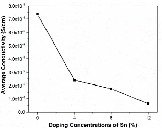
The present work demonstrates the Characterization of pure CuO and Sn doped CuO thin films after optimizing the substrate temperature, mole concentration and volume of the solution of copper oxide (CuO) thin films prepared by jet nebulizer spray pyrolysis (JNSP) technique. Such prepared CuO and SnCuO thin films were characterized by XRD, SEM, EDX, UV-vis and I-V. From XRD investigation the mole concentration, volume level and substrate temperature of the prepared CuO films were fixed as 0.20M, 5 ml & 4500C respectively and optimized for P-N diode application. The XRD pattern of the optimized CuO and SnCuO film reveals monoclinic structure. The surface morphological variations and elemental present were confirmed by SEM and EDX analysis. The optical properties were recorded by UV-vis spectrum and the minimum band gap value is observed as 1.63 eV for 450°C substrate temperature. The maximum conductivity value of the prepared CuO is recorded as 7.4 x 10⁻⁹ S/cm from I-V characterization .Using J-V, the diode parameters of p-CuO/n-Si prepared at 450°C with 0.2 M and 5 ml were measured in dark and under illumination. The ideality factor (n) and barrier height (b) values of p-CuO/n-Si diode are 6.2 and 0.80 eV in dark and 4.6 and 0.81 eV under
illumination.
Also SnCuOthin films and p-SnCuO/n-Si diodes were prepared for different doping concentration of Sn from 0 to 12 wt.% at 450 °C using JNSP technique, which is a promising method to obtain an uniform thin film. From UV-vis spectra, pure CuO film shows the minimum absorbance with the minimum band gap energy value of 1.62 eV. XRD results exhibited the monoclinic structure. Crystallite size of SnCuO films decreases from 48.18 to 39.25 nm with increase in Sndopent. From the SEM, the increasing of Sn doping changes the different surface morphologies of the prepared samples. The EDX spectra have proved the presence of the elements of Sn, Cu and O in the prepared films. From I-V, the prepared films expose decrease in conductivity from 7.35892 x 10⁻⁹ to 6.27867 x 10⁻¹⁰ S/cm owing to increasing the concentrations of Sn. From diode characterization of p-SnCuO/n-Si diodes in darkness and under light illumination, n and b values were
II.
EXPERIMENTAL PROCEDURES
2.1 SnCuO films and diode fabricationThe precursor materials of copper (II) acetate monohydrate (C4H6CuO4. H2O) and tin chloride
(SnCl4.5H2O) were purchased from Sigma-Aldrich. The precursor solution of copper (II) acetate (0.20 M) and
SnCl4.5H2O (0, 4,8 and 12 wt. %) was dissolved in deionized water and stirred well for an hour at ambient
temperature. For film preparations, the prepared solution (5 ml) was taken and sprayed on the well-cleaned glass substrates (2 x 2.5 cm size) at the substrate temperature of 450°C in the air. To fabricate a quality diode, the first step is silicon wafer cleaning because there may be several impurities including dust, grease, metallic impurities and organic residues on the surface. The steps of cleaning process have been reported [35]. From the precursor solution, 2.5 ml of solution was sprayed on the n-type silicon wafer (1 x 1 cm size) at 450°C. After the Sndoped CuO film was coated on Si wafer, the silver (Ag) paste (ELTECK Corporation) was used to make the better ohmic contact at both surfaces. To get a gel form, the Ag paste was completely mixed with isoamyl acetate and applied to both sides of the p-SnCuO/n-Si diode. The device was then dried at room temperature for 5 h. A good adhesion, high electrical conductivity, low sheet resistance (>0.02 Ω/cm) and good solder ability properties of Ag paste are playing the main role in diodes. The experimental setup of the JNSP technique was already mentioned in previous reports [34,35].
2.2 Characterization techniques
Structural studies were carried out using the X-ray diffractometer (XRD, XPERT-PRO) with CuKα1 radiation of wavelength 1.5406 Å at a generator setting of 30 mA and 40 KV in the 2θ range from 20 to 70°. The surface morphology of the prepared thin films was investigated by the scanning electron microscope (JEOL JEM 2100). Elemental presence was confirmed by EDX (QUANTA FEG 250). The optical studies were examined by the UV-Visible spectrophotometer (Perkin Elmer Lambda 35) in the wavelength range from 300 to 900 nm. The DC electrical conductivity and diode studies of the pure and Sn doped CuO films were measured by the Keithley Electrometer 6517-B.
III.
RESULTS AND DISCUSSION
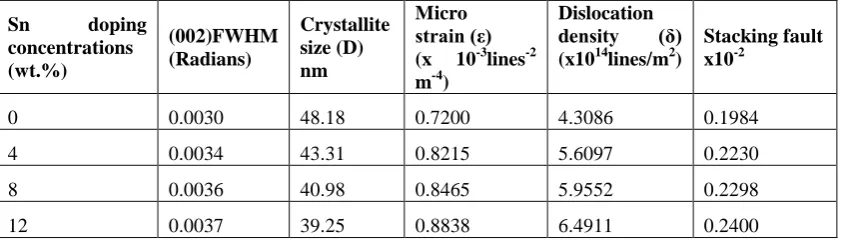
3.1. XRD patternThe XRD patterns of the copper oxide and Sn doped copper oxide at different dopent concentrations (0 to 12 % by a step of 4 %) deposited on glass substrate at 450℃ is shown in Fig. 1.It is seen that all the films are polycrystalline in nature having monoclinic crystal structure with a preferential oriented growth along (0 0 2) plane (JCPDS Card no. 45-0937).The other peak like (1 1 1) also seen substantially with low intensities. From the Fig. 1,it is observed that the intensity of (0 0 2) peak and FWHM decrease as Sn doping concentration increases.
Table 1 shows the microstructural properties of the crystallite size (D) [20,21], dislocation density (δ), microstrain (ε) and stacking fault (SF) values for the preferred orientation of (0 0 2) plane of the WMoO3 thin
films and the values are calculated using the following equations (1-4) [7,12,13],
D = kλ
βcosθ (1)
ε= βcosθ
4 (2)
δ= 1
D2 (3)
SF = 2π2
45(3tanθ)1/2 β (4)
Fig. 1. XRD patterns of pure CuO and different doping concentrations of Sn doped CuO thin films
Table 1. The microstructural properties of SnCuO thin films at different doping concentrations of Sn
Sn doping
concentrations (wt.%)
(002)FWHM (Radians)
Crystallite size (D) nm
Micro strain (ε) (x 10-3lines-2 m-4)
Dislocation density (δ) (x1014lines/m2)
Stacking fault x10-2
0 0.0030 48.18 0.7200 4.3086 0.1984
4 0.0034 43.31 0.8215 5.6097 0.2230
8 0.0036 40.98 0.8465 5.9552 0.2298
12 0.0037 39.25 0.8838 6.4911 0.2400
The microstructural parameters such as crystallite size, microstrain and dislocation density values were calculated from XRD data and the values are presented inTable 1. The variations of crystallite size, microstrain and dislocation density are shown in Fig 2a&b,respectively.The variation of crystallite size is determined for the CuO and Sn doped CuO films using the FWHM along (0 0 2) plane. Crystallite size of SnCuO films decreases from 48.18 to39.25 nm with increase in Sndopent as shown in Table 1 [5]. V. Madhavi et al. [40] observed that decreasing of crystallite size and increasing of strain by increasing of Mo doping concentration on WO3. K.J.
Fig. 2. The microstructural properties of (a) microstrain and crystallite size and (b) dislocation density for pure CuO and different doping concentrations of Sn doped CuO thin films
3.2.SEM analysis
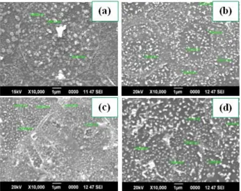
The surface morphology of pure CuO andSndoped CuO films are shown in Fig. 3.It shows a large variety of nanostructures randomly distributed over the film surface. Fig. 3a shows undoped CuO particles which exhibits the formation of spherical shapes of different sizes aligned horizontaly and distributed over the film surface. The types of nanostructures have potential use as gas sensor, dye synthesized solar cells and energy storage device etc.
Fig. 3b shows that there is a change in surface morphology of CuO films due to presence of Sn and ovel shaped grains of about 100 nm. It also shows that increase ofSn doping, the shape of the grains arespherical and size become small as shown in Fig. 3c. Film deposited with the Sn ratio 12% has a randomly oriented grains of approximately 130 nm in size(Fig. 4d).Therefore, Sn doping concentrations on CuO thin films strongly disturb the surface morphology in this present study of JNSP technique.
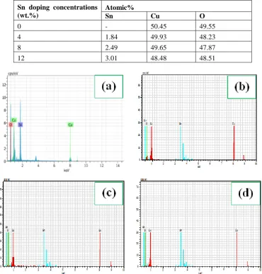
3.3.EDX spectra
Elemental analysis is useful to identify materials and contaminants, as well as estimating their relative concentrations on the surface of the specimen. The EDAX spectrum of pureCuO and SnCuO thin films are shown in Fig.4a-d.The EDX spectra reveals that the films contain the Sn, Cu and O as expected. The compositional analysis of pure CuO film indicates that the atomic percentage ratio of Cu:O and Sn:Cu:O are shown in Table 2.
Table 2. Atomic percentage of CuO and Sn doped CuO thin films
Sn doping concentrations (wt.%)
Atomic%
Sn Cu O
0 - 50.45 49.55
4 1.84 49.93 48.23
8 2.49 49.65 47.87
12 3.01 48.48 48.51
Fig. 4.EDX spectra of (a) pure CuO, (b) 4, (c) 8 and (d) 12 wt.% of doping concentrations of Sn doped CuO thin films
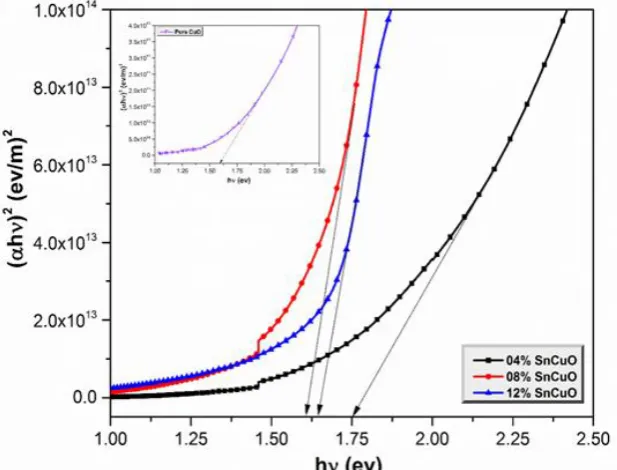
3.4.UV-vis results
Fig. 5. The absorbance spectrum of pure CuO (inset figure) and SnCuO thin filmsfor different doping concentrations of Sn
The UV-visspectrarevealsthevariations in absorbance for increasing the doping concentrations of Sn. The variation of absorbance observed in the present study might be attributed to the possible light scattering at the grain boundaries and considerable thickness of the films. From the UV-vis results, the optical band gap values of the deposited films were evaluated. It can be seen that the plots are linear in the region of strong absorption i.e. near the fundamental absorption edge. In order to determine the optical band gap energy Eg from
the absorption spectra we used the variation of the absorption coefficient (α) with photon energy, using the relation (5),
αhν= A hν− Eg
1
2 (5)
whereEgis the optical band gap of the films and A is a constant. Fig. 6 shows the plots of (αhν)2 versus (hν) for
The Fig.6 shows the variation of band gap values for pure CuO and Sn doped CuO films from 1.59 to 1.75 eV with increasing Sn doping from 0 to 12wt.%. This variation in band gap with the increasing Sn concentration might be explained in terms of electron concentration dependence of band gap shift in the SndopedCuO films.
3.5. Electrical characterization 3.5.1.DCconductivity
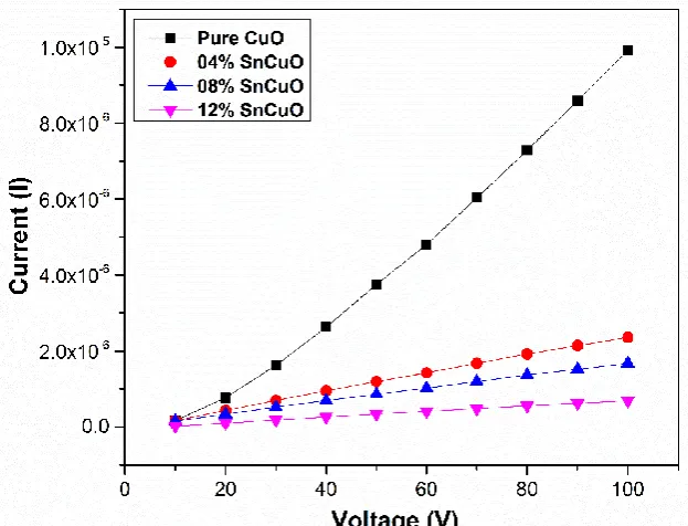
The electrical conductivity was carried out using the Keithley electrometer 6517B two probe setup. The current flow through the film for the constant voltage of 10 - 100 V was studied. The measurement gives the ohmic behavior of the CuO and SnCuO films at room temperature shown as a function of Sn doping concentrations from 0 to 12 wt% in Fig. 7. The given equation (6) is used to calculate the conductivity () for WMoO3 films [12,7],
= I
V × d
A (6)
where I, V, d and A are mentioned as the current, applied voltage, inter-probe distance and cross-sectional area of the film.
Fig. 7.I-V results of pure CuO and Sn doped CuO thin filmsfor different doping concentrations of Sn
Fig. 8.Average conductivity of pure CuO and Sn doped CuO thin filmsfor different doping concentrations of Sn
3.5.2 The diode characterization of p-SnCuO/n-Si
The p-SnCuO/n-Si junction diodes were fabricated for varying Sn doping concentrations of 0, 4, 8 and 12 wt.% by JNSP technique. The forward to reverse bias current of the prepared diodes is measured for the corresponding applied voltage from -4 to +4 V in darkness and under illumination as displayed in Fig. 9a-d.Fig. 10a-d elucidates the semi-logarithmic plots of ln J versus V. A good rectification behavior is observed for the p-SnCuO/n-Si diodes.
The current density (J) of the p-SnCuO/n-Si diodes is calculated using the thermionic emission theory (TE) as follows (7) [25],
J = J0 exp qV
nKT − 1 (7)
where Jo, q, V, n, K and Tare referred as reverse saturation current density, electron charge, applied voltage,
ideality factor, Boltzmann constant and absolute temperature.
The n value of the diode is determined by the slope and the intercept of the semi-logarithmic forward bias of J-V plot for V ≥ 3kT/q using equation (7).
The b and n values are calculated by the following equations (8,9) [26] and listed in Table 3, n = q
KT dV
d ln J (8)
b= KT
q ln A∗T2
J0 (9)
where A* is denoted as Richardson constant.
Using J-V method, the obtained n values of p-SnCuO/n-Si diodes at different doping concentrations of Sn from 0 to 12 wt.% have changed from 6.2 to 3.2 in darkness and 4.6 to 1.9 under the illumination (Table 3). The n value mainly depends on the conversion efficiency of n-Si and the absorption of p-SnCuOthin film layer including its thickness [27]. The n value is equal to one for an ideal P-N diode but, the observed n values are more than an ideal P-N diode in this present study. The p-SnCuO/n-Si junctiondiodes are representing a non-ideal behavior that may be owing to the SiO2 interfacial thin native layer presence between the electrode and Si
wafer or recombination of charge in the space charge region [26,28] and barrier inhomogeneities[29].
Table 3. Diode parameters of n and b forp-SnCuO/n-Si junction diodes for different doping concentrations of
Fig. 7. I-V characterizationof p-SnCuO/n-Si junction diodes for (a) 0, (b) 4, (c) 8 and (d) 12 wt.% of doping concentrations of Sn
IV.
CONCLUSION
The SnCuOthin films and p-SnCuO/n-Si diodes were prepared for different doping concentration of Sn from 0 to 12 wt.% at 450 °C using JNSPtechnique, which is a promising method to obtain an uniform thin film. From UV-vis spectra, pure CuO film shows the minimum absorbance with the minimum band gap energy value of 1.59 eV. XRD results exhibited the monoclinic structure. Crystallite size of SnCuO films decreases from 48.18 to 39.25 nm with increase in Sndopent. From the SEM, the increasing of Sn doping changes the different surface morphologies of the prepared samples. The EDX spectra have proved the presence of the elements of Sn, Cu and O in the prepared films. From I-V, the prepared films expose decrease in conductivity from 7.35892 x 10⁻⁹ to 6.27867 x 10⁻¹⁰ S/cm owing to increasing the concentrations of Sn. From diode characterization ofp-SnCuO/n-Si diodes in darkness and under light illumination, n and b values were calculated. The photo
conducting nature of the prepared diodes endorses the application of photodetectors.