234 |
P a g e
LOW POWER AREA EFFICIENT CARRY SELECT
ADDER USING TSPC D-FLIP FLOP
Manjunath.R
1, Nagabhushan.M
2, Shruthi Gatade
3 1,2,3ECE, MSRIT, (India)
ABSTRACT
In the emerging field of electronics, consumers demand faster devices with less area and low power
consumption. In all the data processing processors, adder plays an important role. CSLA is considered to be the
best adder design for many data processing processors. Conventional CSLA uses a pair of ripple carry adder,
one with Cin=0 and other with Cin=1. It consumes a lot of chip real estate because of use of two ripple carry
adders in the design. In spite of having two RCAs, only one RCA with Cin =0 is used and the result of which is
given to add one circuit (BEC) or the D-latch to obtain the results of Cin=1. Later the MUX selects the
appropriate output according to the carry out of the previous state. Efficient adder is adder is used along with
the proposed D-latch. The output of RCA with cin=0 is taken and given as input to BEC , which gives the results
which is same as RCA with Cin=1. In D-latch circuit when clock is ‘0’ RCA gives the output to the D-latch and
when clock changes from ‘0’ to ‘1’ the output is passed to the multiplexer and the present output of RCA which
is same as RCA with Cin=1 is also given to MUX, according to the previous carry, the output is selected.
In this paper a new modified D-FF is used which gives a better result when compared to the normal FF in terms
of power and uses one less transistor than the previous TSPC FF.
Keywords
:
BEC-binary to excess one code converter, Cin-carry input, CSLA-carry select adder,
FF-flip flop, RCA–ripple carry adder, TSPC-true single phase clock.
I. INTRODUCTION
VLSI system with low power consumption and less area are used in many electronic devices. Larger the
complexity, the DSP requires the larger number of address. Efficient adder design thereby improves DSP
performance in turn makes the devices work faster. CPD is the main concern in the RCA. Different adder
designs are suggested to overcome CPD such as Carry Select adder and Carry Look-ahead adder. Designing the
area and power efficient logic systems are the area of interest for the research in VLSI system design. Carry
select adders are faster adders because the summation results due to the area available before the carry
generated by the previous stages of adders. There is a single multiplexer delay will to select the appropriate
output.
In Conventional carry select adder, two ripple carry adders are used in tandem with multiplexer. One RCA with
carry input as ‘0’ while the other as carry input ‘1’. The multiplexer selects one of the output from RCA’s in
accordance to the select input, which is cascaded from the carry output of the previous stage. Hence we can
obtain the computational output just with a single multiplexer delay. Thereby reducing the CPD as compared to
RCA, but with the trade off with respect the area as it uses two RCAs.
235 |
P a g e
a add one circuit. The output of RCA with Cin=0 is given to add-one circuit which gives the results of Cin=1.
The output of add-one circuit and the RCA is input to multiplexers; the appropriate output is selected according
to the carry of the previous stage which acts as the select line to the multiplexer. As add-one circuit requires less
number of gates and gate delay, when compared to RCA, this reduces the area of the delay. This architecture to
obtains a better result in terms of area and delay as compared to conventional based CSLA.
The Boolean expression for 4-bit BEC is as shown below:
P0= ~ x0
P1= x0^x1
P2= x2^(x0&x1)
P3= x3^(x0&x1&x2)
Instead of using two RCA’s in the design of CSLA, a single RCA is used and other RCA is replaced with
D-Flip Flop. The RCA and D-D-Flip Flop are triggered by the same clock signal. When clock is in the state‘0’ the
RCA generates the output and it is stored in D-Flip Flop, the result is same as RCA with Cin=0. However, when
the clock changes from negative to positive, the output of D-Flip Flop is input to multiplexer along with the
output of the RCA. This design is more advantageous in terms of area and power when compared to add-one
and Conventional method.
In this paper, we have used an efficient adder which is rid of all the redundant logic terms which is
described[Base paper] along with the new proposed design of TSPC D-Flip Flop which uses fewer number of
transistor when compared to the normal TSPC D-Flip Flop.
II. AREA AND DELAY CALCULATION OF RCA
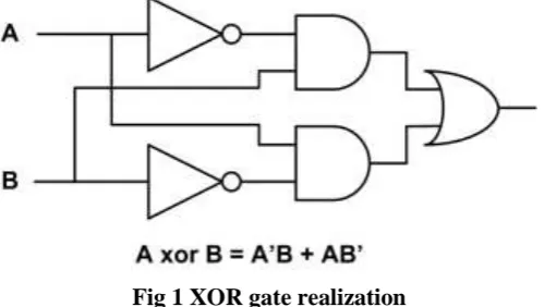
To calculate the area and delay, the logic expression of adders are realized in AOI implementation. Considering
the unit delay and unit area of the AOI gates, realizing the XOR gate, is shown in fig 1
Fig 1 XOR gate realization
The maximum delay is obtained by adding all the gates in the largest path. Table 1 shows the area and delay of
XOR, adder and MUX[2:1]
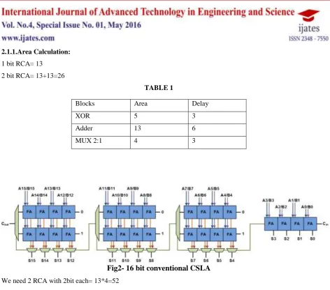
2.1.Conventional CSLA
Realizing a conventional CSLA using AOI logic, Table 2 shows the area and delay of 16 bit CSLA
236 |
P a g e
2.1.1.Area Calculation:
1 bit RCA= 13
2 bit RCA= 13+13=26
TABLE 1
Fig2- 16 bit conventional CSLA
We need 2 RCA with 2bit each= 13*4=52
One multiplier is 6:3, which is 3 times of 2:1
2:1 MUX= 4
Therefore Total gate area= RCA’s + MUX= 52+12= 64
2.2.BEC based CSLA
As shown in the expression below, to replace the second RCA, and realizing its AOI logic, we obtain less area
and delay. Considering Block2 which is of 2 bit with one multiplexer.fig shows the realization of binary to
excess one code.
Fig3: Binary to excess one code circuit.
Below shows the expressions for binary add one:
P0= ~ x0
P1= x0^x1
Blocks Area Delay
XOR 5 3
Adder 13 6
237 |
P a g e
P2= x2^(x0&x1)
P3= x3^(x0&x1&x2)
Area can still be reduced by using half adder in the design when carry input is ‘0’ instead of full adder, which
would save the area by about 7 units in all the stages. Therefore the reduced area count is tabulated in Table 2
and Table 3
Fig4: 8-bit CSLA using BEC
TABLE 2
Conventional based CSLA’s area count
Stage Area
Stage 1 57
Stage 2 87
Stage 3 117
Stage 4 147
TABLE 3
BEC based CSLA’s area count
Stage Area
Stage 1 43
Stage 2 61
Stage 3 84
Stage 4 107
2.3TSPC D-Flip Flop based CSLA
Replacing the second RCA with D-Flip Flop will help in reducing the area when compared to both conventional
238 |
P a g e
Fig5: Proposed design of carry select adder
2.3.1Area calculation of D-Flip Flop based CSLA
TABLE 4
Realizing logic gates in transistor level we obtain
Gates Transistor required
AND 6
OR 6
XOR 22
NOT 4
Full adder 74
D-Flip Flop 11
In the paper, A new TSPC D-FF is proposed , which has fewer number of transistors when compared to the
previous TSPC and also consume less power when compared to earlier version. In the second stage of TSPC
the PMOS transistor has been eliminated. The output of the first stage drives the second stage but in the
previous design clock was driving the second stage. This requires one less transistor than the normal TSPC.
Using the proposed type TSPC we can obtain less area and less power in turn results in efficient adder.fig5 and
fig6 shows the schematic of TSPC D-FF and output of TSPC based CSLA respectively.
239 |
P a g e
Fig7:Output waveform of TSPC based CSLA
III. RESULTS
The proposed design of CSLA is good in power and area. We have considered 1.8v as the input and tabulated
the results for power. It was observed that the proposed design has the better performance when compared to the
previous design. Figure 7 shows the output waveform of 16 bit. We have designed a CSLA for 4-bit,8-bit and
16-bit for conventional ,BEC based and for the proposed TSPC based CSLA. It is clear that we have reduce the
area and the power for the proposed design. Power output of all the designs are calculated and tabulated in table
5.Our proposed design performs an addition function which is more efficient than the previous CSLA design.
The power results of various adders design are tabulated in table 5.Spectre simulator is used and virtuoso tools is
used for the entire design.
IV. CONCLUSION
In this paper, the conventional BEC based and proposed carry select adder using TSPC is designed using 90nm
technology in Cadence Analog Design. The carry input block is replaced with TSPC D-FF. The proposed
design of the carry select adder using TSPC is better in terms of area and power when compared to
conventional and BEC based CSLA. The results for power of 4bit, 8bit and 16bit is tabulated and is concurred
that the proposed TSPC based CSLA is more efficient when compared to earlier CSLA.
Table 5
Comparison of power in different adder design
4-Bit 8-Bit 16-Bit
Conventional CSLA 303.9mW 59640mW 71990mW
BEC based CSLA 268.2mW 33370mW 68230mW
TSPC D-FF based CSLA 1.91mW 5.72mW 7.951mW
REFERENCES
[1]. Basant Kumar Mohanty, ―Area-Delay Power Efficient Carry Select Adder‖,IEEE Transactions On Circuits
240 |
P a g e
[2]. He, Y. Chang, C. H. and Gu, J. ―An Area Efficient 64Bit Square Root Carry-Select Adder for Low Power
Applications‖, in Proc. IEEE Int. Symp. Circuits Syst., vol.4, pp. 4082–4085, 2005.
[3] J. M. Rabaey, Digital Integrated Circuits,‖ IEEE Trans. on VLSI Systems, 2003.
[4] Ramkumar, B. and Harish M Kittur, (2011) ‗Low Power and Area Efficient Carry Select Adder‘, IEEE