IMPLEMENTATION OF LOW TRANSITION LFSR
TEST PATTERN FOR LOGIC BIST
Afshan Jabeen¹, Bobbili Saikumar², G.Sai Adithya
3 1Assistant Professor,
2,3B.Tech Student, Dept. of Electronics and Communication,
Sphoorthy Engineering College
ABSTRACT
A Low Transition LFSR(LT-LFSR) designed by modifying Linear Feedback Shift Register is proposed to
produce low power test vectors which are given to Circuit under Test (CUT) to reduce the power consumption
by CUT. This technique of generating low power test patterns is performed by increasing the co-relativity
between the consecutive vectors by reducing the number of bit flips between successive test patterns. The
proposed architecture increases the correlation among the vectors generated by LT-LFSR with negligible
impact on test length. Verilog HDL is used as HDL language. The results were analysed using Xilinx for
simulation and synthesis. The experimental result shows overall reduction in the total power consumption of the
BIST circuitry.
Keywords: BIST; CUT; LFSR; TPG; TEST VECTOR; VERILOG
I.
INTRODUCTION
The technique of designing additional hardware and software feature into integrated circuits is known as Built in self test (BIST). The fast-rising costs of ATE testing and the growing complexity of circuits are main drivers for the widespread development of BIST technique. Such complex devices require mixed signal testers that possess special digital and analog testing. The Logical Built-in Self Test (BIST) is designed for testing random logic, typically employs a Pseudo Random Pattern Generator(PRPG) to generate input patterns that are applied to the device’s internal scan chain, and Multiple Input Signature Register(MISR) is used for obtaining the response of the device to these test input patterns. An undesirable MISR output indicates that defect is present in the device. With the rising costs of external electrical testing and increasing intricacy of devices BIST is becoming an alternative solution. Better BIST techniques are developed and this approach will find the greater use in a wide variety of circumstances. BIST will someday be the chosen mode of testing and the proponents are positive instead of being merely an alternating to external ATE testing as it is today.
architecture, an analysis of power dissipation for testing is presented and ISCAS Benchmark Circuit C6288 is discussed briefly, which is the circuit under test (CUT) to verify the potency of the proposed method. In section IV proposed method which is a low power test pattern generator is discussed in detailed. In Section V, the implementations details are discussed. Section VI outlines the conclusion.
II.
PRIOR WORK
Various techniques are available to reduce the switching activities of test vectors; with the help of these methods the power in test mode can be reduced. By using linear feedback shift register (LFSR) combination with SIC generators, Bo YE Tian-wang Li proposed LSA-TPG a Novel BIST Scheme for Low Power Testing[1]. Patrick Girard proposed a modified clock scheme in which only half of the D flip-flops works, therefore only half of the test vectors are switched [7]. S.K. Gupta proposed a BIST TPG for low switching activity was in which there is d-times clock frequency between slow LFSR and normal LFSR and thus the test pattern generated by original LFSR is rearranged to reduce the switch frequency. LT-TPG is proposed to reduce consumption of power by circuit during test [6]. Compared to traditional linear feedback shift register (LFSR) the above said techniques can reduce the average power. By using single input change pattern generators a desirable low power can be achieved. The combination of LFSR and scan shift register is used to generate random single input change sequences a proposed method which is [9 &10]. In [11 &12], In between two adjustment vectors generated by LFSR it is proposed that (2m-1) single input change test vectors can be inserted, m is length of LFSR. In [5], it is proposed that 2m single input changing data inputs is inserted in between two neighboring seeds, power consumptions is reduced by using the above methods, still the switching activities will be large when clock frequency is high .This paper proposed a new technique with negligible clock frequency with compared to existing method switching activity.
III.
BACKGROUND WORK
Power consumption in CMOS circuits is classified into static and dynamic. Static power dissipation is due to leakage current or other current drawn continuously from the power supply. Dynamic dissipation is due to short circuit current which is due to the transistors remaining in on state for small period of time and the charging and discharging of load capacitance during output switching. The most supreme source of power consumption in the present CMOS technology is dynamic power; this may also vary for upcoming improvements of high scaled CMOS circuits. The generalized expression for the switching power dissipation of a CMOS VLSI circuits can be calculated from the given equation [1].
P = αT Cload V2dd fclk (1)
αT is given by the switching activity. Cload is represented by the total load capacitance. vdd is given as supply
voltage and fdd is represented as operating frequency. The dynamic power consumed is directly proportional to
the switching activity factor of the gate αT. By controlling the switching activity factor of the gate and the load capacitance the power dissipation during testing can be reduced.
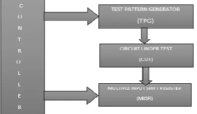
BIST architecture is mainly used for testing in VLSI circuit design. The primary goal of BIST is to reduce the power dissipation without degrading the overall system performance and fault coverage [3].To reduce the costs of external circuit testing BIST has now become an alternative solution. As more as better BIST techniques are developed. The BIST approach promises to find greater use in a wide variety of circumstances
If a fault is found, a part of the circuit (having the fault) is replaced with a corresponding redundant circuit part
(by re-adjusting connections). Testing a circuit each and every time before they startup, is called
Built-In-Self-Test. Off-line testing and BIST is basically same as using ATE where the test pattern generator and the test
response analyzer are on-chip circuitry instead of equipments. By replacing circuitry by equipments, so the
compressed implementations of test pattern generator and response analyzer are to be designed. The basic
architecture of BIST is shown in Figure 1. B Design of c6288 circuit
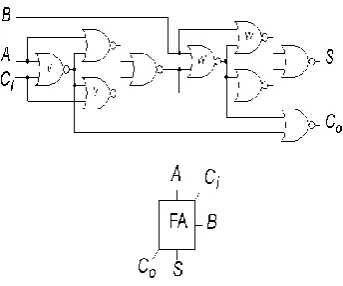
We used c6288 as a Circuit under Test (CUT). c6288 is 16*16 bit multiplier with binary and BCD arithmetic, logic and shift operations. It has 32 inputs; 32 outputs; 2406 gates form 240 full and half adder cells arranged in a 15x16 matrix. The c6288 benchmark, whose multiplication function was previously known and represents a much larger gate-level circuit that also has a concise functional description. Figure 2 shows 2406 gates form 240 full and half adder cells arranged in a 15x16 matrix.
Fig. 1.Bist Architecture
The 15 top-row half adders lack the C_i input; each has two inverters at locations V. The single half adder in the bottom row lacks the B input, thereby acquiring two inverters at locations
Fig. 3. ISCAS-85 C6288 16x16 Multiplier Full Adder Module
C. Standard Ex-OR LFSR
The most widely used test pattern generator because of its small circuit area and excellent random characteristics is the low power LFSR. The standard LFSR consists of n-D flip-flops and a selected number of exclusive-OR (XOR) gates where XOR gates are placed on the external feedback path, it is also referred to as an external-XOR LFSR. A primitive polynomial of degree n over Galois field GF(2), p(x), as a polynomial that divides 1+ xT, but not 1+ xi, for any integer i < T, where T = 2n −1. So we are using a primitive polynomial based external XOR LFSR to generate the test patterns or test sequences for n =50.
D. Generating Test Vectors using LT LFSR
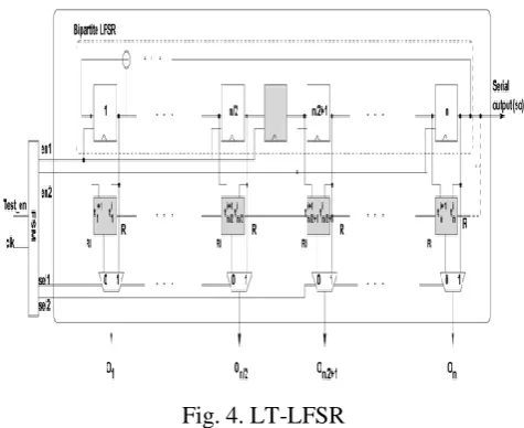
For low-power BIST we combine two techniques of pattern generation Random Injection (RI) method and Bipartite LFSR. The new low transition LFSR (LT-LFSR) generates three intermediate patterns (Ti1,Ti2 and Ti3) between Ti and Ti+1 .To create LT- LFSR we embed these two techniques into a bit-sliced LFSR architecture Compared to having only one of the R-Injection and Bipartite LFSR techniques in a LFSR this provides more power reduction. This may seem to prolong test session by a factor of 4. However, In terms of fault detection. due to high randomness of the inserted patterns many of the intermediate patterns can do as good as patterns generated by a LFSR In fact, in Section VI we show that the overall power consumption of LT-LFSR is quite less when compared to conventional LFSR.
An LFSR is divided into two halves by applying two complementary (non overlapping) enable signals. When one half is idle mode the other half is working. A flip-flop with enable is included in the LFSR. The Fig. 4 shows the architecture of the Bipartite LFSR. It is used to generate intermediate pattern Ti1, en1 and en2 are two non overlapping enable signals.
LT-LFSR reduces the transitions between consecutive patterns that can be used for test-per-clock architecture. The generated patterns can be used for test-per-scan architecture to feed scan chains with a lower number of transitions. The LT-LFSR is shown in Figure. 4
Even though the basic idea of Bipartite LFSR is not new, the architecture of LT-LFSR is much more efficient in terms of randomness of patterns and power.
Fig. 4.
LT-LFSR
In [13], the authors used two n-bit random pattern generators and n (2x1) multiplexers, but we only add one flip-flop to an n-bit LFSR. The area overhead of Bipartite LFSR is much lower than LPATPG. They reduce the CUT and clock tree power consumption when an n-bit LFSR is divided into two n=2-bit. It reduces the randomness property of the LFSR due to dividing it into two smaller LFSR and it also requires generating and distributing two non overlapping clocks (with half frequency), which in turn increases the area overhead of Bipartite LFSR is much lower than LPATPG is the main drawback.. In [14], an n-bit LFSR is divided into two n/2-bit LFSRs, which together reduce the CUT and clock tree power consumption.
The technique is that it reduces the randomness property of the LFSR due to dividing it into two smaller LFSR and it also requires generating and distributing two non overlapping clocks (with half frequency), which in turn increases the area overhead. The Bipartite LFSR keeps the randomness property of the n-bit LFSR intact and it also reduces the power consumption of Bipartite LFSR compared to LFSR because, in each period of the clock, half of the LFSR is in idle mode.
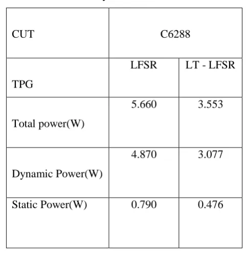
IV. RESULTS
The comparison results explained in table I give the synthesis report of Power consumed by ISCAS’85 benchmark circuit c6288. Standard LFSR and LT-LFSR are used in top module to extract various parameters. The Power consumption during testing i.e total power, Dynamic power and Static power are given in W.
Table 5.1 Synthesis of LT LFSR
CUT
C6288
TPG
LFSR
LT - LFSR
Total power(W)
5.660
3.553
Dynamic Power(W)
4.870
3.077
Static Power(W)
0.790
0.476
V CONCLUSION
A LT-LFSR is a low power test pattern generator which has been designed and implemented using XILINX tool. This method adequately and effectively reduces the switching correlations between the test pattern. It greatly reduces the power consumption during testing mode with minimum number of switching correlations and gives better power reduction compared to the existing method. Hence the proposed effective low power Test Pattern Generator consumes less power and also reduces the dynamic power consumed by CUT than compared to standard LFSR.
REFERENCES
[1] “A Novel BIST Scheme for Low Power Testing” by Bo YE Tian-wang Li, CHINA, 2010 IEEE.
[2] Balwinder Singh, Arun khosla and Sukhleen Bindra “Power Optimization of linear feedback shift register(LFSR) for low power BIST”, IEEE international advance computing conference, Patiala, India 6-7 March 2009.
[3] A.Kavitha,G.Seetharaman,T.N.Prabhakar and Shrinithi “Design of Low Power TPG using LP/LFSR”, 3rd IEEE Conference on international conference on intelligent systems modeling and simulation 2012. [4] Mohammad Tehranipoor, Mehrdad Nourani, Nisar Ahmed, “Low Transition LFSR for BIST Based
[5] S.C. Lei, X.Y.Hou ,Z.B.Shao and F.Liang,” A class of SIC circuits: theory and application in BIST design,” IEEE trans. circuits syst. II, vol.55,no.2,pp.161-165,Feb.2008.
[6]. DS-LFSR : A BIST TPG for Low Switching Activity. Seongmoon Wang, Sandeep K. Gupta. IEEE transactions on Computer-Aided Design of Integrated Circuits and Systems. Vol.21,No 7 July 2002. [7].Low Power Testing of VLSI Circuits: Problems and Solutions by Patrick Gigard, member, IEEE.
[8]. N. Ahmed, M. Tehranipoor, and M. Nourani, “Low Power Pattern Generation for BIST Architecture,” Proc. Int’l Symp. Circuits and Systems, vol. 2, pp. 689-692, 2004.
[9]. M. Tehranipoor, M. Nourani, and N. Ahmed, “Low Transition LFSR for BIST-Based Applications,” Proc. IEEE 14th Asian Test Symp, 2005.
[10]. F.Corno, M.Rebaudengo, M.Sonza Reorda, “A Test Pattern Generation Methodology for Low Power Consumption”, pp.1-5, 2008.
[11]. Tiwari, Honey Durga, et al., "Multiplier design based on ancient Indian Vedic Mathematics,” Int. SoC Design Conf., 2008, vol. 2. IEEE Proc., pp. II-65 - II-68.
[12]. N. Basturkmen, S. Reddy, and I. Pomeranz, “A Low Power Pseudo-Random BIST Technique,” Proc. 1st International Conference on Computer Design, pp. 468- 473, 2002.
[13]. X. Zhang and K. Roy, “Peak Power Reduction in Low Power BIST,” in Proc. Int. Symp. on Quality Elect. Design (ISQED’01), pp. 425-432, 2001.