Various Methodologies used for 25 Bit Information Data
String Communication through Hamming Code
Brajesh Kumar Gupta
Rajeshwar Lal Dua
M.Tech Scholar Head of Department
Elect. & Comm. Engg. Department Elect. & Comm. Engg. Department Jaipur National University, Jaipur Jaipur National University, Jaipur
ABSTRACT
Till now communication is possible of 7 bit information data string by transmitting 11 bit data string in single frame due to this speed of communication system is very slow. And we can transmit very minimum number of configuration of data string. To increase the speed of communication system and increase the numbers of configuration data string author design some communication system by different methodologies of Hamming code. About all these communication systems all methodologies are discuss here. First, author design communication system to make communication by even parity check method for 25 bit information data string. In second paper, author design communication system to make communication by odd parity check method for 25 bit information data. In third paper, author again design communication system for 25 bit information data string by even parity and odd parity check method by using VHDL by single system. Till now, for 25 bit information data string communication is possible only in simplex mode. So that now author, design 25 bit hamming code transceiver to make communication possible in full duplex mode.
Key word
Hamming code, VHDL code, Xilinx ISE 10.1 simulator, even parity check, odd parity check, transmitter, receiver, transceiver.
1.
HAMMING
CODE
METHODOLOGIES
Hamming code is a linear error-correcting code named after its inventor, Richard Hamming. Hamming codes can detect up to two simultaneous bit errors , and correct single-bit errors; thus, reliable communication is possible when the Hamming distance between the transmitted and received bit patterns is less than or equal to one . By contrast, the simple parity code cannot correct errors, and can only detect an odd number of errors.[5][6][15][16][19][21]
In 1950 Hamming introduced the (7, 4) code. It encodes 4 data bits into 7 bits by adding three parity bits. Hamming (7, 4) can detect and correct single – bit errors. With the addition of overall parity bit, it can also detect (but not correct) double bit errors. Hamming code is an improvement on parity check method. It can correct 1 error bit only[5][6][15][16][19][21] Hamming code method works only two methods (even parity, odd parity) for generating redundancy bit. In hamming code method for generating the number of redundancy bit use formula .The number of redundancy depends on the number of information data bits[1][2][3].
Formula for generating redundancy bit ----
2^ r >= D + r + 1 --- (1)
Here r = number of redundancy bit
D = number of information data bit Calculate the number of number of redundancy bit for 25 bit of input data string by above formula We get 5 redundancy bit required.
1.1
Redundancy
The central concept in detecting or correcting errors is redundancy. To be able to detect or correct errors, we need to send some extra bits with our data. These redundant bits are added by the sender and removed by the receiver. Their presence allows the receiver to detect or correct corrupted bits. The concept of including extra information in the transmission for error detection is a good one. But instead of repeating the entire data stream, a shorter group of bits may be appended to the end of each unit. This technique is called redundancy because the extra bits are redundant to the information. [5][6][15][16][19][21]
1.2
Even check parity method
In even check parity method count the number of one`s at transmitter and receiver side, if number of one`s are odd, add one else add zero[5][6][15][16][19][21]
1.3
Odd parity check method
In odd parity check method count the number of one`s, if number of ones are odd add zero and if number of one`s are even add one. [5][6][15][16][19][21]
2.
30 BIT HAMMING CODE FOR
ERROR
DETECTION
AND
CORRECTION USING VHDL
In this section, Author design communication systems by even parity check method o make communication for 25 bit information data string. To transmit 25 bit information data string need to add minimum 5 redundancy bits according to equation „1‟ to make 30 bit data string for transmission by transmitter at source section. Value of redundancy bits depends on the value of 25 bit information data according to given equation given below....[1][15][16][17][18]
Calculation of these redundancy bit are given below... r (1) = 1,2,4,5,7,9,11,12,14,16,18,20,22,24.
r(2) = 1,3,4,6,7,10,11,13,14,17,18,21,22,25 r(4) = 2,3,4,8,9,10,11,15,16,17,18,23,24,25 r(8) = 5,6,7,8,9,10,11,19,20,21,22,23,24,25 r(16) = 12,13,14,15,16,17,18,19,20,21,22,23,24,25
Here r(1),r(2),r(4),r(8),r(16) redundancy bits and 1,,2,3,4...25 are 25 bit location of 25 bit information data.
Here we use Xilinx ISE 10.1 simulator to simulate this VHDL code. Xilinx ISE 10.1 project navigator window shows the VHDL code written for source section and Xilinx ISE 10.1 simulation window shows simulated VHDL code in timing diagram waveform.[1][8][9]
Fig. 1- VHDL code for 30 bit hamming code transmitter
Fig.2- Xilinx ISE 10.1 simulation window shows input output waveform for transmitter
At destination section, author write VHDL code for find actual 25 bit information data from received 30 bit corrupted data string. .[1][11][12][13]
A receiver of destination section receives 30 bit corrupted data string and checks is there having any error or not by even parity checks method? If any error is occurred receiver generate error bit location by even parity check method. Location of error bit depends on the value of received data string according to given below...
erroradd(1) = 1,3,5,7,11,13,15,17,19,21,23,27,29 erroradd(2)=2,3,6,7,10,11,14,15,18,19,22,23,26,27,30 erroradd(3)=4,5,6,7,12,13,14,15,20,21,22,23,28,29,30 erroradd(4)=8,9,10,11,12,13,14,15,24,25,26,27,28,29,30 erroradd(5)=16,17,18,19,20,21,22,23,24,25,26,27,28, 29, 30
Here erroradd indicate the error bit address and 1, 2, 3, 4 ...30 indicate the received data string bit address.
Here Xilinx ISE 10.1 project navigator window shows VHDL code of receiver for destination section and Xilinx ISE 10.1 simulation window display the simulated results.... .[1][8][9]
Fig. 3 - Xilinx ISE 10.1 project navigator window shows VHDL code for receiver
Fig.4 - Xilinx ISE 10.1 Simulation winodow display input output waveform for 30 bit hamming code receiver
3.
30 BIT HAMMING CODE FOR
ERROR
DETECTION
AND
CORRECTION WITH ODD PARITY
METHOD BY USING VHDL
Here author design communication system by odd parity checks method for error detection and correction. In this paper author want to transmit 25 bit information data string by transmitting 30 bit data string in odd parity method at source section. At destination section we receives 30 bit data string and find actual 25 bit information data by odd parity check method.[2][7][15][19][20][21]
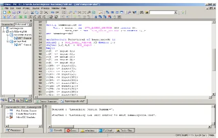
At source section, author written VHDL code for calculating 5 redundancy bits by odd parity check method for 25 bit information data string to make 30 bit encrypted data string for transmission. We use Xilinx ISE 10.1 simulator to simulate VHDL code.[2][ 11][12][13]
Xilinx ISE 10.1 projector navigator window shows the VHDL code for source section and Xilinx ISE 10.1 simulation window display the input – output waveform for source section.[2][18][19]
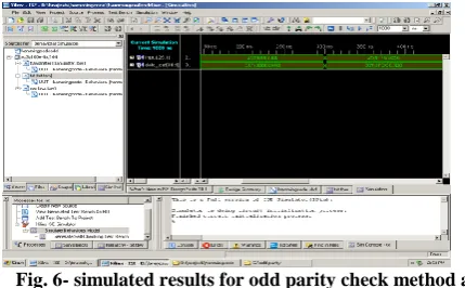
Fig. 6- simulated results for odd parity check method at source section.
At destination section, receiver receives 30 bit data string and check receives 30 bit data string is corrupted or not by odd parity check method? If this received data string is corrupted then receiver fined the error bit location by odd parity check method. For 30 bit data string we need minimum 5 bits to indentifies the address of error bit. After finding the error bit location replace this error bit by „one‟ if the value of error bit is „zero‟ vice-versa. After correction this received 30 bit data string find 25 bit actual information data string from 30 bit correct data string by odd parity check methods.[2][15][16][17][16][17]
Here we have written VHDL code for regenerate 25 bit information data string by odd parity check method for received 30 bit corrupted data string by receiver of destination section.[2][10][11][12][13][14]
Xilinx ISE 10.1 simulator used to simulate VHDL code. Xilinx ISE 10.1 project Navigator window shows the VHDL code for receiver of destination section by odd parity check method. Xilinx ISE 10.1 simulation window display the simulated input output waveform.[2][8][19]
Fig . 7 – VHDL code for receiver section odd parity check method.
Fig. 8 – Simulated results for receiver section of odd parity check method.
4.
30 BIT HAMMING CODE FOR
ERROR
DETECTION
AND
CORRECTION WITH EVEN AND
ODD PARITY CHECK METHOD BY
USING VHDL
Here author design a communication system to make communication possible for 25 bit information data string in even parity or odd parity method. Up to today a single communiction system can be communicate by only even parity method not odd parity method vice – versa. But now author design a single system to be able to generate even parity data string as well as odd parity data string for information data at source section. At destination section receiver receives 30 bit corrupted data string and regenerate 25 bit information data by even parity check method or odd parity check method. Here we use same method for regenerate 25 bit information data string form received 30 bit data string , which we are used to generate 30 bit data string for transmission for 25 bit information data string at source section. Working of this system is devide in two parts they are communication by even paity check method and communication by odd parity check method.[3][5][7][15][16][17][18]
First author use even parity check method to make communication possbile for 25 bit information data string by transmitting 30 bit data string this communication system. Here author author gerenate 5 rdundancy bits by even parity check method for 25 bit information data string to make encrypted 30 bit data string at source section.[1][3][ 16][17][18][20][21]
Here author write VHDL code for even parity check method of source section for 30 bit hamming code error dectection and corrrection with even parity and odd parity check method.[3][10][11][12][13][14]
Author used Xilinx ISE 10.1 simulator to simulate VHDL code for source section. Xilinx ISE 10.1 projector navigator window shows VHDL code for even parity method and Xilinx ISE 10.1 simulation window shows the input output timing waveform for even parity check method at source section for this communication system.[3][8][9]
Fig. 10 simulated results for source section by even parity check method.
At destination secion,author receives 30 bit data tring by receiver of destination section.now receiver checks received data string is corrupted or not by even parity check method for Hamming code with even prity and odd parity check method communication system. If receiver found any error bit is present here, it`s calculate the address of error bit by even parity check method for this communication system. Here 5 bits are required to find the location error bit by even parity check method. After finding the error bit location receiver replace this error bit by „one‟ if error bit is „zero‟ or vice- versa and find actual 30 bit data string. After that receiver of destination regenerate 25 bit information data string from correct 30 bit data string.[3][17][18][19][20][21]
Fig 11 – VHDL code for destination section of even parity check method
Fig. 12- simulated results for destination section of even parity check method
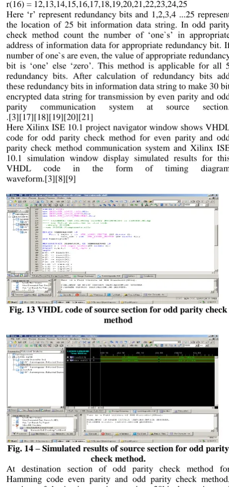
Second author describe the working of odd parity check method for this communication system. At source section of odd parity check method for Hamming code with even parity and odd parity check method, author wish to send 25 bit information data string. To transmit 25 bit information data string needs to add 5 redundancy bits to make 30 bit data string. The value of redundancy bits are depends on the value of 25 bit information data string. .[3][17][18][19][20][21] Calculation of redundancy bits are given below... r (1) = 1,2,4,5,7,9,11,12,14,16,18,20,22,24. r(2) = 1,3,4,6,7,10,11,13,14,17,18,21,22,25 r(4) = 2,3,4,8,9,10,11,15,16,17,18,23,24,25 r(8) = 5,6,7,8,9,10,11,19,20,21,22,23,24,25
r(16) = 12,13,14,15,16,17,18,19,20,21,22,23,24,25
Here „r‟ represent redundancy bits and 1,2,3,4 ...25 represent the location of 25 bit information data string. In odd parity check method count the number of „one`s‟ in appropriate address of information data for appropriate redundancy bit. If number of one`s are even, the value of appropriate redundancy bit is „one‟ else „zero‟. This method is applicable for all 5 redundancy bits. After calculation of redundancy bits add these redundancy bits in information data string to make 30 bit encrypted data string for transmission by even parity and odd parity communication system at source section. .[3][17][18][19][20][21]
Here Xilinx ISE 10.1 project navigator window shows VHDL code for odd parity check method for even parity and odd parity check method communication system and Xilinx ISE 10.1 simulation window display simulated results for this VHDL code in the form of timing diagram waveform.[3][8][9]
Fig. 13 VHDL code of source section for odd parity check method
Fig. 14 – Simulated results of source section for odd parity check method.
At destination section of odd parity check method for Hamming code even parity and odd parity check method, receiver of destination section receives 30bit data string and check is received data is corrupted or not? If receiver find that received data string is corrupted then it find the error bit location by odd parity check method for this communication system. The address of error bit location is depends on the value of received data string. Calculation method of error address bits location is described below.... [3][17][18][19][20][21]
„one‟ else by „one‟. After that receiver find actual information data from intended 30 bit data string.
Here author compact the size of hardware by removing error address bits from input out port of communication system. .[3][17][18][19][20][21]
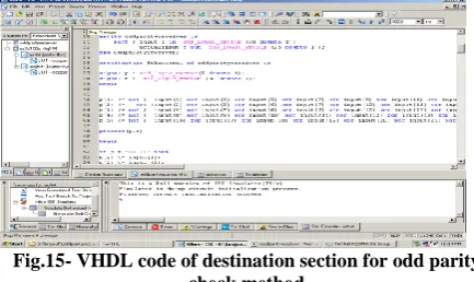
Here author have written VHDL code for destination section of odd parity check method for even parity and odd parity check method communication system. [3][11][12][13][14] Here Xilinx ISE 10.1 simulator is used to simulate VHDL code for destination section of even parity and odd parity check method communication system. Xilinx ISE 10.1 project navigator window display VHDL code of destination section for this communication system and Xilinx ISE 10.1 simulation window display simulated results of this VHDL code in the form of input output waveform.[3][8][9]
Fig.15- VHDL code of destination section for odd parity check method
Fig. 16- Simulated results of destination section for odd
parity check method.
5.
COMMUNICATION
BY
31
BIT
HAMMING CODE TRANSCEIVER
WITH EVEN PARITY AND ODD
PARITY
CHECK
METHOD
BY
USING VHDL
Here author design 31 bit hamming code transceiver to make communication possible in Full Duplex mode. By using this communication system data can transmit or receives by source section as well as destination section.
This system is design to make communication possible in Full Duplex mode for 25 bit information data string by transmit or receiver 31 bit data string at source section as well as destination section.[4][5][6][7][19][20][21]
5.1
Working of transceiver at source
section
At source section of transceiver, transceiver wants to transmit 31 bit encrypted data string to transmit 25 bit information data with 5 redundancy bit and 1 bit for parity check. And it receives 31 bit encrypted data string for finding 25 bit information data which was transmitted by destination section of the transceiver.[4]
.
5.1.1 Working
of
transmitter
of
transceiver at source section
Transmitter of transceiver at source section generates 31 bit data string for 25 bit information data. Here author want to transmit 25 bit information data with even and odd parity check method. To transmit 25 bit information data we need minimum 5 redundancy bit according to equation 1. Here author add one more bit for deciding parity generation method which parity author use to make 31 bit data string. If value of parity decide bit is „one‟ author used even parity method to make 31 bit data string for transmission else use odd parity method. Calculation method of generating redundancy bit depends on the parity method which author used to generate redundancy bits.[4][6][7][8][9]
Suppose these redundancy bits are r(1),r(2),r(4),r(8),r(16). To calculate the redundancy bit, we count the number of ones in appropriate address of information data bit according to given below...
r (1) = 1,2,4,5,7,9,11,12,14,16,18,20,22,24. r(2) = 1,3,4,6,7,10,11,13,14,17,18,21,22,25 r(4) = 2,3,4,8,9,10,11,15,16,17,18,23,24,25 r(8) = 5,6,7,8,9,10,11,19,20,21,22,23,24,25 r(16) = 12,13,14,15,16,17,18,19,20,21,22,23,24,25 .
31 bit encrypted data string hold 25 bit information data string, 5 redundancy bits and one parity decide bit. Block diagram of 31 bit hamming code transceiver at source section given below... [4]
stransmitteroutput
stransmitterinput
Stransmitterevenodd
Fig. 17- Transmitter of source section of transceiver Source
transmitter section of transceiver to generate 31 bit data string for transmission for 25 bit
Here stransmitterinput, stransmitterevenodd and stransmitteroutput pins indicate 25 bit information data string, parity decide bit and 31 bit transmitter output data string.
5.1.2 Working of receiver of transceiver at
source section
At receiver section of transceiver, transceiver receives 31 bit data string which was transmitted by source section; here receiver first check that received 31 bit data string is designed in which parity method for 25 bit information data string at destination section by LSB of received data string. If LSB of received data string is „one‟ means received data is generated by even parity check method else generated by odd parity check method at destination section. After finding the generation method receiver check received data string is corrupted or not by same methodologies? If any error is occurred receiver finds the error bit location using parity check method according to LSB of received data string [4][18][19][20][21]
serroraddress (1) = 1,3,5,7,11,13,15,17,19,21,23,27,29 serroraddress(2)=2,3,6,7,10,11,14,15,18,19,22,23,26,27, 30
serroraddress(3)=4,5,6,7,12,13,14,15,20,21,22,23,28,29 ,30
serroraddress(4)=8,9,10,11,12,13,14,15,24,25,26,27,28, 29,30
serroraddress(5)=16,17,18,19,20,21,22,23,24,25,26,27,28,29,3 0
„serroraddress‟ bits indicate the address of error bit and 1,2,3,4,5,...30 indicate the location of received data string bits. Here sreceiverinput, sreceiveroutput, evenparity and oddparity indicates 31 bit received data string, 25 bit actual information data string, even parity is used to transmit 25 bit information data by transmitting 31 bit data string at destination section and odd parity method used to generate 31 bit data string for 25 bit information data at destination section. Block diagram of receiver of source section. [4][15][16][17][18]
2 5
b i t
s r e c e i v e r o
Fig.18- receiver of transceiver source section
Here author write VHDL code for transmitter and receiver for transceiver of source section. At transmitter section author write VHDL code for generate 5 redundancy bit for 25 bit
information data string with parity decide bit to make 31 bit data string for transmission. [4][10][11][12][13][14]
At receiver section we also written VHDL code for finding error bit location and correcting that error bit by replacing „zero‟ by „one‟ and „one‟ by „zero‟. Author writes VHDL code for regenerate 25 bit information data string from 31 bit correct data string. [4][10][11][12][13][14]
Here author use Xilinx ISE 10.1 simulator to simulate this VHDL code for transmitter and receiver section of transceiver. The VHDL code for transceiver shown in Xilinx ISE 10.1 project navigator window and input output wave form for transceiver at source section shown in Xilinx ISE 10.1 simulation window. [4][8][9]
Xilinx ISE 10.1 project navigator and Xilinx ISE 10.1 simulation window shown below.
Fig 19- VHDL code for source section of transceiver
Fig 20 – simulated results for source section of transceiver
5.2
Working
of
transceiver
at
destination section
At destination, transceiver wants to transmit 25 bit information data by transmitting 31 bit data string and regenerates 25 bit information data string from received corrupted 31 bit data string.[4][5][6][7]
Generation method of 31 bit encrypted data string for 25 bit information data string with even parity or odd parity check method according to parity decide bit is same as the generation method of 31 bit data string for 25 bit information data at source section is described above in transmitter section of transceiver at source section.[4][17][18][19]
Regeneration method of 25 bit actual information data from received 31 bit corrupted data string is same as regeneration method of 25 bit information data string for 31 bit received corrupted data string at source section. Regeneration method
of 25 bit information data from received 31 bit corrupted data string at source section is describe above in working of receiver of transceiver at source section. [4][19][20][21] Here author write VHDL code for generating 31 bit encrypted data string for 25 bit information string and for regeneration method for finding 25 bit information data string from received 31 bit corrupted data string. VHDL code for destination section is same as the VHDL code for source section of transceiver. [4][10][11][12][13][14][15]
Here author use Xilinx ISE 10.1 simulator for simulates VHDL code of transceiver at destination section. The VHDL code for transceiver at destination section shown in Xilinx ISE 10.1 project navigator window and Input output time wave form for transceiver at destination shown in Xilinx ISE 10.1 simulation window below[4][8][9]
Here we use the term dtransmitterinput , dtransmitteroutput , dtransmitterevenodd , dreceiverinput , dreceiverout ,evenparity ,oddparity for representing destination 25 bit information data input , destination 31 bit encrypted data string for transmission , destination 1 bit parity decide bit for generation 31 bit encrypted data string , destination 31 bit received corrupted data string , destination 25 bit actual information data string output , received data string is generated in even parity , received data is generated in odd parity method.
.
Fig .21- VHDL for destination section of transceiver
Fig 21- simulated results for destination section of transceiver
6.
COMPARISON BETWEEN
DIFFERENT METHODS OF
HAMMING CODE
METHODOLOGIES –
In hamming code methodologies have number of methods is used to make communication possible in between source section and destination section. Here author describe all methods and comparison between them in a table given below...
Meth ods
Source section Destination section
at sourc e secti on Even parit y chec k meth od Wor k on even parit y chec k meth od only
05 Nil 30 Cann ot receiv e any data at sourc e sectio n Not appli cable Not applic able Work on even parity check metho d only Not appl icabl e Not applic able Can not trans mit any data at sour ce secti on
30 Nil 05
Odd parit y chec k meth od Wor k on odd parit y chec k meth od only
05 Nil 30 Cann ot receiv e any data at sourc e sectio n Not appli cable Not applic able Work on odd parity check metho d only Not appl icabl e Not applic able Can not trans mit any data at sour ce secti on
30 Nil 05
Even parit y or odd parit y chec k meth od Wor k on even parit y or odd parit y chec k meth od
05 Nil 30 Cann ot receiv e any data at sourc e sectio n Not appli cable Not applic able Work on even parity or odd parity check metho d Not appl icabl e Not applic able Can not trans mit any data at sour ce secti on
30 Nil 05
Even parit y or odd parit y chec k meth od trans ceive r Wor k on even parit y or odd parit y chec k meth od
05 01 31 31 01 05 Work on even parity or odd parity check metho d
05 01 31 31 01 05
7.
CONCLUSION
In this paper, author concludes all research paper and makes a review paper to conclude all methodologies to make communication for 25 bit information data string. Here we have seen to make communication by 25 bit information data string we have 4 methods. Each method has some limitation and some advantages
8.
REFERENCE
[1]. Brajesh Kumar Gupta, Prof. Rajeshwar Lal Dua, “30 bit Hamming code for Error Detection and correction using VHDL” National Journal of Engineering Science And Management (ISSN : 2249-0264) volume number I issue II .
Communication (ISSN : 0973-7931) volume III Number I .
[3]. Brajesh Kumar Gupta, Prof. Rajeshwar Lal Dua, “30 bit Hamming code for Error Detection and correction with Even parity and Odd parity Check Method By Using VHDL” International Journal Of computer Applications (ISBN : 978-93-80865-96-2 ) Volume 35 Number 13.
[4]. Brajesh Kumar Gupta, Prof Rajeshwar Lal Dua “31 bit hamming code transceiver with even parity or odd parity check method using VHDL” International Journal of Computational Engineering Research (IJCER) (ISSN : 2250-3005) Volume II issue II.
[5]. Data communication and networking , Behrouz A. Forouzan , 2nd edition Tata McGrawHill publication.
[6]. .http://www.pragsoft.com/books/CommNetwork.pdf
[7]. http://www.eng.uwaterloo.ca/~tnaqvi/downloads/DOC/s d192/ISE8_1i_manuals.pdf
[8]. http://www.xilinx.com/training/xilinx-training-courses.pdf
[9]. http://www.xilinx.com/itp/xilinx10/books/docs/qst/qst.p df
[10]. http://en.wikipedia.org/wiki/VHDL
[11]. http://www.vhdl-online.de/tutorial/
[12]. http://www.doulos.com/knowhow/vhdl_designers_gui de/
[13]. A VHDL Primer , J. Bhasker , 3 rd edition PHI publication.
[14]. Digital Logic Design with VHDL , Stephen Brown & Zvonko Vranesic , 2 nd edition TMH publication
[15]. Hamming r.w error detection and correction code, bell sys. Tech. J.29:147-60 1950 bell telefone laboratories ,murray hill
[16]. Http://www.britannica.com/ebchecked/topic/585799/t elecommunication/76275/repetition-codes#ref608200-
[17]. Http://www.britannica.com/ebchecked/topic/253662/ri chard-wesley-hamming#ref1073410
[18]. Http://www.cs.princeton.edu/courses/archive/spring12 /cos126/assignments/hamming.html
[19]. logic and computer design fundamental 4th edition error detection and correction
[20]. computer architecture and interfacing by dr. T itagaki -- http://people.brunel.ac.uk/~eesttti
[21]. data and computer communication , chapter 6 digital data communication technique
9.
AUTHORS PROFILE
Professor Rajeshwar Lal Dua a Fellow Life Member of IETE
and also a Life member of: I.V.S & I.P.A, former “Scientist F” of the Central Electronics Engineering Research Institute (CEERI), Pilani has been one of the most well known scientists in India in the field of Vacuum Electronic Devices for over three and half decades. His professional achievements span a wide area of vacuum microwave devices ranging from crossed-field and linear-beam devices to present-day gyrotrons.
He was awarded a degree of M.Sc (Physics) and M.Sc Tech (Electronics) from BITS Pilani. He started his professional carrier in1966 at Central Electronics Engineering Research Institute (CEERI), Pilani. During this period he designed and developed a specific high power Magnetron for defence and batch produced about 100 tubes for their use. Trained the Engineers of Industries with know how transfer for further production of the same. In 1979 he visited department of Electrical and Electronics Engineering at the University of Sheffield (UK) in the capacity of independent research worker, and Engineering Department of Cambridge University Cambridge (UK) as a visiting scientist. After having an experience of about 38 years in area of research and development in Microwave field with several papers and a patent to his credit. In 2003 retired as scientist from CEERI, PILANI & shifted to aipur and joined the profession of teaching. From last eight years he is working as professor and head of electronics department in various engineering colleges. At present he is working as head and Professor in the department of Electronics and communication engineering at JNU, Jaipur. He has guided several thesis of M.tech .of many Universities
Brajesh Kumar Gupta , student of Mtech III sem of Jaipur
National University, Jaipur ,
I have completed my B.E from “R.K.D.F institute of science & Technology “,Bhopal in 2007 in Electronics & Communication Engineering under the university of R.G.P.V Bhopal . I also done VLSI design Advanced post Graduation Diploma in DEC- 2007 from VEDANT , SCL ( semiconductor of laboratory ) Mohali , Chandighar,it comes under Department of Space government of India (ISRO). I have published number of research papers in different National and International Journal