International Journal of Engineering Research and Development
e-ISSN: 2278-067X, p-ISSN: 2278-800X, www.ijerd.com
Volume 10, Issue 7 (July 2014), PP.45-57
DSTATCOM Control using 2-HCC and 3-HCC under
Transient Conditions
K.Srinivas
1, S S Tulasi Ram
21Asst.Professor, Dept of EEE, JNTUH CEJ, Karimnagar, Telangana, India
2Professor, Dept of EEE, JNTUH CE, Kukatpally, Hyderabad, Telangana, India
Abstract: - This paper presents the DSTATCOM topology for compensation of AC and DC loads. The DC loads are supplied through inverter DC link due to these loads capacitor voltages will get distorted. In this the algorithm instantaneous symmetrical components used to extract positive sequence of supply voltage to generate reference compensator currents under unbalance and non stiff supply voltages. Its state space model is presented and state matrix components have been developed considering unbalance non stiff source. The voltage source inverter has operated in current controlled mode, switching pulses for the filter have been developed using two level and three level hysteresis controller. Examined the proposed theory under transient conditions using two level and three level Hysteresis Current Controller (HCC). It is observed in the three level hysteresis current controller variation of DC capacitor voltages are less under transient conditions. This is because of in three level hysteresis controller, inverter switching strategies uses inverter zero output condition. The simulations have done in MAT LAB to validate the proposed ideas.
Keywords: - Active power filter, AC loads, Non linear Loads, Distribution static compensator, Theory of Instantaneous symmetrical components.
I.
INTRODUCTION
II.
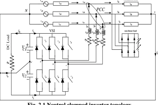
NEUTRAL CLAMPED INVERTER TOPOLOGY
There are various voltage source inverter are presented eminent researchers, but among those the neutral clamped inverter topology has gained considerable attention to load balancing, harmonics reduction and power factor correction. A three phase four wire neutral clamed inverter circuit has shown in Fig. 2.1. It is well published in [12-14]. In this circuit the junction (
n
) of the two capacitors is connected to the neutral of the load and source. A path for zero sequence current flows through this neutral wire. Therefore the three injected currents of voltage source inverter can be independently controlled. In this configuration there is no isolation transformer and each leg of the VSI is connected to the point of common coupling through an interface inductor with small resistance which is equivalent inductor resistance.isa isb isc
non linear load Unbalanced Load PCC
ila ilb ilc ifb
ifc ifa Lfa Lfb Lfc
zla zlb zlc
1 s
3 s
4 s
6 s a
b
2 s 5 s
c
i0 v sa
vsb
v sc zsa zsb zsc
N
Rfa Rfb Rfc
+ +
n'
n
i0
i1
i2
c1
v
c2
v
D
C
L
o
a
d
VSI
Rdc
idc
Fig. 2.1 Neutral clamped inverter topology
The topology consists of six switches and there are no isolation transformers. The problem of saturation due to dc current does not arise due to absence of transformers. This topology employs two dc storage capacitors (C1 and C2) of same rating. The topology provides the independent tracking of the three reference
currents and compensates the zero sequence load current. However it has serious disadvantage that due dc component of load current the voltages of the capacitors do not remain constant shown in [15-16]. Because of the unequal leakage currents, unequal delay in the semiconductor switch, asymmetric charging of the capacitors during transient conditions, the state space model will be developed. This model will be used for ac load compensation, which may be unbalanced and contain harmonics. To equate the unequal capacitor voltage PI controller will be used, explained in the following section.
III.
EXTRACTION OF REFERENCE COMPENSATOR CURRENTS UNDER NON
STIFF AND UNBALANCED SOURCE VOLTAGES
A three phase, four wire compensated system [15] is shown in Fig.1. The three phase load considered is unbalanced and non linear, the three phase supply voltages and currents also considered unbalanced [16-17]. The compensator , linear and non linear loads are connected at a point called the point of common coupling (PCC), accordingly the compensator has to inject currents in to the line equal and opposite to load currents, then the source currents are free harmonics. The compensator is considered is idle and it is comprised of idle three phase voltage source inverter [18-19].
The basic scheme is shown in Fig. 3.1. In this scheme the compensator is represented by current sources. The aim of the scheme is to generate the three reference current waveforms for
i
fa,i
fb andfc
i
, denoted by *ifa,i*fb, and
i
*fc ,respectively, from the measurements of source voltages and load currents such that the supply sees a balanced load. No assumption on the nature of the load is required. The compensator will produce desired results as long as its bandwidth is sufficient to follow the fluctuations in the load. The reference currents are generated using the theory of the instantaneous symmetrical components.Let any three phase instantaneous currents be defined by,i
fb, ifc and . The power invariant instantaneous
n
*
ifa
ifb
*
ifc
*
sa
i
sb
i
sc
i
la
i
lb
i
lc
i
N
sa
v
sb
v
sc
v
Unbalanced Non linear Load
PCC
Unbalanced Non linear Load
Unbalanced Non linear Load
U
n
b
al
an
ce
d
D
is
to
rt
ed
S
o
u
rc
e
V
o
lt
ag
es
Ideal Compensator
Fig.3.1 Line diagram of 3-phase, 4-wire compensated system 3.1 Definition of Instantaneous Symmetrical Components
A three phase four wire compensated system as shown in Fig. 3.1. In the system all the three phases are connected with unbalanced non linear loads, power fed to these loads from the source is also unbalanced and distorted in all the three phases. To compensate this unbalanced non linear loads under defined conditions a shunt active power filter have been connected which is shown as an ideal current source [12-14].
Let the unbalanced and distorted supply voltages can be represented as
(1)
In Eqn. (1) the subscript„s‟ stands for supply, a,b,c stands for three phase notation, m- is maximum or peak value of supply voltage and n- for harmonic number. K-for upper harmonics responsible for voltage distortion,
vsn
stands for phase angle of nth harmonics in voltage.Instantaneous values of the zero sequence
a
0( )
t
, positive sequence
a
1( )
t
and negative sequence
a
2( )
t
components have been extracted using instantaneous symmetrical components theory.0( )
1 1 1 ( )
1
1( ) 1 2 ( )
3 2
2( ) 1 ( )
t
a a t
t a a t
a b
t
a a c
t a
(2)
Where variables
a ,
b and
c denote the instantaneous values of three phase voltages or currents quantities in all the three phases a, b and c respectively. The term „a‟ is a complex operator which is equal to2 3
j
e
. The zero sequence, positive sequence and negative sequence voltages can be calculated as follows.
( )
1 2
012 012( ) 2
1
t T j wt
Vsa vsa t e dt
t
T (3)
012 0 1 2
[ ]
Vsa Vsa Vsa Vsa is a column vector, with samples if zero, positive and negative with respect to voltage phasor. The subscript
stands for transpose operator. Whereas T stands for average value of voltage and current wave a form time period.The voltage phasor are expressed as follows
( ) sin( )
1
( ) sin( )
1
( ) sin( )
1
k
Vsa t Vman nwt vsn
n k
Vsb t Vmbn nwt vsn
n k
Vsc t Vmcn nwt vsn
n
0 0 0
1 1 1
2 2 2
Vsa Vsa Vsa
Vsa Vsa Vsa
Vsa Vsa Vsa
(4)
By considering above equations the fundamental zero sequence, positive sequence and negative sequence voltages have found.
0 0 0
( ) 2 sin( )
0 0 0
( ) 2 sin( )
0 0 0
( ) 2 sin( )
Vsa t Vsa t Vsa
Vsb t Vsa t Vsa
V t Vsa t Vsa
sb
(5)
1 1 1
( ) 2 sin( )
1 1 2 1
( ) 2 sin( )
3
1 1 2 1
( ) 2 sin( )
3
Vsa t Vsa t Vsa
Vsb t Vsa t Vsa
V t Vsa t Vsa
sb
(6)
2 2 2
( ) 2 sin( )
2 2 2 2
( ) 2 sin( )
3
2 2 2 2
( ) 2 sin( )
3
Vsa t Vsa t Vsa
Vsb t Vsa t Vsa
V t Vsa t Vsa
sb
(7)
From Eqn. (5)-( 7) its showing that calculation of zero sequence, positive sequence and negative sequence voltages only one phase synchronization is enough (say phase-a).
The objective of three phase four wire system here it is to provide balanced sinusoidal supply currents under unbalanced and distorted supply voltages these supply currents are after compensation assumed as
i
sac,
i
sbc andc sc
i
(here c-stands for compensated source currents) then the zero sequence current carried by the neutral wire is zero.0
c c c
isa i isc
sb
(8)
Net task is to control over power factor angle
(
1)
which angle between positive sequence voltage(
v
1sa)
and positive sequence current
(
i
1sa)
.From Eqn. (2) used to find the positive sequence voltage and current which are (
v
1sa,i
1sa) because the angle between them is the power factor angle
1which is equivalent to angle between balanced supply voltages and reference currents. This can be found using instantaneous values of voltages and currents (v
sa,
v
sb,
v
sc) and (,
,
sa sb sc
i
i
i
). This power factor can be set to any desired value in this algorithm.Assume instantaneous current
i
1sa lags that of instantaneous voltagev
1sa by an angle
11 1 1
(vsa( ))t (isa( ))t
(9)
2
c c 2c
1vsa avsb a vsc isa aisb a isc
(10)
Substituting the values of a and
a
2 in the aboveequation
1
1
3
1
1
3
12
2
2
2
2
2
c c c c c
sa sb sc sb sc sa sb sc sb sc
v
v
v
j
v
v
i
i
i
j
i
i
1 1 1
tan K1 K2 tan K3 K4 (11) Where,
3
1 2
K vsb vsc , 2 1 1
2 2
K vsa v vsc
sb
, 3 3
2
c c
K isbisc and
4 2 2
c c
i i
c sb sc
K isa
Taking tangent to both sides of (11) we get.
tan
11 1 1 3 4
tan[tan 3 4 ]
1
2 1 3 4 tan
K K
K
K K
K K K
Substitute K1, K2, K3 and K4 in the above equation.
v
sb
v
sc
3
v
sa
i
sac
v
sc
v
sa
3
v
sb
i
sbc
v
sa
v
sb
3
v
sc
i
scc
0
(12)Where
tan
13
In the above equation (12), if we assume power factor angle is zero, supply of reactive power from the source is zero. Is this angle is non zero the source has to supply reactive power which is
times the instantaneous power.In balanced circuit the instantaneous power is constant, but in unbalanced circuit it has double frequency component in addition to the dc value. Because of this harmonics the instantaneous power will be oscillating. So the objective of the compensator here is to supply oscillating component that is source has to supply average value of the load power.
c c c
vsa sai vsb sbi v isc sc Plavg (13)
The source has to supply real power required by the load, because the load having harmonic component it does not required.
Since the harmonic component is the load does not require any real power, the source only supplies the real power required by the load.
Combining (8) and (13) will get
1
1
1
00 0 0
3 ( ) 3 ( ) 3 ( ) 0
c isa
c vsb vsc vsa vsa vsc vsa vsb vsb vsa vsb vsc vsc isb
c P
i
vsa vsb vsc sc lavg
(14)
1
1
1
00 0 0
3 ( ) 3 ( ) 3 ( ) 0
c isa
c
i v vsc vsa vsa vsc vsa v v vsa v vsc vsc
sb sb sb sb sb
c P
isc vsa vsb vsc lavg
(15)
Where
v
sa0 the zero sequence voltage is will present when the supply voltages are unbalanced, its zero under balanced supply voltages, in this case we have not assumed that the source voltages are balanced and sinusoidal.Apply KCL at PCC in Fig. 3.1 solve for reference filter currents.
* c
isj ilj isj
j abc (16)
Substituting Eqn. (15) in (16) and solve for reference filter currents will get
0
( )
*
( )
0
( )
*
( )
0
( )
* ( )
dc
dc
dc
vsa vsa vsb vsc
ifa ila Plavg p
vsb vsa vsc vsa
ifb ilb Plavg p
vsc vsa vsa vsb
ifc ilc Plavg p
(17)
Where
(
v
sa2
v
sb2
v
sc2) 3(
v
sa0)
2 if the load is balanced and
1is the same as of the phase of the load current, the compensator currents become zeroThe following observations have made from the above algorithm they are as flows
2. User defined power factor is possible with this the source will supply load power at specified displacement power factor according to the Eqn. (12).
3. The source will supply only average load power according to the Eqn. (13)
Irrespective of the weather supply voltage unbalanced or distorted the above conditions meets always but the source currents are unbalanced and distorted under unbalanced distorted supply conditions. To remove this condition or limitations in the above algorithm positive sequence supply voltages are extracted using Eqn. (6) these voltages will be substituted in Eqn. (17) to generate reference compensator currents.
1 1 1
( )
* ( )
1 1 1
( )
*
( )
1 1 1
( )
* ( )
dc
lavg dc
lavg dc
vsa vsb vsc
ifa ila Plavg P
vsb vsc vsa
ifb ilb P P
vsc vsa vsb
ifc ilc P P
(18)
Where
1 2 1 2 1 2
(
)
(
)
(
) )
v
sa
v
sb
v v
sc . Under unbalanced and distorted supply voltages this algorithms gives balanced source currents after compensation.The objective here is to hold the average capacitors voltage i.e.
1 2
vc vc to a constant. That is equal
to2V
c ref , where
V
cref is the reference voltage of each capacitor. We have1 1 1
1
vc i dt
C
and 1 2
2 2
vc i dt
C
,
(currents i1 and i2 are shown in Fig. 4.1,
v
c
v
c1
v
c2 gives a good indication of the deviation of the average voltage value of the capacitor current from zero. We thus choose a simple proportional plus integral (PI) controller of the formdc p c i c
P k e k
e dt (19)
2
1 2 1 2
ec ec ec vcref vc vc (20)
Where
,
1 1 2 2
e v v e v v
c cref c c cref c (21)
The above algorithm gives balanced source currents after compensation irrespective of unbalanced and distorted supply voltages with non stiff source condition.
IV.
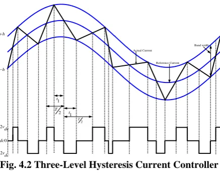
PWM HYSTERESIS CURRENT CONTROLLER
The linear current controller generates required variable voltage which is then fed into single or multiple pulsed width modulation (PWM) to generate the gate drives switching pulses for voltage source inverter (VSI). The non linear current controller‟s works on pre defined hysteresis band, in which the actual currents are compared with the reference compensator currents which are generated based on instantaneous symmetrical components theory under unbalanced and distorted source voltages, discussed in previous section. 4.1 Two-Level Hysteresis Current Controller
Actual Current Reference Current
Band width
2vdc
2vdc
h
h
1
t T
In conventional hysteresis current controller, the inverter output current is made to follow the reference current generated by the algorithm strictly with certain hysteresis band. Hysteresis current controller operates PWM voltage source inverter by comparing reference current with actual filter current in a pre defined hysteresis bands (upper and lower) shown in Fig. 4.1. The current error is difference between the desired (reference) current and the actual current generated by the inverter. The basic logic is as given below.
If the actual current in certain leg is greater than reference current plus hysteresis band (h/2) then it has to be decreased so the bottom switch has to be turned ON and top switch of the same leg has to be turned OFF at the same time. If the actual current is less than reference current minus hysteresis band (h/2) then it has to be increased so the bottom switch has to be turned OFF and top switch of same leg has to be turned ON at the same time. In this two level switching strategies does not use the inverter zero condition, it uses 2Vdc and
2Vdc
only.
The variation of the switching frequency depends on the value of interface inductance, this variation of switching frequency influence the performance of current controlled VSI in terms of maximum switching frequency and harmonics.
4.2 Three-Level Hysteresis Current Controller [2]
The implementations of a three level hysteresis current controller are set as upper and lower band. The reference current for this three level hysteresis controller are derived from positive sequence of supply voltage based on instantaneous symmetrical component theory discussed in the above section. When the actual current reaches to an outer hysteresis band, at that particular instant of time the inverter output is set to an active positive or negative output to force the reversal of actual current. Accordingly the actual current reaches to an inner hysteresis boundary (this inner hysteresis boundary is nothing but the reference current generated from theory of positive sequence extraction of instantaneous symmetrical component), at this time the inverter output is set to a zero condition and the actual current will be forced to reverse direction without reaching the next outer boundary. If the selection of a zero inverter output does not reverse the actual current, it will continue though the inner boundary to the next outer hysteresis boundary, at that time an opposite inverter output will be commanded and the current will reverse.
The switching process of three level hysteresis current controller as shown in Fig.4.2. The MATLAB program for phase-a switching is as follows.
if ierra>0 if ierra>=(h) swa=1; end
elseif ierra<=del swa=0;
end
if ierra<0 if ierra<=(-h) swa=2; end
elseif ierra>=(-del) swa=0;
end
If swa=1implies that the switch state is 2Vdc
elseif swa=0 implies the switch state is zero elseif swa=2 implies the switch state is 2Vdc
Actual Current
Reference Current Band width
2vdc
2v dc
h
h
1
t
0
v dc
2
T
1
t
2
T
Fig. 4.2 Three-Level Hysteresis Current Controller 4.3 State Space Model for VSI
The gating signal for switch S1in Fig. 2.1 is represented by a binary variableSa. IfSa 1, S1is
closed, and ifSa 0, S1is open. A gating signal for
4
S is the complementary signal that is ifSa 0,
4
S is
open, and if Sa 1, S4 is close. SimilarlyS
b,Sb, Sc , Sc , and represent gating signals for switches S3 ,
6
S , S5 and S2 respectively. The switches of the inverter will be operated by generating switching signals to most positive group and most negative group in complementary form such that in each leg one of the switches is always gated. Accordingly by operating the switches the input currents to the inverter i1 and i2 are derived
from Fig. 3.3.
1
i Saifa S ib fb S ic fc (4.1)
2
i Saifa S ib fb S ic fc (4.2)
The voltage source inverter configuration of switches S1 to S6 is operated in the three level hysteresis
current control mode. When the filter current i fa touches the pre-calculated lower limit of hysteresis band, switch S1 is closed. When the filter curent reaches to the inner band which is reference current generated usig
contol theory, the swithcS1is opens and zero state will be applied. If the selection of a zero inverter output does not reverse the actual current, it will continue though the inner boundary to the next outer hysteresis boundary whichS4, will closes, at that time an opposite inverter output will be commanded and the current will reverse. The equivalent circuit for this mode is shown in Fig 4.3.
2
closed S1
opened S4
f
R Lf
_ + vsa
fa
i
+
-1
c
v
+
-c
v 2
C
1
C
'
n
N
1
i
2
i
RS LS
Unbalanced Non Linear
Loads
Source impedance Filter Resistance &
Inductance
1
v
difa Rf RS c v
sa
ifa
dt L LS L LS L LS
f f f
(4.3)
Similarly if the current hits a pre-calculated upper limit, switch is opened and is closed. From an equivalent circuit similar to Fig. 4.2, we can write,
2
c
fa f S sa
fa
f S f S f S
v
di
R
R
v
i
dt
L
L
L
L
L
L
(4.4)From equation (4.3) and (4.4) combined to get the following equation.
1 2
v v
difa Rf RS c c v
sa
ifa Sa Sa
dt L LS L LS L LS L LS
f f f f
(4.5)
Similarly for phase‟s b and c, we have,
1 2
c c
fb f S sb
fb b b
f S f S f S f S
v
v
di
R
R
v
i
S
S
dt
L
L
L
L
L
L
L
L
(4.6)1 2
c c
fc f S sc
fc c c
f S f S f S f S
v
v
di
R
R
v
i
S
S
dt
L
L
L
L
L
L
L
L
(4.7)In Fig. 4.3 the switch can be closed and opened or vice versa. In each case KCL can be applied at nodes 1 and 2, and KVL can be applied around the loop of the closed switch. The resulting equations can be combined with the help of (4.1) and (4.2) and binary variables and to obtain the following, assuming
1
c fa fb fc
a b c
dv i i i
S S S
dt C C C
2 fa fb fc C
a b c
i i i
dv
S S S
dt C C C (4.8)
0 0
dvdc
dt (4.9)
We obtain the following state space model
x Ax Bu (4.10)
Where 1 11 12 1 1
2 21 22 2 2
x A A x B
d
u
x A A x B
dt
,
1
x
i
i
i
fa
fb
fc
,x
2
v
c1v
c2v
dc0
[
]
t
u
v
sa
v
v
sc
sb
0 0 0 0 11 0 0R RS f L L
S f
R RS f A
L L S f
R RS f L L S f 0 0 12 0
Sa S a
Lf LS Lf LS
Sb S b
A
Lf LS Lf LS
Sc S c
Lf LS Lf LS
, 21
0 0 0
S
Sa b Sc
C C C
Sa Sb Sc A
C C C
, 1 0 0 1 0 0 1 1 0 0 L f B L f L f
0 0 0
0 0 0
22
0 0 0
A ,
0 0 0 0 0 0 2
0 0 0
B
V.
SIMULATION RESULTS AND ANALYSIS
To understand the actual compensator, a neutral clamped 3-phase, 4-wire voltage source inverter is chosen and simulated in MAT Lab environment [14], shown in Fig.2.1. The load and the compensator are connected at the point of common coupling (PCC). The voltage source inverter is consisting of six IGBT switches each with anti parallel diodes which allow the flow of current in both the directions. The middle point of the two capacitors is connected to the neutral of the load. The midpoint of the inverter legs are connected to the PCC through interface inductor. A small resistance is considered which interface inductor resistance.
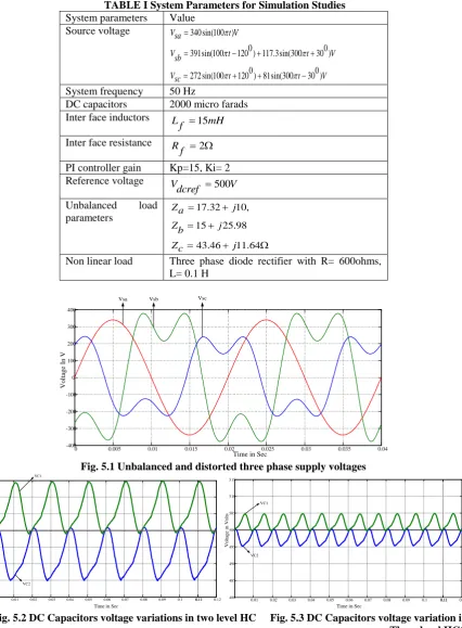
The system parameters for the simulation studies are given in Table 1.
TABLE I System Parameters for Simulation Studies System parameters Value
Source voltage 340 sin(100 )
0 0
391sin(100 120 ) 117.3sin(300 30 )
0 0
272 sin(100 120 ) 81sin(300 30 )
Vsa t V
Vsb t t V
Vsc t t V
System frequency 50 Hz
DC capacitors 2000 micro farads Inter face inductors L 15mH
f
Inter face resistance R 2
f
PI controller gain Kp=15, Ki= 2 Reference voltage V 500V
dcref
Unbalanced load parameters
17.32 10, 15 25.98 43.46 11.64
Za j
Z j
b
Zc j
Non linear load Three phase diode rectifier with R= 600ohms, L= 0.1 H
0 0.005 0.01 0.015 0.02 0.025 0.03 0.035 0.04
-400 -300 -200 -100 0 100 200 300 400
Vsa Vsb Vsc
V
o
lt
ag
e
In
V
Time in Sec
Fig. 5.1 Unbalanced and distorted three phase supply voltages
0.11 0.11 0.09 0.07
0.05 0.03
0.01 0.02 0.04 0.06 0.08 0.1 0.12 480
485 490 495 500 505 510 515
VC1
VC2
V
o
lt
ag
e
in
V
o
lt
s
Time in Sec
0.11 0.11 0.09
0.07 0.05
0.03
0.01 0.02 0.04 0.06 0.08 0.1 0.12 480
485 490 495 500 505 510 515
Time in Sec
V
o
lt
ag
e
in
V
o
lt
s
VC2 VC1
In section 4 explained state space model of three level hysteresis current controllers. According to the Fig. 4.1 and 4.2, in the three levels HCC the compensator can use positive, negative and zero level of the inverter output. Due to this zero level switching, the variation of voltage across two capacitors is reduces which is shown in Fig. 5.3. The voltage variation across two capacitors in two level shown in Fig. 5.2. In this it is clearly shown that, under two level HCC voltage variations is more, whereas in three level voltages variation reduces considerably.
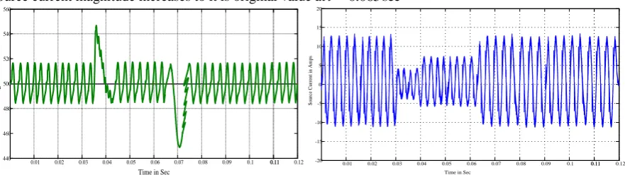
4.4 Transient performance of DC link Voltage controller in two levels HCC
The Eqn. (19) is used to generate DC load power including losses in the inverter. While maintaining this dc load power constant using PI controller under two level HCC, it is possible to maintain the capacitor voltage also constant. From the Fig. 5.4 it is observed that, initially the compensator is operated under steady state conditions. Att 0.03sec, load is suddenly reduced to half of it is original. Due to this sudden reduction
of load, power consumed by the load reduces and the capacitor absorbs surplus power supplied by the source. Because of this surplus power the capacitor voltages will increase above the reference value. Using PI controller gain the variation in the capacitor voltages will come back to it is reference value att 0.045sec. After few cycles att0.065sec, the load switches back to it is full load. At this point of time, load requires high amount
of power and this power will be supplied from the capacitors due to which the capacitor voltage will fall down. Again the PI controller action starts and brings the voltage variation in the capacitor to it is reference value within few cycles. From Fig. 5.5, it is observed that the source current changes with respect to the load and dc link voltage changes. Att 0.03sec, the source current magnitude reduces due to reduction of load and the
source current magnitude increases to it is original value att0.065sec
0.11 0.11 0.09
0.07 0.05
0.03
0.01 0.02 0.04 0.06 0.08 0.1 0.12
440 460 480 500 520 540 560
V
o
lt
a
g
e
i
n
V
o
lt
s
Time in Sec Time in Sec
0.11 0.11 0.09
0.07 0.05
0.03
0.01 0.02 0.04 0.06 0.08 0.1 0.12 -20
-15 -10 -5 0 5 10 15 20
S
o
u
rc
e
C
u
rr
en
t
in
A
m
p
s
Fig. 5.4 DC link voltage variation in two level HCC , Fig. 5.5 Source current after compensation in two levels HCC under transient condition. 5.2 Transient performance of DC link Voltage controller in three levels HCC
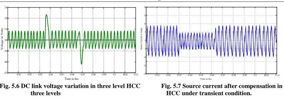
The Eqn. (19) is used to generate DC load power including losses in the inverter. While maintaining this dc load power constant using PI controller under three level HCC, it is possible to maintain the capacitor voltage also constant. From the Fig. 5.6 it is observed that, initially the compensator is operated under steady state conditions. Att0.03sec, load is suddenly reduced to half of it is original. Due to sudden reduction of
0.11 0.11 0.09
0.07 0.05 0.03
0.01 0.02 0.04 0.06 0.08 0.1 0.12
470 480 490 500 510 520 530
V
o
lt
a
g
e
i
n
V
o
lt
s
Time in Sec Time in Sec
0.11 0.11 0.09
0.07 0.05
0.03
0.01 0.02 0.04 0.06 0.08 0.1 0.12 -20
-15 -10 -5 0 5 10 15 20
S
o
u
rc
e
C
u
rr
en
t
in
A
m
p
s
Fig. 5.6 DC link voltage variation in three level HCC Fig. 5.7 Source current after compensation in
three levels HCC under transient condition.
VII.
CONCLUSION
This paper presents a state space model for three phase four wire systems with non stiff source. A control algorithm has proposed to compensate AC and DC components under unbalanced non linear loads. Initially a fixed unbalanced load will be considered in three phases along with non linear load. It is observed that after compensation the source currents are balanced and in phase with source voltage. The source currents observed balanced even after increasing the load in all three phases. A two level and three level hysteresis current controller has been used to generate switching commands for inverter switches.
BIOGRAPHIES
K.Srinivas received the B.E. degree in electrical and electronics engineering from Chithanya Bharathi Institutue of Technology and Science, Hyderabad, Osmania University, Hyderabad, India, in 2002, the M.Tech. Degree in power systems and Power Electronics from the Indian Institute of Technology, Madras, Chennai, in 2005, pursuing Ph.D from Jawaharlal Nehru Technological University Hyderabad. Currently, he is an Assistant Professor in Electrical and Electronics Engineering Department, Jawaharlal Nehru Technological University Hyderabad College of Engineering Karimanagar. His fields of interest include power quality and power-electronics control in power systems.
S.S.Tulasi Ram received the B.Tech, M Tech and Ph.D Degrees in electrical and electronics engineering from Jawaharlal Nehru Technological University Hyderabad India, in 1979, 1981 and 1991rescpectively. Currently, he is a Professor in Electrical and Electronics Engineering Department, Jawaharlal Nehru Technological University Hyderabad College of Engineering Kukatpally, Hyderabad. His fields of interest include HVDC Transmission systems, Power system dynamics, Power Quality in power electronics, Smart energy management.
REFERENCES
[1]. M. Bollen, Understanding Power Quality Problems: Voltage Sags andInterruptions. New York: IEEE Press, 1999.
[2]. Karuppanan P, Saswat Kumar Ram and KamalaKanta mahapatra “Three level Hysteresis current controller based Active power filter for harmonic compensation, Proceedings of ICETECT 2011, pp 407-412.
[3]. B. Singh, K. Al-Hadded and A. Chandra, “A review of active filters for power quality improvements,” IEEE Trans. Industrial Electronics, Vol. 46, No. 5, Oct. 1998, pp. 960-971.
[4]. Arindam Ghosh, SMIEEE and Avinash Joshi, “A new approach to load balancing and power factor correction in power distribution system”. IEEE Transactions on power Delivery, 2000, pp 417-422. [5]. K.srinivas, Dr S S Tulasi Ram” A Control Algorithm of Power Factor Correction for single phase shunt
active power filter under distorted supply voltages/currents” IJAREIE, Vol. 3, Issue 2, February 2014. [6]. K.srinivas, Dr S S Tulasi Ram” A Three Phase Four Wire Shunt Active Power Filter Control
Algorithm” IJACR, Vol. 4, Issue 14, March 2014. [7]. under Unbalanced and Distorted Supply Voltage
[9]. Andrea Cavallini and Gian Carlo Montanari, “Compensation Strategies for Shunt Active-Filter Control.” IEEE Trans, On Power Electronics, Vol. 9, NO. 6, November 1994.
[10]. Fag Zheng Peng, and Jih-Sheng Lai, “Generalized Instantaneous Reactive Power Theory for Three-Phase Power Systems.” IEEE Trans, On Instrumentation and Measurement, Vol. 45, No. 1, February 1996.
[11]. Linash P. K. and Mahesh K. M., A control algorithm for single-phase active power filter under non-stiff voltage source, IEEE Trans. on Power Electronics, May 2006, Vol. 21, No. 3. pp. 822-825. [12]. H. Akagi and R. Kondo, “A transformer less hybrid active filter using a three-level pulse width
modulation (PWM) converter for a medium- voltage motor drive,” IEEE Trans. Power Electron., vol. 25, no. 6, pp. 1365–1374, Jun. 2010.
[13]. A. Nabae, S. Ogasawara and H. Akagi, “A novel control scheme for current-controlled PWM inverters,” IEEE Trans. on Industrial Application, Vol. IA-22, No. 4, Julu/Aug. 1986, pp. 697-701 [14]. Mahesh, K. M. and K. Karthikeyan (2006) A study on design and dynamics of voltage source inverter
in current control mode to compensate unbalance and non-linear loads. Proceedings of IEEE International Conference on Power Electronics, Drives and Energy Systems for Industrial Growth, New Delhi, December, 1-8.
[15]. U. K. Rao, M. K. Mishra, and A. Ghosh, “Control strategies for load compensation using instantaneous symmetrical component theory under different supply voltages,” IEEE Trans. Power Del., vol. 23, no. 4, pp. 2310–2317, Oct. 2008.
[16]. A. Sahoo and T. Thyagarajan, “Modeling of facts and custom powerdevices in distribution network to improve power quality,” in Proc. Int. Conf. Power Syst., 2009, pp. 1–7.
[17]. Arya, S.R. ; Singh, B.Generation, Transmission & Distribution, IET , Implementation of distribution static compensator for power quality enhancement using learning vector quantisation, Generation, Transmission & Distribution, IET , Jan 2014, Vol. 7, No. 11. pp. 1244- 1252.
[18]. Thanh Hai Nguyen ; Dong-Choon Lee ; Chan-Ki Kim , A Series-Connected Topology of a Diode Rectifier and a Voltage-Source Converter for an HVDC Transmission System, IEEE Trans. on Power Electronics, Jan 2014, Vol. 29, No. 4. pp. 1579- 1584.