Asian Journal of Applied Science and Technology (AJAST) (Open Access Quarterly International Journal) Volume 2, Issue 2, Pages 329-336, 2018
Performance Analysis of Low Power and High Speed CRC Generator Using group
of D flip-flops based on 12T Memory Cell
M.Ananthi1, P.Bharathi2 and P.Manimekalai3
1,2Assistant Professor, Department of Electronics and Communication Engineering, Ariyalur Engineering College, Tamil Nadu, India. 3UG Student, Department of Electronics and Communication Engineering, Ariyalur Engineering College, Tamil Nadu, India.
Article Received: 27 January 2018 Article Accepted: 23 February 2018 Article Published: 15 April 2018
1.INTRODUCTION
MEMORIES are extensively used in aerospace applications as the medium to store data in which single event
upsets (SEUs) induced by radiation particles are becoming one of the most significant issues. Because they can
conduce to the data corruption in a memory chip and the circuit itself is not permanently damaged, SEUs are also
described as the soft errors. Therefore, SEUs can cause a malfunctioning of an electronic system. In some critical
memory applications (e.g., satellite equipment and cardioverter defibrillators, SEUs can be detrimental and crucial.
However, radiation hardening techniques for memories are one of the bottlenecks in providing fault tolerance. For
many years, some radiation-hardening-by-design (RHBD) techniques have been used to tolerate soft errors in
memories using standard commercial CMOS foundry processes, with no modifications to the existing process or
violation of design rules.
SRAM-based field-programmable gate arrays (FPGAs) have been widely used during the last decades. However,
the volatility of SRAM has limited FPGAs in applications where high security and instant power-on are required.
The problem can be solved by introducing non-volatile memory (NVM) as the configuration bit. However, the
traditional NVM devices, such as anti-fuse, E2PROM, and flash, require high-voltage process and have poor logic
compatibility, thus limiting the logic density and increasing the integration cost of FPGAs.
The remainder of this paper is mainly divided into the following sections. Section II introduces the proposed RHBD
12T cell structure and analysis. In Section III, simulations, and the detailed analysis of improved version is shown.
2.NOVEL RADIATION-HARDENED-BY-DESIGN (RHBD) 12T MEMORY CELL
The proposed RHBD 12T memory cell is shown in Fig. 1. Here, two access transistors, pMOS transistors P5 and
P6, have been connected bit-lines BLN and BL to the output nodes QN and Q, respectively. A B S T R A C T
The proposed implementation of a novel radiation-hardened-by-design (RHBD) high speed CRC Generator architecture using gate diffusion input technique. The main objective of CRC generator is used for error detection in communication systems. The Gate Diffusion Input logic is a technique that is used to reduce transistor count and power consumption of sequential circuits. The hardware component of CRC is consists of group of D flip-flops. Here the gate diffusion input logic based D flip-flop is a basic cell to design a CRC Generator, maintaining low complexity of logic design. The proposed architecture is validated by Tanner EDA tool and implementation on Spartan 6 FPGA development board series.
Fig.1. Proposed RHBD 12T memory cell
Considering the stored 1 state (i.e., QN = 0, Q = 1,S0 = 0, and S1 = 1) for the proposed RHBD 12T cell. When
word-line WL is high state 1, transistors P1, P4,P7, N2, and N3 are ON, and the remaining transistors are OFF.
Before read operation is executed in the proposed 12T memory cell, two bit-lines BL and BLN need to be recharged
to supply voltage VDD. After read operation, and word-line WL is 0 state, the output node Q will store its original
state 1 without changing. Fig. 2 shows a “write 0, read 0, write 1, and read 1” transient simulation result. From Fig.
2, we can see that the proposed cell can rightly achieve write and read operations.
Fig.2. Transient simulation result of the proposed RHBD 12T cell
3.PERFORMANCE ANALYSIS OF LOW POWER AND HIGH SPEED CRC GENERATOR USING
GROUP OF D FLIP-FLOPS
The basic GDI cell was used to design of combinational circuits and sequential circuit with less number of
transistors and higher energy consumption as compare to conventional CMOS technique. A cyclic redundancy
code can be calculated using one byte oriented method. Configurable CRC generator was implemented for error
detection in communication using various software algorithms. The parallel CRC generator was completed
designed using software approaches for increase the speed in transmission. The parallel and serial CRC generator
unit was designed and functionality was verified by using Verilog language in Xilinx software. The CRC generator
Asian Journal of Applied Science and Technology (AJAST) (Open Access Quarterly International Journal) Volume 2, Issue 2, Pages 329-336, 2018
linear feedback register was analysed with the help of simulation software. The parallel CRC generator addresses
the issues of number of look up tables and critical path delays of various checkers in the polynomial expression.
The folding, pipelining and retiming are the methods used for reducing the delay of the circuits without changing
the functionality of the circuit and also maintaining the same throughput and date rate for digital communication.
The three techniques are incorporated in parallel CRC generator for improving the throughput. The fast CRC
address the issues of packet size and speed of transmission of bits. The mapping of a tri-level network into linear
pipeline architecture for improving the throughput with the help of place and route approach of FPGA design. The
each message bit rate was designed into number of execution units for reducing the latency. The hardware
implementation for computing matrix in checksum was proposed and the data to be process in parallel manner. The
parallel CRC generator process all the bits parallel with minimum number of cycles for less propagation delay and
analysed in Verilog language using Xilinx software. This paper presents the implementation of CRC generator
using area and power efficient gate Diffusion-Input (GDI) D flip flop. The basic configuration of GDI cell is shown
in Figure 3.
Fig. 3. GDI D Flip Flop with Buffer
3.1. Types of errors caused by Radiation
Based on the particle strike the errors can be classified into hard error and soft errors the types of error depend on
whether it is permanent damage or temporary damage. Single event upsets come under the clause of temporary
damage or soft errors. The affected circuits can be recovered by using reset signals or by correction circuits. Hard
errors are due to permanent damages. These errors cannot be corrected or the circuits cannot be recovered by
correction mechanisms Single Event Burnout (SEB) , Single Event gate rupture ( SEGR) and single event latch
up ( SEL) comes under this category. In this review we are going to review about the Single Event Upset which is
soft error and which occurs in memories. These SEUs cause transient errors in combinational circuits and makes bit
flips in sequential circuits. The CMOS SRAM basic cell is considered. An extensive study had been done with the
detection and correction schemes for 6T SRAM cell. The similar simulations for CNTFET SRAM was done and
4.SIMULATION AND IMPLEMENTATION
Detailed SPICE simulations were carried out on the proposed RHBD latch using advanced Predictive Technology
Model (PTM) invented by the nano- scale Integration and Modeling (NIMO) Group of Arizona State University.
As an evolution of raditional Berkeley Predictive Technology Model (BPTM), PTM of bulk CMOS is successfully
generated for 130 to 32 nm technology nodes. The PTM can be easily customized to cover a wide range of process
uncertainties. PTM is more physical, scalable, and continuous over technology generations and suitable for
emerging variability and reliability issues. The 45 nm technology model card was chosen to perform the
simulations. The proposed work was implemented in Xilinx using VHDL. Considering the stored 1 state (i.e., QN
= 0, Q = 1, S0 = 0, and S1 = 1) for the proposed RHBD 12T cell. To write data 0 into the proposed 12T cell,
word-lineWL and bitline BL need to be 0 state, and bitline BLN must be 1 state. Subsequently, node Q will be
pulled down to 0 state, and node QN will be pulled up to 1 state.
4.1.SEU injection simulation
As mentioned in section 3, all the internal nodes were partitioned into different equivalent class of nodes so that
SEU injection was only performed on three internal nodes from each equivalent class of nodes: {N1, N2} , {N4, N7
} , { N3, N5, N6, N8, N9, N10} . SEU injection methodology is to simulate the high-energy particle striking. The
current induced by SEU can be modeled as traditional double-exponential function cur- rent source, which can
accurately represent the electrical impact of particle striking. The pulse can be expressed as
Asian Journal of Applied Science and Technology (AJAST) (Open Access Quarterly International Journal) Volume 2, Issue 2, Pages 329-336, 2018
4.2. Delay and power comparison
The structure of the reference latch and TMR-latch. A performance comparison between the proposed latch, the
reference latch and TMR-latch (note that the result is normalized by the reference latch). the propagation delay of
the proposed latch is 83% of the TMR-latch, and the power dissipation of the proposed latch is 68% of the
TMR-latch. In short, the simulation results reveal that the proposed latch is delay and power efficient in comparison
with TMR-latch.
4.3. DICE Cell
As shown I n Fig.1, the DICE cell uses twice the number of transistors of a standard storage cell. The DICE cell
has two states, the 0 state (X1=0, X2=1 , X3=0, X4=1) and the 1 state (X1=1, X2=0, X3=1, X4=0). In any of these
two states upon the occurrence of a soft error (on a single node), the state of the node is always driven back to its
original value. For example, in the 0 state, if the node struck by a particle is X2, the state of X2 goes from 1 to 0.
However, this strike will not propagate along the feedback loop due to the interlocked configuration. Meanwhile,
the state 0 stored in X1 can restore the state of X2; however, when a single event (strike) occurs on multiple nodes,
the DICE cell is unable to drive back the original state. For example, in the 0 state, if the node struck by a particle
is X2, the state of X2 goes from 1 to 0. Meanwhile, if node X1 is also affected by the strike, then it goes from 0 to 1.
In this case, due to the strike on X1, the state of X2 will not be restored and a soft error is said to occur. Simulation
results show that if there is a strike on X1, a very small amount of charge on X2 can change the state of the DICE
cell.
Fig: DICE proposed cell
4.4. 12T Hardened Cell
A single node hardened memory cell has been proposed in. The basic storage element used in this memory cell
relies on the hardening scheme of. In the memory cell its feedback loop is cut off by the transistors M5, M6, M7,
and M8, i.e. for a single node upset, a transient pulse cannot be propagated along this loop back to its starting point.
The gates of the PMOS and NMOS transistors are separated from the hardened nodes a1 and a2. Signal
regeneration at a1 and a2 is controlled by the transistors M5 and M8. In this cell, the access pass gates (M1 and M2)
are connected to node d instead of nodes a1 and a2 to prevent the high leakage current from BL to change the data
stored in the memory cell. A TF on a1 or a2 will not change the data stored in the memory cell. A NMOS write
opera tes correctly when writing a “0” as data, but it may encounter problems when writing a “1”. Therefore, a write control transistor is added between M11 and ground to write a “1”. With this write control transistor, the
hardened memory cell consists of eleven transistors, i.e. one transistor less than the DICE cell configuration. The
11T memory cell is unable to restore the state of the node when a single event causes a multiple node upset.
Similar to the DICE cell, the 12T cell has two states, the 0 state (d=0, db=1, a1=1, a2=1) and the 1 state (d=1,
db=0, a1=0, a2=0). If nodes a2 and d are affected by a strike, the state of the 11T memory cell will be changed, i.e.
it has limited tolerance under a single event with a two node upset.
5.CONCLUSION
The proposed implementation of a novel radiation-hardened-by-design (RHBD) high speed CRC Generator
architecture using gate diffusion input technique. The main objective of CRC generator is used for error detection
in communication systems. The Gate Diffusion Input logic is a technique that is used to reduce transistor count and
power consumption of sequential circuits. The hardware component of CRC is consists of group of D flip-flops.
Here the gate diffusion input logic based D flip-flop is a basic cell to design a CRC Generator, maintaining low
complexity of logic design. The proposed architecture is validated by Tanner EDA tool and implementation on
Spartan 6 FPGA development board series.
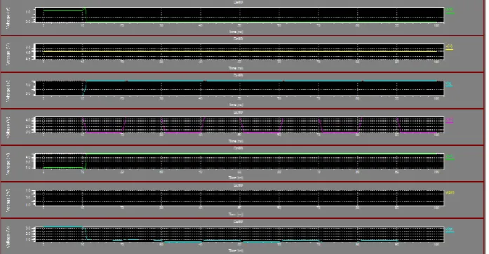
Performance comparison
REFERENCES
[1] E. Ibe, H. Taniguchi, Y. Yahagi, K.-I. Shimbo, and T. Toba, “Impact of scaling on neutron-induced soft
error in SRAMs from a 250 nm to a 22 nm design rule,” IEEE Trans. Electron Devices, vol. 57, no. 7, pp.
Asian Journal of Applied Science and Technology (AJAST) (Open Access Quarterly International Journal) Volume 2, Issue 2, Pages 329-336, 2018
[2] P. E. Dodd and L. W. Massengill, “Basic mechanisms and modeling of single-event upset in digital
microelectronics,” IEEE Trans. Nucl. Sci., vol. 50, no. 3, pp. 583–602, Jun. 2003.
[3] Muthukumaran. N and Ravi. R, 'Hardware Implementation of Architecture Techniques for Fast Efficient
loss less Image Compression System', Wireless Personal Communications, Volume. 90, No. 3, pp.
1291-1315, October 2016, SPRINGER.
[4] Muthukumaran. N and Ravi. R, 'The Performance Analysis of Fast Efficient Lossless Satellite Image
Compression and Decompression for Wavelet Based Algorithm', Wireless Personal Communications,
Volume. 81, No. 2, pp. 839-859, March 2015, SPRINGER.
[5] Muthukumaran. N and Ravi. R, 'VLSI Implementations of Compressive Image Acquisition using Block
Based Compression Algorithm', The International Arab Journal of Information Technology, vol. 12, no. 4,
pp. 333-339, July 2015.
[6] Muthukumaran. N and Ravi. R, 'Simulation Based VLSI Implementation of Fast Efficient Lossless Image
Compression System using Simplified Adjusted Binary Code & Golumb Rice Code', World Academy of
Science, Engineering and Technology, Volume. 8, No. 9, pp.1603-1606, 2014.
[7] Ruban Kingston. M,Muthukumaran. and N, Ravi. R, 'A Novel Scheme of CMOS VCO Design with reduce
number of Transistors using 180nm CAD Tool', International Journal of Applied Engineering Research,
Volume. 10, No. 14, pp. 11934-11938, 2015.
[8] Muthukumaran. N and Ravi. R, 'Design and analysis of VLSI based FELICS Algorithm for lossless Image
Compression', International Journal of Advanced Research in Technology, Vol. 2, No. 3, pp. 115-119,
March 2012.
[9] R. C. Baumann, “Soft errors in advanced semiconductor devices part I: The three radiation sources,” IEEE
Trans. Device Mater. Rel., vol. 1, no. 1, pp. 17–22, Mar. 2001.
[10] H. L. Hughes and J. M. Benedetto, “Radiation effects and hardening of MOS technology: Devices and
circuits,” IEEE Trans. Nucl. Sci., vol. 50, no. 3, pp. 500–521, Jun. 2003.
[11] D. R. Blum and J. G. Delgado-Frias, “Schemes for eliminating transient- width clock overhead from
SET-tolerant memory-based systems,” IEEE Trans. Nucl. Sci., vol. 53, no. 3, pp. 1564–1573, Jun. 2006.
[12] Manoj Kumar. B and Muthukumaran. N, 'Design of Low power high Speed CASCADED Double Tail
Comparator', International Journal of Advanced Research in Biology Engineering Science and
Technology, Vol. 2, No. 4, pp.18-22, June 2016.
[13] N. Muthukumaran, 'Analyzing Throughput of MANET with Reduced Packet Loss', Wireless Personal
Communications, Vol. 97, No. 1, pp. 565-578, November 2017, SPRINGER.
[14] P.Venkateswari, E.Jebitha Steffy, Dr. N. Muthukumaran, 'License Plate cognizance by Ocular Character
Perception', International Research Journal of Engineering and Technology, Vol. 5, No. 2, pp. 536-542,
February 2018.
[15] N. Muthukumaran, Mrs R.Sonya, Dr.Rajashekhara and Chitra V, 'Computation of Optimum ATC Using
Generator Participation Factor in Deregulated System', International Journal of Advanced Research Trends
[16] Keziah. J, Muthukumaran. N, 'Design of K Band Transmitting Antenna for Harbor Surveillance Radar
Application', International Journal on Applications in Electrical and Electronics Engineering, Vol. 2, No. 5,
pp. 16-20, May 2016.
[17] Akhil. M.S and Muthukumaran. N, 'Design of Optimizing Adders for Low Power Digital Signal
Processing', International Journal of Engineering Research and Applications, Vol. 5, pp. 59-65, March
2014.
[18] Muthukumaran. N and Ravi. R, 'Quad Tree Decomposition based Analysis of Compressed Image Data
Communication for Lossy and Lossless using WSN', World Academy of Science, Engineering and
Technology, Volume. 8, No. 9, pp. 1543-1549, 2014.
[19] Marvin Mark. M and Muthukumaran. N, 'High Throughput in MANET using relay algorithm and
rebroadcast probability', International Journal of Engineering Research and Applications, Vol. 5, pp.
66-71, March 2014.
[20] R. Naseer and J. Draper, “Parallel double error correcting code design to mitigate multi-bit upsets in