IJEDR1702304
International Journal of Engineering Development and Research (www.ijedr.org)1955
Abstract - The most fundamental operation of any processor is the addition. For any circuit there are two important parameters that comes into count is high speed and low power consumption. Hence the speed of various modules should be maximized to dominate overall performance. Depending upon these parameters various adders can be invented like Carry Look Ahead Adder(CLA),Carry Skip Adder(CSA) and Ripple Carry Adder (RCA). The main objective of this paper to provide solution of these parameters at very large scale integration such as 8 bit adder. The main objective of this paper is to provide new low power solution for Very Large Scale Integration (VLSI). One of the most effective technique is MTCMOS which utilizes high as well as low threshold voltage transistors. MTCMOS technique has very small power dissipation as compared to conventional technique and simulation is done using cadence virtuoso 180nm CMOS technology. This paper compares 8 bit 16T full adder using MTCMOS with the conventional full adder. MTCMOS circuit has very small power dissipation and high speed. Static power dissipation reduced to large extend.Keywords- RCA, 16T full adder, MTCMOS technique.
________________________________________________________________________________________________________ I. INTRODUCTION
With the increasing demand of high speed arithmetic unit in circuit like processors, DSP chips and image processing units leads to development of high speed adders. Addition is an obligatory and indispensable function in these units. Operations in these devices should have low power, smaller area and operates at higher speed, with the different arrangement in components , power consumption area and delay various adders has been designed such as Conditional Sum Adder, Ripple carry adder, Carry look ahead adder in literature.
CMOS circuit is the building block of most of the digital circuits. Earlier the major concern was area, as the continuously decrease in technology, power supply, operation frequency and increased chip density the main issue is to reduce the power consumption in VLSI design. Power dissipation causes overheating, reduces battery life, in other words it degrades the concept of portability. Therefore reduction in power dissipation is important for integrity, readability, and feasibility of a circuit and to make circuit cost effective. Power dissipation can be reduced by reduction in power supply which ultimately leads to low threshold voltage transistors. Lower threshold voltage of a circuit means higher speed.
Initially size was started to reduce from half micron technology, now it has reached to nm technology. It effectively reduces the speed the power supply of circuit. So it’s very important to put constraint on the speed of circuit. The best technique to built such kind of logic circuits i,e low power and high speed circuit is MTCMOS technique. MTCMOS technique uses high and low threshold voltage transistors. This technology is used when the device is in stand-by mode. For high speed low Vth transistors comes into picture and high Vth is used for low power dissipation.
II.ADDERS
a. One Bit 16T Conventional Full adder
IJEDR1702304
International Journal of Engineering Development and Research (www.ijedr.org)1956
Fig 1. One bit AdderSum=(A xnor B)C +C’(A xorB) Carry=( A xor B)C+(A xnorB)A
Fig 2. 16T conventional full adder
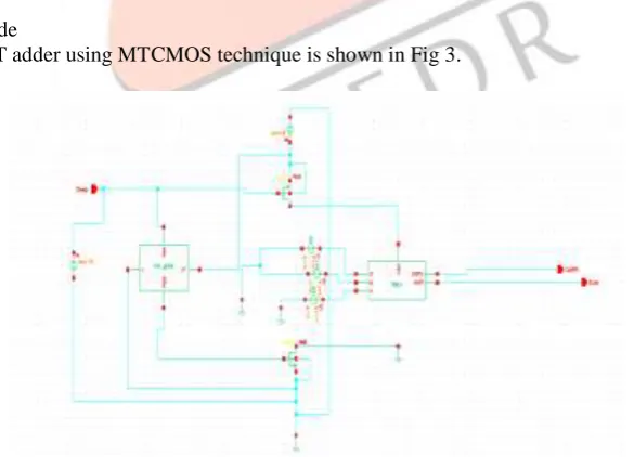
b. One Bit 16T Adder Using MTCMOS Technique
MTCMOS technique uses multiple threshold voltages which is used to optimize delay and power of circuit. High Vth transistors are connected at Vdd and Vss terminal. Circuit uses low Vth transistors.Vth is gate voltage which is at the interface of oxide layer and substrate body. Low Vth transistor is faster and is used to optimize the critical delay path whereas high Vth transistors are used to reduce power
Consumption in standby mode
The schematic of one bit 16T adder using MTCMOS technique is shown in Fig 3.
Fig 3. 16T one bit using MTCMOS Technique
IJEDR1702304
International Journal of Engineering Development and Research (www.ijedr.org)1957
Fig 4: 8 bit conventional adder using 8 full adders(a0,b0,a1,b1…..a7,b7 ) are the binary inputs of RCA,sum0 to sum7 are the output of each adder and carry_out is the output carry .In
RCA each adder provide delay of two logic gates.(2tpd). Hence to connect n bit RCA total delay is 2ntpd.
RCA adder is also known as parallel adder. It’s more accurate and reliable than other adder. The only disadvantage is if the no. bits are increased, speed of operation will be decreased. Cadence schematic of 8 bit conventional full adder with 4 bit full adder is shown below in fig 5.
Fig 5. 8 bit conventional full adder using 4 bit full adder
III. 8 BIT RIPPLE CARRY ADDER USING MTCMOS TECHNIQUE.
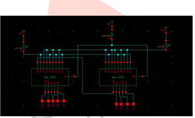
a. Using 4 bit RCA
Two 4bit RCA cascaded to make 8 bit RCA. Carry_out from first 4 bit propagates to carry _in of next 4 bits. Power supply as well as threshold voltage need to be reduced when the transistor size has been scaled As Vth is reduced leakage currents increase exponentially Earlier dynamic power was the major concern but as the need of portable device increased power dissipation at standby mode becomes the major issue. 40% of the total power dissipates at the standby mode. With very large scale integration projects this amount of power dissipation is intolerable. Power dissipation factor dominates over the performance of the circuit. So to overcome this popular technique has been introduced known as MTCMOS. This technique uses two kind of transistor one High Vth which reduces 10 times static power as compare to low Vth whereas low Vth is used to increase the speed of the circuit.
The schematic of 8bit RCA is shown in fig 6.
IJEDR1702304
International Journal of Engineering Development and Research (www.ijedr.org)1958
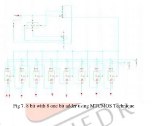
Fig 6. 8 bit full adder with 4 RCA using MTCMOS Techniqueb. Using 8 full adders
8 full adders are cascaded to make 8 bit full adder. This circuit has lower power dissipation as compared to 4 bit cascaded full adder. The cadence schematic is shown in Fig 7.
Fig 7. 8 bit with 8 one bit adder using MTCMOS Technique
IV. Simulation and results:
A conventional adder using 4 bit and 8 full adders, 8 bit using 4 bit and 8 full adders with MTCMOS Technique has been designed with Cadence virtuoso Tool. The power dissipation at static mode reduces to very large extend as per shown in Table 1 using MTCMOS Technique and delay reduces to almost 18% in case of MTCMOS Technique. Hence MTCMOS is a very powerful technique in terms of low power dissipation and delay of the circuit. The simulation values of various parameters are labelled on the output graph of various circuits.
IJEDR1702304
International Journal of Engineering Development and Research (www.ijedr.org)1959
Fig8. Output of 16T using MTCMOS TechniqueFig9. Output of 8 bit with 8 full adders using MTCMOS Technique
b. Static Power Dissipation Graphs :
Static power is dissipated when the device is in off mode i.e. no input is applied to the circuit. As the generations grow the trend of portable devices increases and the main requirement is to run these devices for longer run. This low power dissipation is achieved by MTCMOS Technique and the output graphs of power dissipation at various circuits are shown below
IJEDR1702304
International Journal of Engineering Development and Research (www.ijedr.org)1960
Fig11. 16T Full Adder using MTCMOS TeChniqueFig12. 8 bit with 8 full adders using MTCMOS Technique Table 1 : Comparison of Delay and Power dissipation of various Full Adders
S.No. Different Adder Architectures Dynamic power dissipation(µw)
Static power dissipation (ps)
Delay(ps)
1. 16T One bit full adder 3.989 109.0 177.0
2. 16T One bit full adder using MTCMOS Technique
29.86 4.596 66.65
3. 8 bit conventional full adder using 4 bit RCA
17.14 872.2 9.255
4. 8 bit full adder with 4 bit RCA Using MTCMOS Technique
46.04 4.596 8.576
5. 8 bit with 8 one bit conventional full adder
30.84 872.2 7.469
6. 8 bit with 8 one bit full adder using MTCMOS Technique
39.03 4.596 6.09
CONCLUSION
A RCA using 4 bit and 8 full adders has been proposed by using MTCMOS Technique. The circuit are operated at 1.8V power supply. The static power reduced almost 90% of the conventional Technique and delay also reduced to some extend depends upon the architecture of the circuit. The various simulation results are shown previously. The CMOS has been the leading technology in today’s world of mobile communication due to its low power consumption. Reduction of leakage power in CMOS has been the research interest for the last couple of years. In CMOS integrated circuit design there is an important trade-off between technology scaling and static power consumption. In today’s CMOS technology the leakage power consumption plays a significant role. The main aim of this writing is to give a review of the various steps taken towards the reduction of the leakage power for VLSI designs As Nano-scale design is approaching the total chip power consumption becomes dependent on leakage power.
To solve the problem faced various works have been implemented and still engineers are working on this field. Hence it has been concluded that techniques like MTCMOS is more matured technique to improve speed as well as power consumption of the circuit .Finally it is concluded that the optimized layout will also play an important role in reducing the leakages.
REFERENCES
[1] Nirmal U.,Sharma G.,Mishra Y., “Low Power Full Adder Using MTCMOS Technique”in proceeding of International Conference on Advances in Information,Communication Technology and VLSI Design,Coimbatore, India, August 2010.
[2] Nirmal U.,Sharma G.,Mishra Y.,“ MTCMOS technique to minimize stand-by leakage power in nanoscale CMOS VLSI”, in proceeding of International Conference on System Dynamics and Control,Manipal, India, August 2010.
IJEDR1702304
International Journal of Engineering Development and Research (www.ijedr.org)1961
systems”, IEEE transactions on instrumentation and measurement, Vol.59, No.5, pp.1127-1133.[8] Kalyani P., Satishkumar D.P. and Ragini D.K., 2006, “Various Low Power Techniques for CMOS Circuits, International Journal of Engineering Research and Applications”, pp.2248-9622.
[9] Sharma B.P. and Mehra R., 2014,”High Speed & Power Efficient Inverter using 90nm MTCMOS Technique”,