IJEDR1701113 International Journal of Engineering Development and Research (www.ijedr.org) 716
DESIGN OF RIPPLE CARRY ADDER
USINGQUANTUM-DOT CELLULAR AUTOMATA
Gomathi.V.S
1, Monisha.G
2, Nirmala Shiny Sherin.D
3, Rajat KumarDiwibedi
41,2&3
Student of B.E, Department of Electronics and Communication Engineering, Jeppiaar SRR Engineering College, Chennai.
4
Assistant Professor,Department of Electronics and Communication Engineering, Jeppiaar SRR Engineering College, Chennai.
_____________________________________________________________________________________________________________________
ABSTRACT:
Quantum-Dot Cellular Automata (QCA) is an emerging nanotechnology, with the potential for faster speed, smaller size, and lower power consumption than transistor-based technology. The basic logic circuits of the system are inverter and majority gates. Quantum-Dot Cellular Automata has a simple cell as the basic element. The cell is used as a building block to constructgates and wires. These structures were designed with minimum number of cells by using cell minimization technique. This project utilizes the QCA characteristics to design the Ripplecarry adder. A Ripple carry adder is a logic circuit in which the carry-out of each full adder is the carry-in of the succeeding next most significant full adder. Multiple full adder circuits can be cascaded in parallel to add an N-bit number. The layout of a ripple-carry adder is simple, which allows fast design time. The experimentation with the proposed designs have been successfully verified through the QCADesigner tool.Keywords: Quantum dot cellular automata, Ripple carry adder, Majority gates, QCADesigner ______________________________________________________________________________
I.INTRODUCTION
Transistors cannot get much smaller than their current size once it is fabricated. The area and complexity are the major issues in circuit design. The quantum dot cellular automata can implement digital circuits with faster speed, smaller size and low power consumption, even though the design of logic modules in QCA is not always straightforward. Over several decades Quantum dot Cellular Automata has gained a lot of attention as it offers extremely low power, operation at very high frequency (usually in Tera-Hertz) and high density for implementing any digital logical circuit.
The main motivation of scaling is to provide high performance devices which can operate at very high frequency ranges usually in Tera-Hertz and have low power consumption. In QCA the information storing procedure is different, as position of electrons decide the logic states. Dr. Criag Lent first proposed this novel idea. In the QCA technology the primitive structure is a QCA cell. In this paradigm the QCA cell consists of four quantum dots at the four corners of a square geometry where mobile free electrons are pushed and are confined to any of two quantum dots at the opposite diagonals.
IJEDR1701113 International Journal of Engineering Development and Research (www.ijedr.org) 717 potential wells are located, one in each corner of the QCA cell. In the QCA cells, exactly two electrons are locked in. They can only reside in the potential wells. The potential wells areconnected with electron tunnel junctions. They can be opened for the electrons totravel through them under a particular condition, by a clock signal. Without any interaction from outside, the twoelectrons will try to separate from each other as far as possible, due to the Coulombforce that interacts between them. As a result, they will reside in diagonally locatedpotential wells, because the diagonal is the largest possible distance for them toreside.
2.QCA LOGIC
Coulombic forces will cause adjacent cells to interact. The state of thecells will always tend to the lowest energy. We can take advantage ofthis to transmit information through a “wire” by forcing the polarizationof a cell at one end.
3.QCA CLOCKING
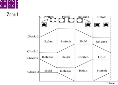
Clock is one of the important features to control CMOS circuits. Similarly QCA circuit is also controlled by clock [1-5]. In order to control the potential barrier which exists when the electrons present in the quantum dots as they try to move along the tunnel junction and another barrier comes into play when switching occurs between the cells. In order to synchronize the flow of information, clocks are necessary. Four different clocking zones are present in QCA clocking
IJEDR1701113 International Journal of Engineering Development and Research (www.ijedr.org) 718 B) Hold phase-As the name of this phase depicts the electrons will be strongly held in their previous position within the cell as polarization remains same as achieved in the last phase.C)Release phase-In this phase QCA cell's polarization is lost and it is converted back into its normal un-polarized state. As a result the obstruction between dots is reduced and the electrons can move through dots.
D) Relax phase–The obstruction between the quantum dots remain as same as obtained in the release phase and therefore the cell's state remains same.
4.QCA CROSSOVER
In designing of QCA circuit sometime it requires to crossover a wire for interconnection of components. Mainly two types of crossover are available, one is multilayer and other is coplanar. In multilayer crossover, multiple layers are used for the interconnection of component. In coplanar crossover method, wire crossing is performed by two different types of cell. One wire has cells with 900 orientation Fig (a) and other wire has cells with 450 orientation Fig (b).
Fig (a) Fig (b)
III.EXISTING WORK
IJEDR1701113 International Journal of Engineering Development and Research (www.ijedr.org) 719
IV.PROPOSED WORK:
This project deals with designing Ripple carry adder circuit using Quantum-Dot Cellular Automata. This design composed of MAJORITY gates to implement the logic structure. Ripple carry adder can be designed by integrating the fulladders.The advantage of using this QCA technology, reduces the size, increases the execution speed with a considerable power consumption.
A.MAJORITY GATES
The basic QCA gate is 3- input majority gate. In it QCA cell is used as a basic building block. The 3- input majority gate can be made by using 5 QCA cells arranged in two different ways.
In 3 input majority gate 3 cell will work as input cells, now the centre cell will be affected by the sum of the coulomb forces of 3 input cells, so the centre cell‟s electrons adjustment will be the majority of the adjustment of 3 input cells. Finally the 5th cell will give the output according to centre cell adjustment. So expression of three input majority gate can be given by (1).
M3(A,B,C)=AB+BC+CA ...(1)
By using three input majority gate we can make AND & OR gate by taking one input as „0‟ or „1‟ as in (2) and (3).
A.B=M3(A,B,0) …(2)
A+B=M3(A,B,1) …(3)
A NOT gate can also be made by QCA cells by inverting the position of electrons in QCA cell , so that input logic „0‟ will result as output „1‟ and input logic „1 will result as output „0‟
Researchers have designed 5- input majority gate based QCA circuits. These are more efficient in terms of area and faster than the previous designs. Some of the 5-input majority gate structures have been presented. The logic function of 5- input majority voter can be expressed below,
M5(A,B,C,D,E)=ABC+ABD+ABE+ACD+ACE+ADE+BCD+BCE+BDE+CDE
IJEDR1701113 International Journal of Engineering Development and Research (www.ijedr.org) 720 Where A, B, C, D, E are 5 inputs and output cell is indicated by „OUT‟. Remaining medium cells are device cells which aggregate the coulombic forces of all input cells and drive it to the output cell.
B.RIPPLE CARRY ADDER
It is possible to create a logical circuit using multiple full adders to add N-bit numbers. Each full adder inputs a Cin, which is the Cout of the previous adder. This kind of adder is called a ripple-carry adder, since each ripple-carry bit "ripples" to the next full adder. Note that the first (and only the first) full adder may be replaced by a half adder (under the assumption that Cin = 0). The layout of a ripple-carry adder is simple, which allows fast design time utilizing efficient five input majority gates; however, the ripple-carry adder is relatively slow, since each full adder must wait for the carry bit to be calculated from the previous full adder. The gate delay can easily be calculated by inspection of the full adder circuit.
IJEDR1701113 International Journal of Engineering Development and Research (www.ijedr.org) 721 V.CONCLUSION
During course of the project much progress has been made on basic logic gates and tested using QCADesigner software. The operation of circuits has been verified using truth table. The basics circuits such as adders, half adders, full adders, subtractor, half subtractor, full subtractor were studied, implemented and verified using QCADesigner. Further using this basic circuits, work has been done and ripple carry adder is designed and output has verified. In this work the design of ripple carry adder uses only less number of gates which reduces the sizes. And this also reduces the power consumption and increase the speed comparing to the CMOS technology.
VI.FUTURE WORK
Planned improvement for future work includes design of multipliers using basic adders and subtractor circuits. Work regarding clocking for stimulation of multipliers circuits has been in progress. And design of various types of multipliers circuits can be designed and implemented from this work. This work can be used to achieve various advantages and development in QCA technology. Further research work can be in this project in future to bring progressive development in VLSI.
REFERENCES
[1] Schaller and R. Robert, Technological innovation in the semiconductor industry:a case study of the International Technology Roadmap for Semiconductors (ITRS).Diss. George Mason University, 2004.
[2] C. S Lent, P. D. Tougaw, W. Porod a nd G.H.Bernstein,“Quantumcellularautomata." Nanotechnology, vol. 4, no.1, pp. 49-57, 1993
[3] S. E. Frost, A. F. Rodrigues, A. W. Janiszewskie, R. T. Rausch and P. M.Kogge, "Memory in motion: A study of storage structures in QCA." First WorkshoponNonSilicon Computing, vol. 2. 2002.
[4] A. Gin. P. D. Tougaw and S. Williams, "An alternative geometry for quantumdotcellular automata." Journal of Applied Physics, vol. 85, no 12, pp. 8281-8286,1999.
IJEDR1701113 International Journal of Engineering Development and Research (www.ijedr.org) 722 1752-1755, 2001.
[6] K. Walus, G. A. Jullien and V. S. Dimitrov, “Computer arithmetic structures forquantum cellular automata." Signals, Systems and Computers, 2004. Conference
Record of the Thirty-Seventh Asilomar Conference on. vol. 2, pp. 1435 1439,2003.
[7] D. A. Antonelli, D. Z. Chen, T. J. Dysart, X. S. Hu, A. B. Khang, P. M. Kogge,R. C. Murphy, nad M. T. Niemier, "Quantum-dot cellular automata (QCA) circuitpartitioning: problem modeling and solutions." Proceedings of the 41st annualDesign Automation Conference. ACM, pp. 363-368, 2004.
[8] N. A. Shah, F. A. Khanday and J. Iqbal, "Quantum-dot Cellular Automata(QCA) Design of Multi-Function Reversible Logic Gate. “Communications inInformation Science and Management Engineering, vol. 2. no. 4, pp.8-18, 2012.
[9]R. Rathi Devi, S. Thilakavathi, K. M. Suganya , “ Clock Zone Based QCAAdder Architecture Design” , International Journal of Advanced Research inComputer Science and Software Engineering , Vol 5, Issue 10, October-2015.
[10]RamanandJaiswal, TrailokyaNathSasamal, “Efficient Design of Exclusive-Or
Gate using 5-Input Majority Gate in QCA International Conference on AdvancedMa terial Technologies (ICAMT)-2016 .
[11]Golijyothirmai, DanthamalaKoteshwarrao, “Adaptive Techniques in VerilogImplementation of Area-Delay Efficient using QCA Binary Adders” , Internationaljournal of scientific engineering and technology reaserach, Vol.04,Issue.29, August-2015.
[12]Subhasheebasu, “Realization of xor and xnor gates using qca basic gates”, International Journal of VLSI and Embedded Systems-IJVES, Vol 05, Article 10473,November 2014.
[13]K.Lavanya,S.Ramanjinaik, “New design approach to implement binary adderby using QCA” , International Research Journal of Engineering and Technology(IRJET) , Volume: 03 Issue: 02 Feb-2016.
[14] Heumpil Cho, Earl E. Swartzlander, “Adder and Multiplier Design in