IJEDR1701070
International Journal of Engineering Development and Research (www.ijedr.org)453
Effect of Tb3+ doping on structural, optical and
electrical behavior of CdSe nanoparticles prepared by
hydrothermal method
1P.Sanjay, 2K.Deepa, and 3S.Senthil,*
1Research Scholar, 2Research Scholar, 3Assistant Professor
1,3Department of Physics, Government Arts College for Men (Autonomous), Chennai-35, India. 2Department of Physics, Loyola College, Chennai-34, India.
________________________________________________________________________________________________________
Abstract -The structural, optical and dielectric properties of the rare earth Terbium (Tb3+) doped CdSe one dimensional
semiconductor nanorods has been explored. The pure and 0.5% Terbium (Tb3+) doped CdSe nanorods were synthesized
by using hydrothermal method at a moderate temperature of 180°C. The prepared samples were characterized by X – ray diffraction, Scanning Electron Microscopy (SEM), Energy Dispersive X–ray diffraction (EDX) analyses. The X–ray
diffraction (XRD) study shows the wurtzite structure for pure and Tb3+ doped CdSe nanorods. The band gap of the pure
and doped CdSe nanorods was found. PL The strong PL intensity confirms a blue shift. The dielectric and electrical
conductivity studies of pure and Tb3+ doped CdSe were carried out.
Key words -Nanoparticles, nanorods, CdSe, Tb3+doped CdSe, SEM, dielectric study.
________________________________________________________________________________________________________ I. INTRODUCTION
The one dimensional semiconductor nanocrystals having unique structural, optical and electrical properties have been considered as structural units for modern electronic devices, sensors, photonic materials. Therefore, several synthetic routes have been employed for production of nanorods and nanowires [1-2]. The chemical synthesis of high quality Cadmium Selenide (CdSe), Cadmium Telluride (CdTe), Zinc Selenide (ZnSe) etc, nanocrystals is now becoming a routine procedure due to the attractive features present in these materials. Cadmium Selenide is one of the key members of the II –VI semiconductor family, to match the maximum range of the solar spectrum and also has high photo sensitivity. CdSe nanorods came to be exciting materials due to some important properties up to 100% polarized photoluminescence [3]. From the environmental perspective solvothermal method is effective than many other synthesis methods.
The complexing agents and the Cd/Se ratio of raw materials play a marked role in controlling the morphology and to obtain rod – like CdSe nanocrystals, a high concentration of CdSe monomers in reaction solution is needed to enhance the nucleation and growth rate. There are numerous techniques for synthesis of CdSe nano rods reported by various authors [4-5]. Evidences are available about exploiting the photo luminescent property of the rare earth elements in II – VI compounds [6-7]. Reports are available about the doping with transition elements in chalcogenides [8-9].
Literature of doping of CdSe with iron (Fe) and Cu/Tb co-doped is also available. In iron doped CdSe, the iron ions occupy highly asymmetric and nearly symmetric lattice side. The chalcogenides nanoparticles doped with rare earth elements posses a large emission –excitation separation and long fluorescence life time. The reports on Tb doped Cds nanoparticles as probe for mercury ions based on quenching of [10] Tb and fluorescent enhancement due to Tb/Cds doped nanoparticles in silica xerogels [11] are also available in the literature. Co-doping of the materials is done to take the benefits of the both foreign impurities to get a novel hybrid material.
There are considerable interest in transition metal doping (Mn, Cu, Co, etc.) of colloidal nanocrystals as a mean of modifying their properties. Also, it is known that Tb has low to moderate toxicity hence the doping may play a significant role in reducing the toxicity of CdSe and there are evidence that rare earth doped semi conductors has improved photo luminescent properties. The prepared nano particles were characterized structurally, optically and electrically using powder X – ray diffraction (XRD), Energy dispersive X– ray (EDX). UV–Vis spectroscopy,Photoluminescence (PL), dielectric and conductivity studies. II.Experimental Procedure
Synthesis of CdSe nanoparticles
IJEDR1701070
International Journal of Engineering Development and Research (www.ijedr.org)454
collected, washed repeatedly with Milli Q– water, ethanol and then dried at 80°C. The Tb3+ doped CdSe also prepared in the same procedure.Characterization techniques
The synthesized pure and Tb3+ doped CdSe nanoparticles were characterized by a X-ray Diffractometer (RICH SIEFERT & CO) with monochromatic CuKα (λ=1.5406 Å) and the spectrum was recorded over the 2θ range of 20◦ – 70◦ by step scanning with a step size of 0.05◦. To examine the morphology of the synthesized nanoparticles SEM analysis was carried out on the JEOL JSM-6390LV SEM fitted with secondary electron detector, and equipped with an attachment for the Energy dispersive X-ray spectroscopy (EDX) to enable elemental composition analysis. UV-Vis absorption spectra and photoluminescence (PL) spectra were recorded for the synthesized samples by using Varian Cary 5E spectrophotometer and Jobinyvon Flurolong-3-11 spectroflurometer respectively.
III. Results and Discussion XRD analysis
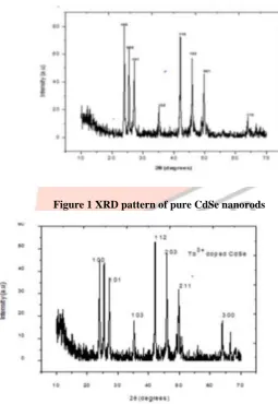
To obtain information on the crystal structure of the pure and Tb3+ doped Cdse nanoparticles X – ray diffraction patterns were recorded. The samples were annealed at 180°C to achieve crystallization. Fig. 1 and Fig. 2 shows the powder XRD pattern of as prepared pure and Tb3+ doped CdSe nanoparticles respectively. All the diffraction peaks from the Tb3+ doped CdSe nanoparticles are consistent with the wurtzite phase. The products are in phases with the calculated lattice constant, a = 4.214 A° and b = 4.219 A° c = 6.904 A°these can be compared with the JCPDS values. The strong and sharp diffraction peaksis observed at 25.8°, the sharp diffraction peaks indicate that the products are highly crystalline. The average grain size (D) of Tb3+ doped CdSe is calculated by the Debye – Scherrer formula, It was found that the average crystalline size of pure and Tb3+ doped CdSe were 25 nm and 30 nm respectively.
Figure 1 XRD pattern of pure CdSe nanorods
Figure 2 XRD pattern Tb3+ doped CdSe nanorods
UV – Vis Spectroscopy
Figure 3and Fig.4 shows the optical absorption spectra of the pure and Tb3+ doped CdSe nano rods. The spectra clearly shows that the broad peaks at 645 nm for pure and at 655 nm for doped CdSe nanorods. After doping with terbium ions the response of CdSe nano rods to visible light was increased and showed blue shift (towards increased wavelength). The blue shift of the absorption curve results in a reduction of the band gap energy. The band gap for pure and doped CdSe nano rods was calculated using the formula
Eg = ℎ𝐶
IJEDR1701070
International Journal of Engineering Development and Research (www.ijedr.org)455
Where, h is planks constant (6.626x10⁻³⁴Js), c isspeed of light (3.0 x 10⁸m/s), λ is cut-off wavelengths. The calculated band gap of pure CdSe is 1.9235eV and Tb3+doped CdSe is 1.894eV. The observed values are greater than the bulk counterpart due to quantum confinement effects.Figure 3 UV-vis absorption spectra of the pure CdSe nanorods
Figure 4 UV-vis absorption spectra of the Tb3+ doped CdSe nanorods
Photoluminescence spectroscopy
The photoluminescence emission spectra of the pure and doped CdSe nano rods were recorded at excitation wavelength of 400 nm at room temperature. The spectra obtained are shown in Fig.5. Sharp peaks were observed at 610 and 724 nm from both the samples. The sharp peak observed at 724 nm confirms a blue shift of the bulk wurtzite terbium doped CdSe. Further the strong PL intensity ascertains the good crystalline quality of the synthesized nano rods. The PL emission spectral study supports the view that the nano particles are predominantly nano rods with uniform size distribution. A slight increase in the excitonic photoluminescence intensities of the spectra Tb3+ and CdSe nano rods samples was observed as compared to their undoped counterpart.
Figure 5 Photoluminescence spectra of the pure CdSe and Tb3+ doped CdSe nanorods
SEM analysis
IJEDR1701070
International Journal of Engineering Development and Research (www.ijedr.org)456
magnification level at 500 nm. Fig. 6 and Fig.7 shows the SEM image of the prepared pure and Tb3+ doped CdSe samples. The solvent hydrazine hydrates (HH) and ammonia (NH3.H2O) is playing an important role in the growth of as formed terbium doped Cadmium selenide nano rods. When the loss of hydrazine is faster, selenide molecules will agglomerate together and condense as rod shaped crystals. Therefore in the synthesis of metal selenide 1D nano structure, several factors such as the reaction temperature and time of heating should be considered..
Figure 6 SEM image of the pure CdSe nanorods
Figure 7 SEM image of Tb3+ doped CdSe nanorods
Energy Dispersive X – ray analysis (EDX)
EDX is an important technique to analyses the composition of elements quantitatively and to solve the chemical identity of metals. The EDX spectra of the synthesis of pure CdSe and Tb3+ doped CdSe nano rods were recorded and they are displayed in Fig. 8 and Fig.9. Fig.8 shows only Cd and Se and no traces of other element. In Fig.9,the peaks confirmthepresence of Tb, Cd and Se metals. From the EDX analysis, it is clear that the obtained products are terbium doped Cadmium selenide.
IJEDR1701070
International Journal of Engineering Development and Research (www.ijedr.org)457
Figure 9 EDX spectra of the Tb3+ doped CdSe nanorods
Dielectric properties
The dielectric studies show the effects of temperature and frequency on the conduction phenomenon in nano structured materials. Dielectric behavior can effectively be used to study the electrical properties of the grain boundaries. The dielectric properties of materials are mainly due to contributions from the electronic, ionic, dipolar and space charge polarizations. The dielectric parameters like the dielectric constant, dielectric loss and the AC conductivity are the basic electrical properties of the Tb3+doped CdSe nano rods. The variation of the dielectric constant, loss and conductivity of the pure and Tb3+ doped CdSe nano rods at frequencies of 50 HZ to 5 MHZ was studied. In conductivity measurements sinusoidal voltage of different frequencies were applied across the sample of thickness d and area A. If ω is the angular frequency of the applied signal (ω = 2πf) and ε0 is the permittivity of free space then AC conductivity is given by,
σᴀᴄ = ω ε0 ε̋ σᴀᴄ = ω ε0 έ tan δ
The real part of dielectric constant is given by ε̋ =𝐶𝑝𝑑
ε0A
The imaginary part of dielectric constant is given as ε̋ =έ tan δ
And, the loss tangent (or) dissipation factor Tan δ =D 1
𝜔𝑅𝑐
The variation of the real and imaginary part of dielectric constant of pure and Tb3+ doped CdSe nano rods as a function of frequency are shown Fig.10 and Fig.11. From the figure the dielectric constant has higher values at lower frequency (50 HZ) and then it decreases to the high frequency (5 MHZ). The dielectric constant is high at lower frequencies is due to the contribution of the electronic, ionic, dipolar and space charge polarization, which depend on the frequencies. Space charge polarization is generally active at lower frequencies and indicates the purity and perfection of the nano particles.
IJEDR1701070
International Journal of Engineering Development and Research (www.ijedr.org)458
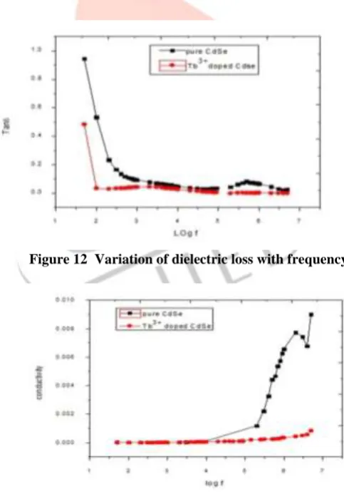
Figure 11 Variation of real part of dielectric constant with frequencyVariation of dielectric loss (tan δ) with frequency for both the CdSe nanorods is shown in Fig. 12. With increasing frequency the value of tan δ is found to be decreasing and is attaining a constant value at higher frequencies. The value of tan δ is to be less for the Tb3+doped CdSe nanorods.
Fig.13. shows the conductivity versus frequency plot for the pureand Tb3+ doped CdSe nano rods. It shows that the value of conductivity is the same for the lower frequencies but at higher frequencies the value of conductivity goes on increasing. The value of conductivity is less for Tb3+ doped CdSe as compared to pure CdSe at higher frequencies. This could be due to large surface scattering which results in a decrease in conductivity and also the short range intrawell hopping of charge carries between localized states but with the addition of terbium the effective number of charge carries involved decreases and thus conducti vity was found to decrease.
Figure 12 Variation of dielectric loss with frequency
Figure 13 Variation of conductivity with frequency Conclusion
IJEDR1701070
International Journal of Engineering Development and Research (www.ijedr.org)459
electrical conductivity of pure and Tb3+ doped CdSe nanoparticles also investigated as a function of frequency at room temperature. It is indicates that the dielectric constant and dielectric loss of the materials decreases with increasing frequency. REFERENCES[1] X. F. Duan, Y. Huang, Y. Cui, J. F. Wang and C. M. Lieber, “Indium Phosphide Nanowires as Building Blocks for Nanoscale Electronic and Optoelectronic Devices”, Nature, vol.409, pp.66-69,2001.
[2] J. D. Holmes, K. P. Johnston, R. C. Doty and B. A. Kor- gel, “Control of Thickness and Orientation of Solution- Grown Silicon Nanowires”, Science, vol.287, pp1471-1473,2000.
[3]G.Ramalingam , N.Melikechi , P.DennisChristy , S.Selvakumar , P.Sagayaraj, “synthesis and Structural, optical property studies of CdSe crystalline nanorods”, Journal of Crystal Growth, vol.311, pp.3138–3142, 2009.
[4] K. Deepa, S. Senthil, S. ShriPrasad and J. Madhavan, “CdS quantum dots sensitized solar cells”, International Journal of ChemTech Research,vol.6,pp.1956-1958 ,2014.
[5] G. Ramalingam and J. Madhavan, “Investigation on the structural and morphological behaviour of CdSe nanoparticles by hydrothermal method”, Archives of Applied Science,vol.3,pp.217-224, 2011.
[6] O.E. Raola, G.F. Strouse, “Synthesis and characterization of Eu-doped cadmium selenide nanocrystals”, Nano Letters,vol.2,pp.1443–1447, 2002.
[7] R.W. Meulenberg, T. van Buuren, K.M. Hanif, T.M. Willey, G.F. Strouse, L.J. Terminello,”Structure and composition of cu-doped CdSe nanocrystals using soft X-ray absorption spectroscopy”, Nano Letters, 4, 2277–2285 (2004).
[8] K.S. Rathore, D.P. Deepika, N.S. Saxena, K.B. Sharma, “Effect of cu doping on the structural, optical and electrical properties of CdS nanoparticles”, Journal of Ovonic Research,vol.5,pp.157–167, 2009.
[9] S.B. Singh, M.V. Limaye, N.P. Lalla, S.K. Kulkarni, “Copper-ion-induced photoluminescencetuning in CdSe nanoparticles”, Journal of Luminescence,vol.128,pp.1909–1912 ,2008.
[10] J. Fu, L. Wang, H. Chen, L. Bo, C. Zhou, J. Chen, “A selective fluorescence probe for
mercury ion based on the fluorescence quenching of terbium (III)-doped cadmium sulfide composite nanoparticles”, Spectrochimica Acta Part A: Molecular and Biomolecular Spectroscopy,vol.77,pp.625–629, 2010.
[11] P. Jyothy, K. Amrutha, J. Gijo, N. Unnikrishnan, “Fluorescence enhancement in