A Control System Retrofit for a Plastic Bag
Making Machine
DR S S ADAMU
Department of Electrical Engineering
Bayero University Kano, Nigeria, PMB 3011 Kano, Nigeria Email: [email protected], phone no: +2348037016383 Abstract
This work presents the development of a microcontroller system to replace a problematic mechanical system of a plastic bag making machine. After detailed study of the existing system the theory of finite state machines is used to model the proposed retrofit, using simulink and stateflow toolboxes of MATLAB. Using the model, the retrofit system is partitioned into hardware and software components. The retrofit is implemented using Microchip’s PIC16F84A 8-bit microcontroller. The developed retrofit performance is the same as the original machine. Due to the flexibility of microcontrollers, other operation and diagnostic features can easily be added
Keywords: retrofit: microcontroller, graphical user interface, weft control
1 Introduction
Plastic technology is a process where plastic materials (usually in chemical form) are processed and shaped into variety of products. The science and technology of plastics has grown to such a prominent level where many products which were once exclusively made from metals, are now being replaced with plastics ones. An example is the PVC pipes used for conduit works in electrical installations are now being used as low cost substitutes for metallic ones. Not surprisingly, many of the finer details of plastic engineering are made possible by control systems: mechanical, electrical and electronics. Precision and automation are now widely employed in the industry.
A locally based company (Cellopack Nig Ltd) has installed some machines to produce many different types of plastic packs. One such system is the plastic bag maker, which in its most elementary form involves cutting and sealing of a plastic film. The data of the machine are given in table 1.
Table 1 Plastic Machine Data
MANUFACTURER S-DAI INDUSTRIAL CO. LTD, TAIWAN, ROC
TYPE SDH-3260 MACHINE NO 1287
DATE OF MANUFACTURE 1991 DATE INSTALLED 1997
The central control system consists of an electronics control card which issues the signal to engage either a clutch or a brake. After working for many years, the control card became a constant source of downtimes: a proposal was made to develop a microcontroller retrofit. The following tasks are defined to achieve the aim:
presents the description of the proposed system. Design and simulation of a state flow model are presented. Construction details and conclusions are presented in sections five and six respectively.
2 Overview of the bag making machine
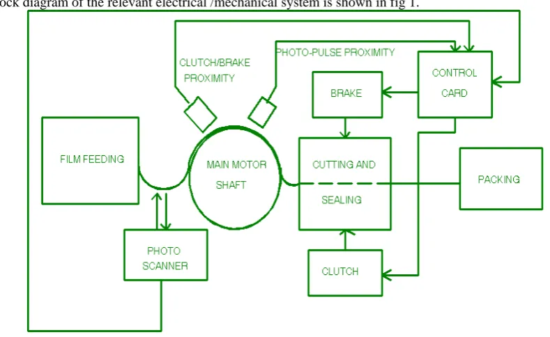
A block diagram of the relevant electrical /mechanical system is shown in fig 1.
Fig 1: Overview of the machine
A roll of plastic film is mounted on feed roller which feeds the film according to size and set tension. Attached to the main motor is a shaft carrying two cams; one for the clutch/ brake proximity and the second for what the manufacturers called “photo_pulse “ proximity sensor.
The function of the clutch cam and its proximity sensor is to deliver a signal to the control card which dictates whether the clutch or the brake is to be engaged. Precisely, a low (0V) signal means the clutch is to be engaged, while a high (12V) signal causes the engagement of the brake. The photo-pulse cam and its proximity sensor are used with a scanner (actually a photo transmitter + receiver unit) to facilitate production of precise cuts on color films. That is, the braking should occur on a marked line on the film. Whenever any of the signals are received by the control card the appropriate solenoid (brake or clutch) is engaged. The clutch pulls the film while the brake stops it for cutting and sealing. At the right end of the machine there is a counter and packaging table for the operators.
2.1 The electrical/electronics system
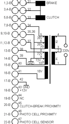
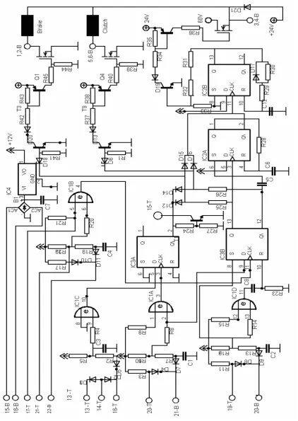
Since the machine had no schematic diagram, it was decided to produce both the cards interface and schematic diagrams from the existing control card. Figs 2 and 3 shows the interface and the card electronics diagram respectively.
Fig 3: Card’s electronics schematic diagram
the
Q
output)goes high. This output now allows normal clutch / brake operation, and also latches on the relay via terminal15-T. From now onward, there are two modes of operation depending on the state of the scanner.(1) Mode 1 – with scanner off
Pin 20-B (clutch / brake proximity sensor input) when high sets the D-flip flop IC3A pin 8 and thus pin 13 (Q output) goes high powering the brake. At the same time, the monostable formed by IC2A is clocked through its CLK input so it begins its timing. The timing period is given by eq. (1) [17]
28 6
7
.
0
C
R
(1) For this case the value is 2.31ms
At the expiration of the time, the monostable IC2A triggers a second monostable formed by IC2B which starts to time out and also send a high dc voltage for approximately 23.1 msec which then dies out leaving the brake engaged with 24V dc applied. This high dc is necessary for the generation of the initial engaging force. When pin 20 goes low (from the cam proximity), a pulse of duration given eq. (2) by [17]
23 8
3
.
0
C
R
(2) which in this case is approximately 1.0 ms, is injected into the reset input of IC3B and so the flip-flop resets. When the
Q
input goes high, it also injects a pulse of duration into IC2B set pin 6, and the above timing is repeated but this time with the clutch engaged.(2) Mode 2 – scanner turn on
With the scanner on, terminal D (pin 9) of IC3B dictates clutch /brake action through the scanner, ONLY if both S and R inputs are low. With D input high, a CLK from the scanner applies the brake. If the D input is low however, clutch will be engaged as described above. Note the bright on switch S2 at terminal 17-T. This is used to invert the pulses from the scanner for printed or transparent film. The proposed retrofit must carry out the above sequences exactly while monitoring the inputs.
3 The Microcontroller Retrofit
Using the findings of section 2 above, the various inputs and outputs are shown in tables 2 and 3.
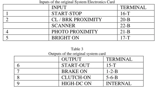
Table 2
Inputs of the original System Electronics Card
INPUT TERMINAL
1 START-STOP 16-T
2 CL / BRK PROXIMITY 20-B
SCANNER 22-B 4 PHOTO PROXIMITY 21-B
5 BRIGHT ON 17-T
Table 3
Outputs of the original system card
OUTPUT TERMINAL
6 START-OUT 15-T 7 BRAKE ON 1-2-B 8 CLUTCH-ON 5-6-B 9 HIGH-DC ON INTERNAL
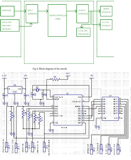
Fig 4: Block diagram of the retrofit
Fig 5: Schematic diagram of the retrofit
From fig 4, the input interface is the same as the in the original system, except for conversion of the 12V level to 5V level using resistive voltage dividers. The system uses “portb interrupt on change” feature [60], to sense the clutch / break proximity transitions. The photo-pulse input is sensed by the RB0 interrupt [60]. The output interface uses a high current Darlington driver to replace the original complementary driver.
4 System Modeling, Design and Analysis
A mathematical model is invaluable in facilitating understanding and allowing further modifications and refinements of any system. From earlier considerations, it is obvious that the system possesses binary inputs and outputs making amenable to analysis using digital techniques
4.1 System Modeling Using State Diagrams
The original system may be modeled using the state diagram approach which was developed in chapter two. The simulink and stateflow toolboxes of MATLAB are used to implement the model. From the original system description, the following states and outputs (actions) are identified:
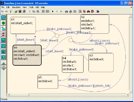
(i) State S0 – the idle state, when the system is not in operation
(ii) State S1 – the start command is given, the main motor is started. Brake is also energized. (iii) State S2 – the control system receives the brake pulse from the cam proximity. The brake is
engaged and the signal for the momentary high dc to the brake is also given.
(iv) State S3 – the time delay for the high dc has elapsed, therefore the high dc signal is off.. (v) State S4 – the control receives the clutch signal (actually the brake pulse go low). The brake
signal is off and the clutch signaled is on. The high dc signal is also activated. (vi) State S5 -. End of high dc signal. Clutch still engaged (material is being pulled).
The control system continues to circled between states S2 and S5, unless a stop signal is received.
4.2 Simulink and Stateflow Model
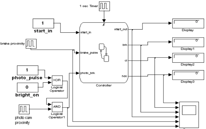
The above states are modeled using MATLAB® toolboxes (simulink® and stateflow®). The Stateflow® is a graphical design and development tool for simulating complex reactive systems based on finite state machine theory, flow diagram notations and state-transition diagrams . It provides a suitable environment for modeling logic system used to control and supervise a physical plant modeled in Simulink. The simulink model of the system is shown in fig 5, while the stateflow diagram of the controller is shown in fig.6.
Fig 6: Stateflow diagram of the controller
The simulink model of the process in fig 5 contains the various objects to simulate the system. Constant blocks are used to simulate various input discrete sensors,, since they are either on or off (0 or 1 in the model). The block labeled “controller” is the stateflow model shown in fig 7.6. The “1 sec timer” simulates the monostable action used to create action delay. The block labeled “brake proximity” is a square wave generator used to simulate the action of rotating motor together with a proximity switch. The blocks labeled “photo pulse, “bright on”, and “photo cam” are used to simulate the operation with a colored material.
The stateflow diagram of fig 7.6 shows the various states as well as the transition lines connecting them. The function after() simulates temporal logic using the events generated by the “1 sec timer” to create the delay required for the high dc output. The various events that can cause a transition are shown adjacent to the transition lines. The sequence of this diagram now follows.
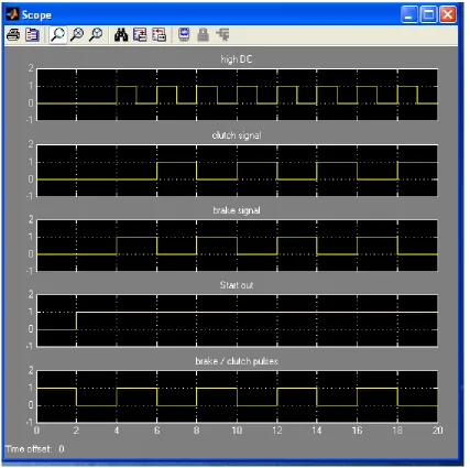
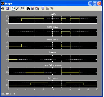
When the system is energized the system will be in state S0, due to the default transition shown (a line with a down arrow into S0). At state S0, all outputs are off. When the start_in signal is received, the system will move to state S1, and also start the motor. The system will move to state S2 when it receives the brake pulse signal from the proximity. At state S2, the outputs; brake signal (brk) and the high dc (hdc) are turned on. The transition out of state S2 has a connective junction which determines which of the two transitions is taken. The stateflow model always evaluates the transition on the labeled transition first. Therefore, in this case, it will first check whether the stop command is given (start_in is low) before taking the alternate transition to state S3. If the start signal is still on, it moves to state S3, where the hdc signal is turned off. When the clutch signal is received (brake pulse low), it moves to state S4, where brk output is turned off and clutch signal (cl) is turned on. At the same time the hdc signal is turned on. After expiry of the time delay, it moves to state S5, where the hdc signal is turned off. When the next brake pulse OR the system receives a signal from the photo circuit, it moves to state S1, and the cycle repeats. The photo circuit consists of the EXOR gate with two inputs to select clear or reverse pattern from the photo sensor, and a photo-cam proximity sensor to time when the brake is to be applied. Figs 7 and 8 showed the results of the simulation without and with the photo cam pulses. It can be seen that the model follow the desired control.
Fig 8: Simulation results for the process with photo cam
4.3 Hardware Design
From fig 3, the input voltage at the inputs of IC1 (a 4070 multiplexer) is +12V, if the proximity is not near the cam. This must be changed to +5V. The input circuitry of the original card together with grounded resistors (U7, U20, U25, U30 and U10) in fig 4 formed a resistive network as shown in fig 9.
Fig 9: Input Interface circuitry
The voltage at the port input is given by
(
K
)
K
)
7
.
4
1
9
.
3
9
.
3
+
+
x 12V = 4.88 VFig 7.11: Interface of retrofit’s ULN2004 to the VMOS FET driver
4.4 Software Development
The flowcharts of the control programs are given in figs 12, 13 and 14.
Fig 13: Interrupt service routine flowchart
Fig 14: Flowchart of the clutch and brake engagement routines
5 Construction and Testing
Fig 15: Top side view of the retrofit
Fig 16: Track side view of the retrofit
The board was then connected to the original card. The card was then subjected to bench tests. This step requires reproduction of the various input voltages and using switches to simulate the proximity and photocells. After these tests the card was then plugged in the slot on the actual machine: its operation was exactly as the original card.
6 Conclusions
to generate C-compiler codes directly. The control retrofit was also realized using a flowchart which was subsequently implemented using a PIC16F84A micro controller.
Trade names
All trade names mentioned in this work belongs to their respective owners
8 References
[1] Adamu S S (2008), “Development of Industrial Retrofits Using Low-Cost Microcontrollers: Case Studies of Four Selected Applications, Unpublished PhD Thesis, Bayero University, Kano
[2] Adam O., “Introduction to Microcomputers, Some Real Products”, Vol. II, Osborne and Associates Inc., June 1977 [3] Horowitz, P. and Hill W., ”The Art of Electronics”, Low Price Edition, Cambridge City, 1995
[4] Protopapas, D. A., “Microcomputer Hardware Design”, Prentice –Hall Inc., 1988
[5] Yacobucci, R.B., “A Control System Retrofit for a GE Frame 5 Turbine/Generator Unit, IEEE Trans on Energy Conversion, Vol.6, No. 2, June 1991
[6] www.tech4.com , “Why Retrofit?”, July, 2004
[7] www.bmuford.com , “A Home Brew CNC Milling Machine”, Dec 1999 [8] www.jtecheng.com , “Obselete Processor Retrofits”, March 2006 [9] www.zetetics.com , “ Software Retrofits”, March 2006
[10] www.greencarcongress.com , “PTT leads Diesel to CNG Conversion”, March 2006 [11] Zimmerman, A. J., ”Fundamentals of Direct Digital Control”, HPAC, May 1996
[12] John G. Bollinger and Neil A. Duffie, “Computer Control of Machines and Processes, Addison-Wesley publishing Company, Reprinted Edition, 1989
[13] Microchip Technology Inc.“PIC16F84A Datasheet-18 Pin Enhanced Flash /EEPROM 8-bit Microcontroller”, 2001 [14] Atmel Corporation, “Three-Wire Serial EEPROM- AT93C56A, AT93C66A Datasheet”, December, 2006 [15] Data Sheet Book, Elector Electronics, 1988
[16] SGS-THOMPSON Microelectronics, “ULN2001A-ULN2004A Datasheets”, 1994