Scholarship@Western
Scholarship@Western
Electronic Thesis and Dissertation Repository
4-10-2012 12:00 AM
Scanning Probe Microscopy Studies of the Properties of
Scanning Probe Microscopy Studies of the Properties of
Conducting Polymers
Conducting Polymers
Kevin D. O'Neil
The University of Western Ontario
Supervisor
Dr. Oleg Semenikhin
The University of Western Ontario Graduate Program in Chemistry
A thesis submitted in partial fulfillment of the requirements for the degree in Doctor of Philosophy
© Kevin D. O'Neil 2012
Follow this and additional works at: https://ir.lib.uwo.ca/etd
Part of the Analytical Chemistry Commons, Materials Chemistry Commons, Physical Chemistry Commons, and the Polymer Chemistry Commons
Recommended Citation Recommended Citation
O'Neil, Kevin D., "Scanning Probe Microscopy Studies of the Properties of Conducting Polymers" (2012). Electronic Thesis and Dissertation Repository. 432.
https://ir.lib.uwo.ca/etd/432
This Dissertation/Thesis is brought to you for free and open access by Scholarship@Western. It has been accepted for inclusion in Electronic Thesis and Dissertation Repository by an authorized administrator of
Scanning Probe Microscopy Studies of the Properties of Conducting
Polymers
(Spine title: Scanning Probe Microscopy Studies of Conducting Polymers)
(Thesis format: Integrated-Article)
by
Kevin D. O‟Neil
Graduate Program in Chemistry
A thesis submitted in partial fulfillment of the requirements for the degree of
Doctor of Philosophy
The School of Graduate and Post-doctoral Studies The University of Western Ontario
London, ON
© Kevin D. O‟Neil 2012
ii
THE UNIVERSITY OF WESTERN ONTARIO
THE SCHOOL OF GRADUATE AND POSTDOCTORAL STUDIES
CERTIFICATE OF EXAMINATION
Supervisor
______________________________ Dr. Oleg Semenikhin
Examiners
______________________________ Dr. Keith Griffiths
______________________________ Dr. Lars Konermann
______________________________ Dr. Lyudmila Goncharova
______________________________ Dr. Michael Thompson
The thesis by
Kevin D. O’Neil
entitled:
Scanning Probe Microscopy Studies of the Properties of Conducting
Polymers
is accepted in partial fulfillment of the requirements for the degree of
Doctor of Philosophy
Date__________________________ _______________________________
iii
ABSTRACT
Electronically conducting polymers (ECPs) have been growing in interest as important materials for a variety of different applications such as charge storage devices and photovoltaics. However, in all of these applications, the performance of conducting polymers are strongly dependent upon their local properties such as morphology, local conductivity and carrier mobility, local chemical composition, etc. All polymer materials feature a distribution of these parameters and therefore, they are considered heterogeneous. In this work, we use atomic force microscopy (AFM) and its related techniques such as current-sensing AFM (CS-AFM), Kelvin probe force microscopy (KFM) and phase imaging (PI-AFM) to directly investigate the heterogeneity of ECPs, specifically poly[2,2‟-bithiophene] (PBT), in order to determine how their performance depends on their local properties and their distribution.
iv
v
CO-AUTHORSHIP
This doctoral thesis has been prepared according to the regulations for an integrated-article format thesis stipulated by the Faculty of Graduate and Postdoctoral Studies at the University of Western Ontario and has been co-authored as follows:
Chapter 3:On the Origin of Mesoscopic Inhomogeneity of Conducting Polymers
All experiments were conducted by K.D. O‟Neil under the supervision of Dr. O.A. Semenikhin. Preliminary studies were started by B. Shaw. A draft of chapter 3 was prepared by K.D. O‟Neil and reviewed by Dr. O.A. Semenkhin. Further edits and revisions were carried out by both K.D. O‟Neil and Dr. O.A. Semenkhin. A copy of this chapter has been published at: O'Neil, K. D.; Shaw, B.; Semenikhin, O. A. Journal of Physical Chemistry B2007, 111, 9253-9269.
Chapter 4: AFM Phase Imaging of Electropolymerized Polybithiophene Films at
Different Stages of Their Growth
All experiments were conducted by K.D. O‟Neil under the supervision of Dr. O.A. Semenikhin. A draft of chapter 4 was prepared by K.D. O‟Neil and reviewed by Dr. O.A. Semenkhin. Further edits and revisions were carried out by both K.D. O‟Neil and Dr. O.A. Semenkhin. A copy of this chapter has been published at: O'Neil, K. D.; Semenikhin, O. A. Journal of Physical Chemistry C2007, 111, 14823-14832.
Chapter 5: AFM Phase Imaging of Thin Films of Electronically Conducting
Polymer Polybithiophene Prepared By Electrochemical Potentiodynamic Deposition
vi
Chapter 6: The Effect of Electropolymerization Method on the Nanoscale Properties
and Redox Behaviour of Poly[2-2’-bithiophene] Thin Film Electrodes
All AFM experiments and characterization were conducted by K.D. O‟Neil under the supervision of Dr. O.A. Semenikhin. Electrochemical experiments on Pt were carried out by A. Forrestal under the supervision of both K.D. O‟Neil and Dr. O.A. Semenikhin. A draft of chapter 6 was prepared by K.D. O‟Neil and reviewed by Dr. O.A. Semenkhin. Further edits and revisions were carried out by K.D. O‟Neil, A. Forrestal and Dr. O.A. Semenkhin. A copy of this chapter has been submitted for publication at: O'Neil, K. D., Forrestal, A., Semenikhin, O.A. Electrochim Acta 2012.
Chapter 7: The Effect of Cycling on the Nanoscale Morphology and Redox
Properties of Poly[2-2’-bithiophene]
vii
ACKNOWLEDGEMENTS
First and foremost, I would like to thank my supervisor, Dr. Oleg Semenikhin.
For the past 5 years, he has always motivated and inspired me to bring out the best in
myself and to never give up and always keep moving forward.
I have also had the honor of having amazing laboratory partners throughout my
time at UWO. Trissa Kantzas, Joshua Byers and Adam Forristal have always been around
to give insight into new ideas, help teach unfamilar concepts or just to have a great
conversation to give our minds a break from research.
Finally, I would like to thank my friends and most importantly, my family. My
father, mother and sister have always been there for me. When times were hard and
stressful, they reminded me of my past and the previous struggles that I always overcame
to continue moving forward. They always took the time to listen and always supported
me in any possible way they could and for that, there are no words to express the
viii
TABLE OF CONTENTS
CERTIFICATE OF EXAMINATION ... ii
ABSTRACT ... iii
CO-AUTHORSHIP ...v
ACKNOWLEDGEMENTS ... vii
TABLE OF CONTENTS ... viii
LIST OF FIGURES ... xiii
LIST OF APPENDICES ... xxiii
LIST OF ABBREVIATIONS ... xxiv
Chapter 1: Introduction ...1
1.1 References ... 4
Chapter 2: Literature Review ...5
2.0 Background ... 5
2.1 Atomic Force Microscopy ... 9
2.1.1 Introduction ... 9
2.1.2 Contact Mode AFM ... 10
2.1.3 Tapping Mode AFM ... 11
2.1.4 Kelvin Probe Force Microscopy (KFM) ... 11
2.1.5 Current-sensing AFM (CS-AFM) ... 16
2.1.6 Phase Imaging AFM (PI-AFM) ... 18
2.2 Structures and Properties of Conducting/Semiconducting Polymers ... 19
2.2.1 Doping ability as Dependent on the Counter-ion Nature... 22
2.2.2 Band Structure of Conducting Polymers ... 23
ix
2.3 Preparation Methods for Conducting Polymers ... 24
2.3.1 Introduction ... 24
2.3.2 Galvanostatic Deposition ... 25
2.3.3 Potentiostatic Deposition ... 26
2.3.4 Potentiodynamic Deposition ... 26
2.4 References ... 27
Chapter 3: On the Origin of Mesoscopic Inhomogeneity of Conducting Polymers ..30
3.1 Introduction ... 30
3.2 Experimental ... 38
3.2.1 Preparation of the Polymer Samples ... 38
3.2.2 KFM and CS-AFM Measurements ... 41
3.3 Results ... 44
3.3.1 “Regular” Polybithiophene (PBT) ... 44
3.3.2 “Nucleated” Polybithiophene ... 54
3.3.3 Spin-Coated MEH-PPV ... 58
3.4 Discussion ... 61
3.5 Conclusions ... 72
3.6 Acknowledgements ... 73
3.7 Supporting Information ... 73
3.8 References ... 74
Chapter 4: AFM Phase Imaging of Electropolymerized Polybithiophene Films at Different Stages of Their Growth ...79
4.1 Introduction ... 79
4.2 Experimental ... 80
x
4.2.2 AFM and Phase Imaging Measurements ... 82
4.3 Results ... 83
4.4 Discussion ... 94
4.5 Conclusions ... 98
4.6 Acknowledgements ... 98
4.7 References ... 98
Chapter 5: AFM Phase Imaging of Thin Films of Electronically Conducting Polymer Polybithiophene Prepared By Electrochemical Potentiodynamic Deposition ...101
5.1 Introduction ... 101
5.2 Experimental ... 103
5.3 Results and Discussion ... 106
5.4 Conclusions ... 114
5.5 Acknowledgments... 115
5.6 References ... 115
Chapter 6: The Effect of Electropolymerization Method on the Nanoscale Properties and Redox Behaviour of Poly[2-2’-bithiophene] Thin Film Electrodes ...116
6.1 Introduction ... 116
6.2 Experimental ... 118
6.2.1 Preparation of Polymer Samples ... 118
6.2.2 Polymer Film Deposition on Pt ... 119
6.2.3 Measurements of Films in Monomer-Free Solution ... 120
6.2.4 Polymer Film Deposition on HOPG ... 120
6.2.5 AFM Measurements of Films on HOPG ... 121
6.3 Results ... 122
6.3.1 Electrochemical CV Characterization ... 122
xi
6.3.3 AFM Characterization ... 130
6.4 Discussion ... 134
6.5 Conclusions ... 138
6.6 Acknowledgements ... 139
6.7 References ... 139
Chapter 7: The Effect of Cycling on the Nanoscale Morphology and Redox Properties of Poly[2-2’-bithiophene] ...142
7.1 Introduction ... 142
7.2 Experimental ... 142
7.2.1 Preparation of Polymer Samples ... 142
7.2.2 Polymer Film Deposition and Characterization on HOPG ... 143
7.2.3 AFM Measurements of Films on HOPG ... 144
7.3 Results ... 145
7.3.1 Changes in the Redox Behavior of PBT Films in the course of Potential Cycling ... 145
7.3.2 AFM Imaging of PBT Films Cycled to Various Potential Limits ... 151
7.4 Discussion ... 154
7.5 Conclusions ... 157
7.6 Acknowledgements ... 157
7.7 References ... 157
Chapter 8: Conclusions ...160
APPENDICES ...163
Supporting Information for Chapter 3: The effect of the molar volume on the polymer nucleation according to the Kelvin model ... 163
Copyright Release from Publisher for Chapter 3 ... 167
xii
xiii
LIST OF FIGURES
Figure 2.1. Molecular structures of (a) poly(3-hexylthiophene) (P3HT) (b) poly[2-methoxy-5-(2-ethyl-hexyloxy)-1,4-phenylene-vinylene]
(MEH-PPV) and (c) poly[2-2‟-bithiophene] (PBT). ...8
Figure 2.2. Basic Schematic of Atomic Force Microscopy (AFM) (adopted from [21]) ...9
Figure 2.3. Explanation of the surface potential measurements. The feedback voltage cancels out the electric field between the tip and the sample when it is equal to the contact potential difference. ...13
Figure 2.4. A basic schematic of phase imaging AFM (PI-AFM) as the probe “taps” over a sample of varying hardness. ...18
Figure 2.5. Molecular structure of polyacetylene ...20
Figure 2.6. Molecular structure of polybithiophene in the aromatic state (top) and quinoidal state (bottom). ...21
Figure 2.7. A representative cyclic voltammogram (CV) of polybithiophene (PBT) in a solution of supporting electrolyte without the monomer showing the process of doping/undoping. ...21
Figure 2.8. The reaction mechanism for the doping/undoping of polybithiophene (PBT). In this reaction (and this work), PF6- is used to maintain electroneutrality (see below). ...22
Figure 2.9. The evolution of the band structure in polybithiophene (PBT). ...23
Figure 2.10. Polymerization of polybithiophene through a non-living radical mechanism. A new radical must be created electrochemically after each radical coupling step in order to continue polymerization. ...25
Figure 2.11. A typical cyclic voltammogram illustrating the potentiodynamic synthesis of polybithiophene. Every subsequent scan results in the deposition of more polymer onto the surface of the electrode (red arrows). ...26
xiv
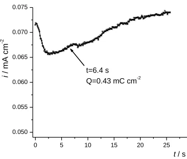
the deposition was terminated (t = 6.4sec) in order to obtain a “nucleated” polymer sample. ...41
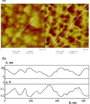
Figure 3.2. (a) Simultaneous 500 nm by 500 nm images of topography (left) and surface potential (right) acquired in the KFM feedback mode for a “regular” polybithiophene sample. The Z-scale was 200 nm (topography) and 0.5 V (surface potential). (b) Dual cross-section of the images of Fig. 4.2a indicating variations in the height (top) and surface potential (bottom) along the same line shown in the images. ...46
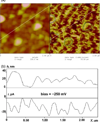
Figure 3.3. (a) Simultaneous 2 μm by 2 μm images of topography (left) and CS-AFM current (right) for the same “regular” polybithiophene sample as in Fig. 3.2. The Z-scale was 200 nm (topography) and 50 pA (current). An external bias of -250 mV was applied. To better indicate the correlation between the topography and CS-AFM current, the contours of a few grains from the topography image are repeated in the current image. (b) Dual cross-section of the images of Fig. 3.3a indicating variations in the height (top) and CS-AFM current (bottom) along the same line shown in the images. ...47
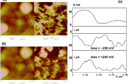
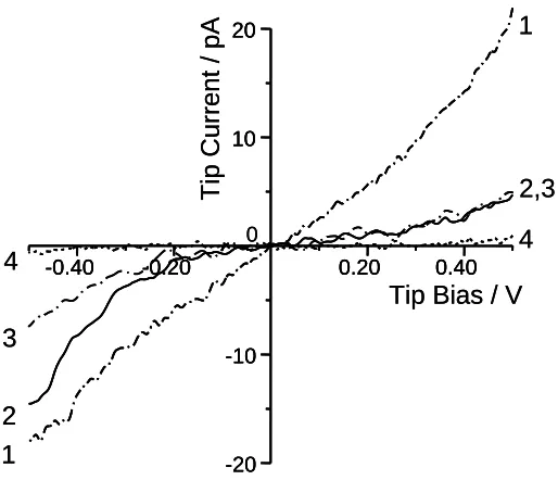
Figure 3.4. (a) Simultaneous 1μm by 1μm images of topography (left) and CS-AFM current (right) for the same “regular” polybithiophene sample as in Fig. 3.2. The Z-scale was 100 nm (topography) and 30 pA (current). An external bias of -250 mV was applied. (b) The image of the same portion of the surface as in Fig. 4.4a taken in identical conditions except that an external bias of +250 mV was applied. (c) Dual cross-section of the images of Fig. 3.4a and Fig. 3.4b indicating variations in the height (top) and CS-AFM current (bottom) along the same line shown in the images. To better indicate the correlation between the topography and CS-AFM current, the contours of a few grains from the topography images are repeated in the current images. ..50
xv
Curve 2 and 4 correspond to semiconducting and insulating areas (grain periphery) of the “regular” PBT samples. See text for further discussion. ...52
Figure 3.6. (a) Simultaneous 500 nm by 500 nm images of topography (left) and surface potential (right) for a “nucleated” polybithiophene sample. The Z-scale was 50nm (topography) and 0.2 V (surface potential). The contours of a few grains from the topography image are repeated in the surface potential image. (b) Dual cross-section of the images of Fig. 3.6a indicating variations in the height (top) and surface potential (bottom) along the same line shown in the images. ...55
Figure 3.7. (a) Simultaneous 1 μm by 1 μm images of topography (left) and CS-AFM current (right) for the same “nucleated” polybithiophene sample (figure 3.6). The Z-scale was 40 nm (topography) and 40 pA (current). An external bias of -500 mV was applied. (b) Dual cross-section of the images of Fig. 3.7a indicating variations in the height (top) and CS-AFM current (bottom) along the same line shown in the images. ...57
Figure 3.8. (a) Simultaneous 500 nm by 500 nm images of topography (left) and surface potential (right) for an MEH-PPV sample spin-coated onto HOPG. The Z-scale was 5 nm (topography) and 0.03 V (surface potential). The contours of a few grains from the topography image are repeated in the surface potential image. (b) Dual cross-section of the images of Fig. 3.8a indicating variations in the height (top) and surface potential (bottom) along the same line shown in the images. ...60
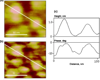
Figure 4.1. Simultaneous 1 μm by 1 μm images of topography (left) and phase (right) for a “nucleated” polybithiophene sample terminated at a deposition charge of 0.07 mC cm-2. The Z-scale was 15 nm (topography) and 40° (phase). ...84
xvi
4.2a and 4.2b indicating variations in the height (top) and phase (bottom) along the same line shown in the images. ...85
Figure 4.3. Simultaneous 1 μm by 1 μm images of topography (left) and phase (right) for a “nucleated” polybithiophene sample terminated at a deposition charge of 1.2 mC cm-2. The Z-scale was 15 nm (topography) and 40° (phase). ...86
Figure 4.4. Enlarged images of (a) topography and (b) phase for the “nucleated” polybithiophene sample shown in Fig. 4.3. The Z-scale was 3 nm and 30°, respectively. (c) Dual cross-section of the images of Fig. 4.4a and 4.4b indicating variations in the height (top) and phase (bottom) along the same line shown in the images. ...87
Figure 4.5. Simultaneous 1 μm by 1 μm images of topography (left) and phase (right) for a “nucleated” polybithiophene sample terminated at a deposition charge of 5.7 mC cm-2. The Z-scale was 30 nm (topography) and 60° (phase). ...88
Figure 4.6. Enlarged images of (a) topography and (b) phase for the larger grains from the second layer of the “nucleated” polybithiophene sample shown in Fig. 4.5. The Z-scale was 50 nm and 60°, respectively. (c) Dual cross-section of the images of Fig. 4.6a and 4.6b indicating variations in the height (top) and phase (bottom) along the same line shown in the images. ...89
Figure 4.7. Enlarged images of (a) topography and (b) phase for the grains from the first layer of the “nucleated” polybithiophene sample shown in Fig. 4.5. The Z-scale was 50 nm and 80°, respectively. (c) Dual cross-section of the images of Fig. 4.7a and 4.7b indicating variations in the height (top) and phase (bottom) along the same line shown in the images. ...90
xvii
Figure 4.9. Enlarged images of (a) topography and (b) phase for the “thick” polybithiophene sample shown in Fig. 4.8. The Z-scale was 100 nm and 80°, respectively. (c) Dual cross-section of the images of Fig. 4.9a and 4.9b indicating variations in the height (top) and phase (bottom) along the same line shown in the images. ...92
Figure 4.10. (a) Simultaneous 1 μm by 1 μm images of topography (left) and surface potential (right) for a “nucleated” polybithiophene sample terminated at a deposition charge of 5.7 mC cm-2. The Z-scale was 40 nm (topography) and 0.1 V (surface potential). (b) Dual cross-section of the images of Fig. 4.10a indicating variations in the height (top) and surface potential (bottom) along the same line shown in the images. ...93
Figure 5.1. (a) A typical cyclic voltammogram of potentiodynamic PBT deposition onto the surface of a highly oriented pyrolitic graphite (HOPG) electrode. The potential scan rate was 100 mV s-1. (b) A typical chronoamperometric curve of potentiostatic PBT deposition onto HOPG. The deposition potential was +1.45 V. ...104
Figure 5.2. Simultaneous 1 µm by 1 µm images of topography (left) and phase (right) for: (a) Potentiodynamically deposited PBT sample after 1 scan cycle. (b) Potentiodynamically deposited PBT sample after 4 scan cycles. (c) Potentiodynamically deposited PBT sample after 10 scan cycles. (d) Potentiostatically deposited “thin” PBT sample (thickness ca. 10 nm). (e) Potentiostatically deposited “thick” PBT sample (thickness ca. 25 nm). For images A-C, the Z scales were 40 nm (topography) and 50 (phase). For images D and E, the Z scales were 20 nm and 100 nm (topography) and 50 and 80(phase), respectively. ...109
xviii
The Z-scale was 150 nm (topography) and 50 (phase). (c) Potentiostatically deposited “thin” PBT sample (thickness ca. 10 nm). The Z-scale was 20 nm (topography) and 50 (phase). (d) Potentiostatically deposited “thick” PBT sample (thickness ca. 25 nm). The Z-scale was 100 nm (topography) and 80 (phase). For all images, dual cross sections are also shown indicating variations in height (top) and phase (bottom) measured simultaneously along the white lines drawn across the same area for each sample, as indicated in the topography and phase images. ...111
Figure 6.1. (a) Typical cyclic voltammograms of “thick” polybithiophene films deposited (1) potentiostatically at a potential of 1.3 V, (2) potentiostatically at a potential of 1.25 V and (3) potentiodynamically by scanning to a maximum potential of 1.4 V for 7 cycles at a rate of 100 mV•s-1. The deposition charge for film 1 was 85 mC•cm-2
xix
Figure 6.2. Dependencies of (a) doping and (b) undoping charges as well as (c) the charge/discharge recovery rate for potentiodynamically deposited PBT films on the number of undoping cycles. The doping-undoping cycling was performed galvanostatically in solution without the monomer at a current density of 0.634 mA•cm-2
to the maximum potentials of (1) 1.3 V, (2) 1.4 V, (3) 1.45 V and (4) 1.5 V. The films were deposited potentiodynamically over 7 scans between 1.4 V and 0V at a rate of 100 mV•s-1
. The thicknesses of these films are ca. 150 nm. ...126
Figure 6.3. Dependencies of (a) doping and (b) undoping charges as well as (c) the charge/discharge recovery rate for potentiostatically deposited PBT films on the number of undoping cycles. The doping-undoping cycling was performed galvanostatically in solution without the monomer at a current density of 0.634 mA•cm-2
to the maximum potentials of (1) 1.3 V, (2) 1.4 V and (3) 1.45 V. The films were prepared at a deposition potential of 1.3V. The thicknesses of these films are ca. 150 nm. ...127
Figure 6.4. Dependencies of (a) doping and (b) undoping charges as well as (c) the charge/discharge recovery rate for potentiodynamically deposited PBT films on the number of doping-undoping cycles. The films were prepared as those in Figure 6.2 and cycled galvanostatically in solution without the monomer at a current density of (1) 0.634 mA•cm-2, (2) 1.268 mA•cm-2, and (3) 2.536 mA•cm-2
to the maximum potential of 1.3 V. The thicknesses of these films are ca. 150 nm. ...128
Figure 6.5. Dependencies of (a) doping and (b) undoping charges as well as (c) the charge/discharge recovery rate for potentiostatically deposited PBT films on the number of doping-undoping cycles. The films were prepared at a deposition potential of 1.3 V and cycled galvanostatically in solution without the monomer at a current density of (1) 0.634 mA•cm-2, (2) 1.268 mA•cm-2, and (3) 2.536 mA•cm-2
xx
the maximum potential of 1.3 V. The thicknesses of these films are ca. 150 nm. ...129
Figure 6.6. (a,b,c) Simultaneous 1 µm by 1 µm AFM images of topography (left) and phase (right) for PBT films deposited potentiodynamically on an HOPG substrate by scanning to a maximum potential of 1.45 V for (a) 1 cycle, (b) 4 cycles, and (c) 10 cycles at a rate of 100 mV•s-1. (d,e) The same images for PBT films deposited potentiostatically on an HOPG substrate at a potential of 1.45 V at a charge of (d) 0.71 mC•cm-2
and (e) 2.9 mC•cm-2. For images a-c, the Z scales were 40 nm (topography) and 50⁰ (phase). For images d and e, the Z scales were 20 nm and 100 nm (topography) and 50⁰ and 80⁰ (phase), respectively. The thicknesses of the films were (a) 12 nm, (b) 40 nm, (c) 60 nm, (d) 16 nm, and (e) 25 nm. ...131
xxi
the anodic scan limit of 1.5 V. One quasi-isosbestic point on the direct scan is located at A (ca. 1.0 V). One special point is observed on the reverse scan located at B (ca. 0.75 V) and one quasi-isosbestic point is seen at C (ca. 0.5 V). All samples were prepared under galvanostatic conditions at a current density of 1 mA cm-2 for 50 s. All CVs were recorded after every fifth scan cycle. ...146
Figure 7.2. The evolution of charges for the samples in fig. 7.1 (a-d) calculated for quadrants 1 (), 2 (), 3(), 4() and 5 () as well as the total anodic () and cathodic () charges to the anodic scan limits of (a) 1.3 V, (b) 1.4 V, (c) 1.45 V and (d) 1.5 V. An exception to this is (a) in which there is no defined quadrant 2 and the total anodic charge is represented by quadrant 1. ...149
Figure 7.3. A plot of the reversible undoping charge (Qr) as well as the irreversible charge loss (IrrQ) versus the number of cycles for the anodic scan limits of 1.3 V (,), 1.4 V (,), 1.45 V (,), and 1.5 V (,). The fully colored shape represents the Qr and the half colored shape represents the IrrQ for their corresponding anodic scan limits. ...150
Figure 7.4. Simultaneous 1 µm by 1 µm images of the topography (left) and phase (right) for polybithiophene films deposited on an HOPG substrate for (a) as-prepared, non-cycled, (b) subjected to 50 doping and undoping cycles to the anodic potential limit of 1.4 V, (c) subjected to 50 doping and undoping cycles to the anodic potential limit of 1.45 V, and (d) subjected to 100 doping and undoping cycles to the anodic potential limit of 1.45 V. All samples were prepared under galvanostatic conditions at a current density of 1 mA cm-2 for 50 s. ...151
xxii
xxiii
LIST OF APPENDICES
Supporting Information for Chapter 3: The effect of the molar volume on the polymer nucleation according to the Kelvin model...163
Copyright Release from Publisher for Chapter 3...167
Copyright Release from Publisher for Chapter 4...168
xxiv
LIST OF ABBREVIATIONS
AC Alternating current
AcN Acetonitrile
AFM Atomic force microscopy
BT 2-2‟ bithiophene
CPD Contact potential difference
CS-AFM Current-sensing atomic force microscopy
CV Cyclic voltammogram
DC Direct current
ECP Electronically conducting polymer
EFM Electrical force microscopy
FFT Fast fourier transform
HOMO Highest occupied molecular orbital
HOPG Highly oriented pyrolitic graphite
KFM Kelvin probe force microscopy
LUMO Lowest unoccupied molecular orbital
MEH-PPV Poly[2-methoxy-5-(2‟ethyl-hexyloxy)-1,4-phenylene vinylene]
Mw Molecular weight
OLED Light emitting diode
xxv
PA Polyacetylene
PBT Polybithiophene; poly[2,2‟-bithiophene]
PI-AFM Phase imaging atomic force microscopy
PT Polythiophene
RR Regioregular
SCE Standard calomel electrode
STM Scanning tunneling microscopy
T Thiophene
TBAPF6 Tetrabutylammonium hexafluorophosphate
Chapter 1: Introduction
Virtually all materials naturally have some degree of inhomogeneity, or in other words, they are considered heterogeneous. When designing a material for applications, micro- and nanostructure and the corresponding nanoscale heterogeneity of the material play an enormous role. Without addressing this key issue, it is impossible to create a material that will be effective for a specific purpose or furthermore, be able to improve a material in order to increase its efficiency.
This apparent heterogeneity is extremely important in the field of electronically conducting polymers (ECPs) for use as organic semiconductor devices such as solar cells or charge storage devices1-3. In these devices, the polymer layer can vary from ten to several hundreds of nanometers in thickness. At this scale, any disorder caused from heterogeneity has a direct impact on the properties and overall performance of these materials. Specifically, the effects of inhomogeneity are directly related to the charge transport efficiency in these materials, which is a crucial parameter for solar cells or batteries. Therefore, there is an interest in investigating the origin of the heterogeneity of these materials and the related effect of this heterogeneity on their properties.
Recent advances in the field of scanning probe microscopy, specifically atomic force microscopy (AFM) have provided researchers with a new powerful tool for visually characterizing the micro- and nanoscopic inhomogeneity, which will be referred to as the mesoscopic inhomogeneity, of ECPs. The mesoscopic scale can be understood as the length scale at which one can study the properties of a material without having to consider the properties of individual atoms. Importantly, this scale (5-500 nm) is also the size of the typical morphological features of most ECPs.
include: current-sensing AFM (CS-AFM), which can determine local electrical properties and, specifically, local conductivity; Kelvin probe force microscopy (KFM), which can be used to assess the local work function of materials and, through it, the chemical composition and the oxidation degree; and phase imaging AFM (PI-AFM), which can determine local mechanical properties and, in particular, local crystallinity. Again, it is important to note that all of these parameters are acquired simultaneously with the topography and therefore these techniques are especially useful in exploring correlations or the lack thereof between the sample morphology and local chemical or electrical properties. The presence or absence of such correlations is important for determining the origin of various nanoscale morphological features and the relation to local electrical and structural properties and whether or not such properties can be controlled through modification in the polymer morphology, for instance, through the use of different deposition techniques.
Most studies on ECPs using AFM have been focused on characterizing just the morphological features of these materials. However, the inhomogeneity of ECPs should not solely depend to their apparent morphological features but should also extend to their local internal properties such as conductivity, oxidation degree, crystallinity, etc. In this work, we utilize AFM and its extensions to study the origin and effect of the heterogeneity of ECPs and relate their local properties and their distribution to the performance of these materials in various devices. The majority of the studies were performed with polymers of the polythiophene series and specifically poly[2,2‟-bithiophene] (PBT), which is a typical conducting polymer and an excellent model system; however, some other important polymers such as poly[2-methoxy-5-(2 -ethyl-hexyloxy)-1,4-phenylene vinylene] (MEH-PPV) were investigated as well.
Chapter 4 describes our early study of the origin of mesoscopic inhomogeneity of conducting polymer films, such as polybithiophene (PBT) and poly[2-methoxy-5-
(2-ethyl-hexyloxy)-1,4-phenylene vinylene] (MEH-PPV), prepared by
correlation between the polymer morphology, the local work function (which is related to the polymer oxidation degree) as well as polymer conductivity is found. In order to explain this correlation, a model is proposed that relates the observed inhomogeneity to preferential deposition of polymer molecules with higher molecular weight at the early stages of the polymer phase formation.
In Chapter 5, we further strengthen our proposed model of the polymer inhomogeneity by studying the nucleation and growth of conducting polymer films5 using AFM phase imaging. It was found that, at the early stages of the polymer nucleation and growth, the polymer films were predominantly crystalline. At the later stages, the polymer contained both crystalline and amorphous phases, with the crystalline polymer located in the grain cores and the amorphous phase found at the grain periphery. It was found that these results are in remarkable agreement with the results of the KFM and CS-AFM measurements from the previous chapter, which relates such inhomogeneity to the presence of both high and low molecular weight polymer fractions (polydispersity) in the electropolymerization solution during deposition.
Chapter 6 focuses on the effect of the electropolymerization method used when preparing conducting polymer films6. In this chapter, the properties of polymer films made under potentiostatic and potentiodynamic conditions were compared using AFM and AFM phase imaging (PI AFM). It was found that while the morphologies of the films prepared using the two techniques were quite similar, the phase contrast measurements revealed a profound difference in the mechanisms of potentiostatic and potentiodynamic electropolymerization, as well as in the nanoscale crystallinity and grain structure of the resulting polymer films and that these differences were especially pronounced at the early deposition stages.
processes approaching 100% over multiple cycles in comparison to potentiostatically prepared films. This was related to the difference in the nanoscale morphology, crystallinity and degree of disorder of polymer films, as evidenced by AFM and PI-AFM.
Finally, chapter 8 further develops the work performed in chapter 7 by characterizing the morphology and crystallinity of conducting polymer films using AFM and PI-AFM after they have been subjected to repeated charging-discharging cycles in order to explain the mechanism of the polymer film degradation and to how to effectively prepare these materials in order to increase the efficiency for use in charge storage devices8.
1.1 References
(1) Schwartz, B. J. Annual Review of Physical Chemistry2003, 54, 141-172. (2) Hoppe, H.; Sariciftci, N. S. Journal of Materials Chemistry2006, 16, 45-61. (3) Novak, P.; Muller, K.; Santhanam, K. S. V.; Haas, O. Chemical Reviews1997,
97, 207-281.
(4) O'Neil, K. D.; Shaw, B.; Semenikhin, O. A. Journal of Physical Chemistry B
2007, 111, 9253-9269.
(5) O'Neil, K. D.; Semenikhin, O. A. Journal of Physical Chemistry C2007, 111, 14823-14832.
(6) O'Neil, K. D.; Semenikhin, O. A. Russian Journal of Electrochemisty.2010, 46, 1345-1352.
(7) O'Neil, K. D., Forrestal, A., Semenikhin, O.A. Electrochimica Acta2012,
Submitted.
Chapter 2: Literature Review
2.0 Background
The field of conducting polymers is very diverse due to the wide range of uses for these materials. As a consequence, the attention of the scientific community is constantly shifting to whichever application will have the greatest impact in the present time. As a result, very often the focus of studies involving conducting polymer inhomogeneity has been based on the needs of specific applications with little attention being paid to developing an overall understanding of where the underlying inhomogeniety of all conducting polymers originates from.
In the 1980-s and 1990s, most studies were focused on the metallic state of conducting polymers. The common polymers studied at the time were mainly polyacetylene, polyaniline and polypyrrole. Electrochemical and related studies of the inhomogeneity of the doping level distribution were initiated at this time as well. Starting in the new millennium, the scientific community began to shift its focus towards semiconducting polymers and applications such as organic light-emitting diodes (OLEDs), organic electronics and plastic solar cells. As a result, studies of the polymer inhomogeneity from the previous generation of conducting polymers were replaced with newer polymers such as polythiophenes and its derivatives such as polybithiophene (PBT) and poly(3-hexylthiophene) (P3HT) (refer to figure 2.1). However, despite the very different functions that polymers such as polyaniline and polypyrrole have in comparison to polythiophenes, the fact remains that these polymers are closely related and therefore, the factors that govern their inhomogeneity should be similar.
summarized in a paper by Prigodin and Epstein6. In this model, it was envisioned that these materials consisted of a network of small, conducting/crystalline domains or islands separated by an insulating/amorphous matrix. The conducting/crystalline domains would be assembled from regularly packed polymer chains with good interchain overlapping. It was thought that this highly packed configuration would occur randomly and only in certain regions of the polymer matrix while the rest of the polymer matrix would consist of amorphous or less conducting polymer fragments where the chain alignment is poor. As a result, the transport of charge within the polymer involves two mechanisms: metallic-like conductivity within the crystalline regions and hopping or resonance tunneling between these domains6.
The most prevailing point of the Prigodin-Epstein model is that it could explain why conducting polymers cannot be 100% doped and why even in the fully doped state the dominant charge transport mechanism in these materials is still hopping rather than band transport. On the other hand, this model does not provide any insight into the mechanisms and properties that control the formation of the crystalline regions embedded into the amorphous matrix.
Therefore, while the Prigodin-Epstein model of the polymer inhomogeneity was developed to explain the properties of the conducting state of conducting polymers and related materials, its concept of isolated highly ordered domains embedded into a disordered polymer matrix is applicable to reduced/semiconducting polymers as well. This conclusion is especially important from a practical viewpoint since the majority of prospective applications utilizing conducting polymers and related materials make use of their semiconducting rather than conducting properties (OLEDs, organic electronics, solar cells, etc.). In all these applications, the polymer inhomogeneity is likely to play a major role. For example, in organic solar cells, it can be detrimental to both the photogeneration of charges in the polymer phase (doped polymers are very poor semiconductors) and their collection (the inhomogeneity can significantly impede the transport of photogenerated carriers).
Currently, the only way to obtain very ordered and regular materials is to use certain monomers that can be arranged in a specific way during their polymerization. A well-known example is regioregular 3-alkyl substituted polythiophene13,14. These materials were shown15 to spontaneously form microcrystalline domains or lamellae very similar to those described by the Prigodin-Epstein model. As a result, such materials indeed demonstrated superior performance in devices such as solar cells15-19. However, these molecules have their drawbacks, such as reduced interchain interactions, limited potential of chemical and structural modifications, more pronounced charge trapping, etc. Therefore, it is desirable to find a more general solution that would be applicable to all polymer-based materials, not only regioregular polythiophenes. To be able to do this, we need to look beyond the Prigodin-Epstein model and further understand the origins of the polymer inhomogeneity and then ultimately find ways to control it.
All previous studies were based on indirect measurements which could not provide any local and especially nanoscale information. Futhermore, there was no way to relate the measured properties to any specific locations or morphological features of the materials under study.
For this work, we use poly[2-2‟-bithiophene] (PBT) shown in figure 2.1. The reason for this is that PBT is a good model system that possesses all the typical properties of conducting polymers. At the same time, PBT is an extremely versatile polymer that can be prepared using a variety of chemical or electrochemical routes and can feature very diverse properties as dependent on the polymerization mechanism, treatment, etc. Its properties can also be tailored to the needs of specific applications.
2.1 Atomic Force Microscopy
2.1.1 Introduction
Atomic Force Micrscopy is a versatile technique that allows the visual characterization of surface structure and the measurement of numerous crucial sample properties on the nanoscale. It was invented in 1986 by Binning, Gerber and Quate20 to broaden the usefulness of its precursor technique, scanning tunneling micrscopy (STM), by allowing measurements on insulating materials. The first commercial AFM was introduced in 1989.
AFM is rather different from other microscopes in the way that it does not form an image by focusing light or electrons onto a surface like an optical or electron microscope. The AFM physically “feels” a sample‟s surface by rastering over a specified area with a sharp probe building a map of the height of the sample. A laser is deflected off of an AFM cantilever (of which the sharp probe is attached to), and into a photodetector which records the deviations in height as the probe scans over the surface. A general schematic of AFM is shown in figure 2.2. This is then translated by the computer into physical data points to form a corresponding image.
AFM can be performed using two base methods of scanning: contact mode AFM and tapping mode AFM. The important advantage of AFM lies with the availability of related auxiliary techniques, or AFM extensions, which allow determination of a number of important additional parameters simultaneously with the topography scanning and at specific well defined points at the sample surface. The auxiliary techniques used in this work include Kelvin Probe Force Microscopy (KFM), Current-sensing AFM (CS-AFM) and phase imaging AFM (PI-AFM).
2.1.2 Contact Mode AFM
Contact AFM mode operates by scanning a tip attached to the end of a flexible cantilever while monitoring the change in cantilever deflection with a photodiode detector as the tip makes physical contact with the sample. To ensure the best results without damaging the sample, the tip should exert a low (typically attractive) force on the sample, which is lower than the effective force holding the atoms of the sample together. The tip-sample interaction causes the cantilever to bend, which in turn allows the variations in the sample topography to be measured with a very high (sub-nanometer) resolution.
A feedback loop within the system is used to maintain a constant deflection of the cantilever and hence, a constant force between the tip and the sample by vertically moving the scanner at each (x,y) data point. The specific force applied to the sample is maintained through setting a user controlled “set-point” deflection, which determines how strongly the tip interacts with the sample. The force is calculated using Hooke‟s law:
(Eq. 2.1)
where F = force,
k = spring constant of the tip
x = cantilever deflection
The distance the scanner moves vertically at each (x,y) point is stored in the computer and forms a topographic image of the sample surface.
2.1.3 Tapping Mode AFM
Tapping mode AFM allows for high resolution topographic imaging of samples that are easily damaged or difficult to image by other AFM techniques such as contact mode AFM. It works by oscillating the cantilever at or near the cantilever‟s resonant frequency using a piezoelectric crystal. The motion caused by the piezoelectric crystal forces the cantilever to oscillate with a high amplitude when the tip is not in contact with the surface of the sample. As the oscillating tip is moved towards the sample, an intermittent contact is established (the tip “taps” the surface). As a result, the oscillation amplitude is reduced due to an energy loss caused by the tip contacting the surface. This change in the oscillation amplitude is utilized to identify and measure surface features in much the same way as the cantilever deflection is used in contact-mode AFM. Specifically, a feedback loop maintains a constant root mean square (RMS) of the oscillation signal acquired by the photodiode detectors in order to achieve a constant tip to sample interaction during imaging.
2.1.4 Kelvin Probe Force Microscopy (KFM)
an AC voltage is applied between the tip and the sample. In this case, there will be a coulombic force between the tip and the sample at the AC voltage frequency, which will be proportional to the amplitude of the AC voltage and the DC potential difference between the sample and the tip. This will cause the cantilever to vibrate at the same frequency, which will be detected in the usual way. In surface potential measurements, there is an additional feedback loop that adjusts the dc voltage on the tip until the vibration of the cantilever is cancelled out (figure 2.3).
This procedure can be illustrated as follows. The energy of a parallel plate capacitor, U, is given by:
2 ) ( 2 1 V C
U (Eq. 2.2)
where C is the local capacitance between the AFM probe and the sample and ∆V is the voltage difference. The force between the tip and sample is the rate of change of the energy with the separation distance:
2 ) ( 2 1 V dZ dU
F (Eq. 2.3)
In the operation of surface potential, the voltage difference, ∆V, consists of both DC and AC components. The AC component is applied from the oscillator, VACsint, where ω is the resonance frequency of the cantilever:
V VDC VACsint (Eq. 2.4) Parameter ∆VDC includes applied DC voltages (from the feedback loop or
externally applied), work function differences, etc. Squaring ∆V and using the relation: 2sin2x = 1 – cos(2x), we get:
2 2 2 ) sin ( sin
2 V V t V t
V
V DC DC AC AC
) 2 2 cos( 4 1 sin ) 2 1 ( 2
1 2 2 2
V t
dZ dC t V V dZ dC V V dZ dC
F DC AC DC AC AC (Eq. 2.6)
The first term is the DC term, the second is the term at the frequency ω and the third is the term at the frequency 2ω. Only the oscillating electric force at ω acts as a sinusoidal driving force that can excite periodic motion of the cantilever (the cantilever responds only to forces at or near its resonance). The goal of the surface potential feedback loop is to adjust the voltage on the tip until it equals the voltage of the sample (∆V= 0), at which point, as follows from (Eq. 2.6), the cantilever amplitude should be zero (Fω = 0).
The DC voltage that is applied to cancel this effect is the same as the contact potential difference (CPD) between the tip and the sample. At this point, the voltage at the tip is the same as the surface potential of the sample so there is no dc electric field between the tip and the sample. This CPD can be used to determine the local work function of the sample and from this, an image of the surface potential and its correlation with the topography can then be obtained.
Figure 2.3. Explanation of the surface potential measurements. The feedback voltage cancels out the electric field between the tip and the sample when it is equal to the contact potential difference.
reduction. This correlation is important for conducting polymers because oxidation-reduction, also called doping/undoping, is known to drastically change the polymer properties. Specifically, doped (oxidized) polymers are conducting, while undoped (neutral) polymers are insulating or semiconducting. Therefore, mapping the variations in the surface potentials allows us to determine the doping-level distribution in conducting polymers with nanometer resolution.
The KFM technique can be also used without engaging the feedback loop. In this mode, called Electrical Force Microscopy (EFM), there is no nullifying bias applied and the tip senses the vertical gradient of the local electric field. However, the data acquired in this mode are very much prone to artifacts due to a pronounced cross-talk between the morphology and the measured electric field (e.g., sharp morphological features will augment the local electric field), so it is less used. In this work, we used only the KFM feedback mode, which is considered to be free of such cross-talk.
sample and the tip by using a bias of the opposite sign. As a result, the surface potential values as measured by the system will lack any physical meaning, which, however, may not be apparent from the images.
The Veeco instrumentation manual recommends setting the drive phase parameter at certain negative values, varying from 0 to -70 degrees for high-frequency cantilevers. Our experience is that this setting does not necessarily work properly. Therefore, in this study, we have always performed additional checks by temporarily switching the output from the surface potential to the so-called surface potential input, which is essentially the raw DC potential difference sensed by the tip. If the feedback is working properly, the contact potential difference between the tip and the sample should be totally compensated, and the values of the potential input should be zero. If this was not the case, the driving phase parameter was adjusted until the proper feedback operation was restored.
As far as can been seen with literature, the first studies that involved KFM (as an extension to AFM) to study the inhomogeneity of polymers was by Semenikhin et al23,24. In these studies, it was found that electrochemically prepared neutral and p-doped films of the conducting polymer, polybithiophene, showed a pronounced non-uniform doping-level distribution. In addition, it was found that the doping-doping-level distribution showed a remarkable correlation with the surface morphology of the polymer. More doped regions of the polymer appeared on the top of polymer grains whereas the grain periphery was found to be less doped. Later, these results were corroborated by other studies24-27.
case, it is more advantageous to corroborate the results found using KFM measurements with results obtained using other independent techniques, such as current-sensing AFM (CS-AFM) and phase imaging AFM (PI-AFM).
2.1.5 Current-sensing AFM (CS-AFM)
CS-AFM is a technique that allows one to measure, in addition to the surface morphology, the local current flowing between the conducting tip and the area of the sample it is in contact with. Since there should be a direct electrical contact between the tip and the sample, CS-AFM images are acquired in the AFM contact mode rather than in tapping mode as with KFM measurements. CS-AFM images are obtained by applying a bias, which is a changeable parameter, between the sample and a conducting cantilever tip, which is set to be on a virtual ground. As the tip runs along the surface of the sample, a linear amplifier with a range of 1 pA to 1 μA senses the current passing through the sample, which then allows an image of the local current and thus the sample conductance to be obtained. Since conducting polymers can vary their conductivity by several orders of magnitude as dependent on their doping level, measuring the local conductivity is yet another way to characterize the variations in the polymer doping level. Unlike other electrical characterization techniques such as scanning tunneling microscopy (STM), CS-AFM does not rely on conductivity as the source of the topographical information. Therefore, it can be used for poorly conducting samples such as semiconducting conjugated polymers.
nm, however, the low quality of the images due to the probes used for CS-AFM at the time, introduced skepticism of the conclusions.
AFM probes are generally made of doped silicon. While this probe is conducting enough for studies involving EFM or KFM, they are not suitable for CS-AFM. Therefore, the probes must be coated with a thin metal layer to make them usable for CS-AFM. However, this coating introduces two main problems: the coating increases the size of the probe which reduces image resolution, and the coating can be easily damaged during contact mode scanning.
2.1.6 Phase Imaging AFM (PI-AFM)
Phase imaging is an extension of a regular tapping–mode AFM that allows simultaneous measurements of the topography and the local mechanical properties, such as adhesion, viscoelasticity, hardness, etc., of conducting or semiconducting samples with nanometer resolution37. It is based on assessing the phase shift of an AFM cantilever as it is brought into contact with the surface of a material (through tapping mode) against the vibration of the cantilever when it retracted from the surface (a freely vibrating cantilever). When the AFM probe is brought close to a surface, at some point there will be a damping of the cantilever vibration amplitude. This is well known and is the bases of imaging in AFM tapping mode (see chapter 2, section 2.1.3). At the same time, the phase of the cantilever vibrations is also shifted depending on whether the probe-sample contact is elastic or inelastic.
Figure 2.4. A basic schematic of phase imaging AFM (PI-AFM) as the probe “taps” over a sample of varying hardness.
the type of interaction (elastic/inelastic) or in short, it is based on assessing the dissipation of energy of the vibrating cantilever transmitted to the sample through the probe-sample contact. These processes are also influenced by the elastic modulus and other mechanical properties of the sample, which are related the crystallinity of the material37. Since the crystallinity can be evaluated simultaneously with the regular topography information, phase imaging AFM is an excellent technique that can be used to study the distribution of crystalline and amorphous phases in a conducting polymer, or related materials.
An important parameter of this technique is the ratio of the set-point and free cantilever vibration amplitudes, denoted as Asp/A0. According to literature37, it is ideal to maintained this ratio within the so-called moderate tapping region (0.3 < Asp/A0 < 0.8) in order to ensure proper interpretation of results. If the ratio is held higher than the range of the moderate tapping, then the phase image will not be in proper contact with the surface and simply, there will be no apparent phase contrast. On the other hand, if the ratio is held below this region, the sample will appear as if all regions have a positive phase shift since the strength of tapping will overcome the delayed response in amorphous regions of the material. Within this moderate tapping region, as was shown in the literature, a more positive phase corresponds to more crystalline regions of the polymer. Such regions would appear as bright spots in the phase images. Likewise, lower or a more negative phase corresponds to less crystalline or amorphous regions of the polymer and would appear as dark spots in the corresponding phase images.
2.2 Structures and Properties of Conducting/Semiconducting Polymers
Figure 2.5. Molecular structure of polyacetylene
Polyacetylene is composed of numerous sp2 hybridized carbon atoms. The sp2 hybridization allows for the carbon atom to participate in σ-bonding and π-bonding with adjacent carbon atoms. Since carbon consists of four valence electrons, three of these electrons are placed into the sp2 hybridized orbitals of carbon leaving one electron to be placed into the unhybridized pz-orbital of carbon. The electron in the pz-orbital of a carbon atom overlaps with the pz-orbital of an adjacent carbon atom to form the π-bonding system. This delocalized π-electron system allows for charge transport (conductivity) to occur in these materials. However, in the neutral state the conductivity is very low due to the lack of free sites on the backbone for the electron to move (the conduction band is not half-empty as in metals but filled). In order to make a polymer conducting, it needs to be doped by adding or removing electrons to create semi-filled bands. In other words, undoped polymers are semiconducting and doped polymers are conducting.
Figure 2.6. Molecular structure of polybithiophene in the aromatic state (top) and quinoidal state (bottom).
Figure 2.7 illustrates the process of doping/undoping of the conducting polymer polybithiophene (PBT). It shows a cyclic voltammogram (CV) of polybithiophene in a solution of supporting electrolyte without the monomer.
Figure 2.7. A representative cyclic voltammogram (CV) of polybithiophene (PBT) in a solution of supporting electrolyte without the monomer showing the process of doping/undoping.
curve due to the heterogeneity of the polymer resulting in the undoping process to occur more randomly and slower than the oxidation of the polymer film. Since the film is in a solution without the monomer, these curves are reproducible and very stable.
Figure 2.8. The reaction mechanism for the doping/undoping of polybithiophene (PBT). In this reaction (and this work), PF6-is used to maintain electroneutrality (see below).
2.2.1 Doping ability as Dependent on the Counter-ion Nature
Conducting polymers are able to be both anodically and cathodically doped. Anodic doping forms dications, as seen in figure 2.8, while cathodic doping produces dianions with both proceeding through similar processes. Regardless, in both states the polymer backbone is charged and requires counter-ions in order to maintain electroneutrality. The ability of a polymer to be doped (to form radical-anions/cations) is conditional on the ability of the counter-ion to stabilize the radical-cations/anions. This stabilization may be analyzed in terms of polarizablity (hardness/softness) of the counter ions38.
supporting electrolyte (hard acids). At the same time, with tetraalkylammonium cations (soft acids), cathodic doping readily occurs. The same is true with respect to anodic doping, which is readily observed with such anions as PF6- and BF4- but not in Cl-, NO3-, SO42-, etc41,42. In this work, PF6- is used to maintain the electroneutrality for polybithiophene.
2.2.2 Band Structure of Conducting Polymers
The delocalized π-electron system of the polymer backbone makes up the conduction band and the valence band, also known as the HOMO (highest occupied molecular orbital) and LUMO (lowest unoccupied molecular orbital) respectively. For the neutral/semiconducting polymers, the valance and conduction bands are completely full and empty respectively; therefore no conductivity can be observed. In order for the polymer to become a conducting, electrons must be removed from the valence band (oxidizing the polymer), or added to the conduction band (reducing the polymer). This process of oxidation or reduction creates elementary charge carriers in the polymer, which are called polarons. Upon further oxidation of the polymer, polarons pair up to form bipolaronsand multiple bipolarons will combine to form bipolaron bandslocated in the band gap of the polymer (figure 2.9). It is within the bipolaron bands that conductivity takes place. Polarons and bipolarons are different from free electrons and holes in the conduction and valence bands because formation of these polarons and bipolarons requires a transformation of a portion of the polymer chain from the aromatic structure to the quinoidal structure.
2.2.3 Trapped Charge Phenomenon
When polythiophenes are electrochemically polymerized, they are made in the doped/conducting form. To be used as solar cells or charge storage devices, they need to be converted into the undoped/semiconducting form. However, even after undoping the polymer film it will still feature some residual doping, also known as “trapped charge.” These trapped charge regions are fragments of the polymer chain that are still in the doped/conducting/oxidized form. These regions of residual doping charge appear as dark regions (oxidized) when performing surface potential (KFM) measurements. Additionally, this residual doping charge can also appear on a CV of the polymer as smaller “pre-peaks” at less positive potentials than the true oxidation peak of the polymer during the first cycle40. For use in the field of solar cells, these regions of trapped charge are detrimental to the photocurrent generation ability of the polymer film as they serve as areas for recombination of the photogenerated charge carriers. In order to optimize the photocurrent efficiency, it is advantageous to locate these regions of trapped charge and find ways to reduce or eliminate it within these films11,43.
2.3 Preparation Methods for Conducting Polymers
2.3.1 Introduction
they become insoluble in solution and then deposit onto an electrode surface as a polymer film. This polymerization is represented by the reaction scheme shown in figure 2.10.
This mechanism proceeds through a “non-living” radical polymerization. This implies that the radical needs to be regenerated after each radical coupling step. This mechanism is only a general representation of the electropolymerization process. In this work, the polymer films were electrochemically prepared using galvanostatic, potentiostatic, or potentiodynamic deposition methods. The benefits to using these specific methods of polymerization are that they allow for easy control of the deposition conditions of the polymer, ie. thicknesses, which is helpful in determining the possible origin of inhomogeneity of these materials.
Figure 2.10. Polymerization of polybithiophene through a non-living radical mechanism. A new radical must be created electrochemically after each radical coupling step in order to continue polymerization.
2.3.2 Galvanostatic Deposition
2.3.3 Potentiostatic Deposition
The potentiostatic deposition method works by applying a constant potential during deposition. Again, the radical-radical coupling mechanism is observed and the film being produced in the charged/doped state, the same as in a galvanostatic deposition. Undoping/discharging of the film is performed to reduce the polymer to its semiconducting state. Unlike galvanostatic deposition, electropolymerization at a constant defined potential allows much better control of the electropolymerization mechanism and properties of the obtained films. However, this method has more difficulties in controlling the film thicknesses and deposition charges. Multiple depositions must be performed into order to find the proper deposition charge at which to terminate the polymer growth in order to have a specific thickness.
2.3.4 Potentiodynamic Deposition
In this method, the electrode potential is cycled over a potential range for a specified number of scans (also known as cycles) in the monomer-containing solution. The resulting scans/cycles are combined to form a cyclic voltammogram (CV) of the process (figure 2.11).
Figure 2.11. A typical cyclic voltammogram illustrating the potentiodynamic synthesis of polybithiophene. Every subsequent scan results in the deposition of more polymer onto the surface of the electrode (red arrows).
surface. It is important to note that on the very first scan of the CV, this peak is not present. This is because there is no polymer phase present during the initial scan. The second peak located at more positive potential is due to the oxidation of the monomer in the solution. On the reverse scan (+1.5 V to 0 V), the peak located at negative current values is due to the reduction of the polymer on the electrode surface. Every subsequent scan results in the deposition of more polymer onto the surface of the electrode (the red arrows in figure 2.11). As a result, the oxidation and reduction currents can be seen to increase with each cycle (thick arrows) as more and more polymer phase is present. In this particular method of polymerization, the film thickness can be directly controlled through the adjustment of the number of scans performed; the greater the number of scans, the greater the thickness of the polymer film.
2.4 References
(1) Zuo, F.; Angelopoulos, M.; MacDiarmid, A. G.; Epstein, A. J. Physical Review B
1987, 36, 3475-3478.
(2) Pouget, J. P.; Józefowicz, M. E.; Epstein, A. J.; Tang, X.; MacDiarmid, A. G.
Macromolecules1991, 24, 779-789.
(3) Epstein, A. J.; Joo, J.; Kohlman, R. S.; Du, G.; MacDiarmid, A. G.; Oh, E. J.; Min, Y.; Tsukamoto, J.; Kaneko, H.; Pouget, J. P. Synthetic Metals1994, 65, 149-157. (4) Joo, J.; Oblakowski, Z.; Du, G.; Pouget, J. P.; Oh, E. J.; Wiesinger, J. M.; Min, Y.; MacDiarmid, A. G.; Epstein, A. J. Physical Review B1994, 49, 2977-2980.
(5) Mabboux, P. Y.; Beau, B.; Travers, J. P.; Nicolau, Y. F. Synthetic Metals1997,
84, 985-986.
(6) Prigodin, V. N.; Epstein, A. J. Synth. Met.2002, 125, 43.
(7) Rault-Berthelot, J.; Orliac, M. A.; Simonet, J. Electrochimica Acta1988, 33, 811-823.
(8) Crooks, R. M.; Chyan, O. M. R.; Wrighton, M. S. Chemistry of Materials1989, 1, 2-4.
![Figure 2.1. Molecular structures of (a) poly(3-hexylthiophene) (P3HT) (b) poly[2-methoxy-5-(2- ethyl-hexyloxy)-1,4-phenylene vinylene] (MEH-PPV) and (c) poly[2-2‟-bithiophene] (PBT)](https://thumb-us.123doks.com/thumbv2/123dok_us/7785159.1287621/34.612.160.499.327.549/figure-molecular-structures-hexylthiophene-hexyloxy-phenylene-vinylene-bithiophene.webp)
![Figure 2.2. Basic Schematic of Atomic Force Microscopy (AFM) (adopted from [21])](https://thumb-us.123doks.com/thumbv2/123dok_us/7785159.1287621/35.612.231.423.468.663/figure-basic-schematic-atomic-force-microscopy-afm-adopted.webp)