Performance Analysis of Single Stage Boost
Inverter Using Quasi-Z Source Technique
Anisha Shivanandan
1, Vani Venugopal
2, Reeto Jose.k
3PG Students[PE], Dept. of EEE, Vidya Academy of Science & Tecnology, Kerala, India 1
ABSTRACT: Quasi-Z-source inverter (QZSI) is a single stage power converter derived from the Z-source inverter topology, employing an impedance network which couples the source and the inverter to achieve voltage boost function. A new carrier based pulse width modulation (PWM) strategy for the QZSI which gives a significantly high voltage gain compared to the traditional PWM techniques is implemented. This technique employs triangular carrier wave and two dc signals along with two sine waves, with which the simple boost control for the shoot-through states is integrated to obtain an output voltage boost .Z source inverter is a new inverter that can be implemented in all types of power conversion. The circuit topology is based on modified voltage fed quasi z source inverter which suits to the light load or the heavy load and is fit for the resistive capacitive or inductive load. The evolution of renewable energy is being increased because of increasing price of fossil fuels and the growing problem of global warming.With great research, alternative renewable energy sources such as wind, water, bio-mass, geothermal and solar energy have been explored for electric power generation. Among the renewable energy sources, the solar energy is being widely utilized because of the free fuel, abundance, little maintenance and sustainability of solar radiant energy. Electrical energy is directly generated from the solar energy through the photovoltaic (PV) cells. In PV based power conditioning systems, the interface converter system acts as a key component. The impedance source inverter (ZSI) is employed as the interfacing converter conventionally.
KEYWORDS: V, I and Z source inverters, PWMinverter, Shoot Through stateand simple boost control.
I.INTRODUCTION
Inverter or power inverter is a device that converts the DC sources to AC sources. Inverters are used in a wide range of applications, from small switched power supplies for a computer to large electric utility applications in transport bulk power. This makes them very suitable when there is a need to use AC power tools or appliances.[1] Inversion is the change of dc power to ac power at a desired output voltage or current and frequency. A static semiconductor inverter circuit does this electrical energy inverting transformation. Conventionally, inverters are classified into two broad categories as voltage source inverter (VSI) and current source inverter (CSI).
Voltage Source Inverter
A VSI is one in which the dc input voltage would have to keep constant and independent of the load current drawn. The inverter dictates the load voltage while the drawn current shape is specified by the load. These topologies are widely used because they behave as voltage sources naturally as required in many industrial applications, such as adjustable speed drives (ASD’s), which are the most famous application of inverters. [4],[5]Similarly, these structures can be used as CSIs, where the independently controlled ac output is a current waveform. These structures are widely used in medium-voltage applications, where good-quality voltage waveforms are required. Static power converters, mainly inverters, are constructed from power switches and the ac output waveforms are therefore constructed of discrete values.
Limitations of VSI
one of the main problems in terms of reliability of the converter.An output LC filter is required to provide a sinusoidal voltage compared with the CSI, which causes additional power loss.
Current Source Inverter
A CSI is one in which the source and therefore the load current is predetermined and the load impedance decides the output voltage. The supply current cannot change rapidly. This current is controlled by series inductance which control sudden changes in current. The magnitude of load current is controlled by varying the input dc voltage to the large inductance, hence inverter response to changing load is slow. Being a current source, the inverter may survive a short circuit thereby offering fault ride-through properties.
Limitations of CSI.
The output ac voltage has to be more than the original dc voltage which feeds the dc inductor. Therefore, the CSI is a boost inverter for dc-to-ac power conversion and the CSI is a buck inverter (or buck converter) for ac-to-dc power conversion. For applications where a wide voltage range is required, an additional dc to dc buck (or boost) converter is needed. The additional power conversion stage raises system cost and lowers the efficiency. At least one of the upper devices and one of the lower devices have to be gated on or turned on and maintained on at any time. Otherwise, an open circuit of the dc inductor would occur which would destroy the devices. The open-circuit problem by EMI noise miss-gating-off is a main concern in terms of reliability of the converter.[4],[5]
Impedance Source Inverter (QZSI)
With the introduction and wide acceptance of Z Source Inverter(ZSI) as an alternative for traditional voltage source and current source inverters (VSI/CSI), the modified switching schemes from the traditional schemes has reached the point where the further improvements in firing the switches and inserting the shoot-through states bring crucial benefits. In addition to the active switching states of the VSI, a ZSI has shoot-through zero states, when the positive and negative switches of a same phase leg are simultaneously switched on. This shoot-through state is harmful in VSI/CSI and can result short circuiting and damaging of entire application. Due to the capability of buck-boost and wide range of operating points, ZSI are suitable for the applications with unstable power supply such as fuel cell, wind power, photovoltaic etc.
The quasi z-source inverter (QZSI) is a single stage power converter derived from the Z-source inverter topology, employing a unique impedance network. The conventional VSI and CSI suffer from the limitation that triggering two switches in the same leg or phase leads to a short circuit and equipment destruction. And the maximum obtainable output voltage cannot exceed the dc input in the case of VSI, since they are buck converters and can produce a voltage lower than the dc input voltage. In the case of CSI they are boost converters. Both Z-source inverters and quasi-Z-source inverters overcome these drawbacks by utilizing several shoot-through zero states. A zero state is produced when the upper or lower switches are fired simultaneously to boost the output voltage. Sustaining the permissible active switching states of a VSI, the zero states can be partially or completely replaced by the shoot through states depending upon the voltage boostrequirement. Quasi-Z-source inverters (QZSI) acquire all the advantages of traditional Z Source inverter. The impedance network couples the source and the inverter toachievevoltage boost and inversion in a single stage. By using this new topology, the inverter draws a constant current from the source and is capable of handling a wide input voltage range.[7]
Outstanding features of QZSI
Immune to short circuit fault
Immune to open circuit fault
Improved efficiency
Better anti-interference ability
II.MAIN CIRCUIT TOPOLOGY AND ANALYSIS.
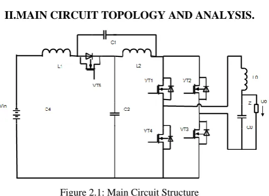
Figure 2.1: Main Circuit Structure
Fig.2.1 shows the circuit structure of the topology which based on quasi-Z-source network. It composes three parts: Input dc (battery, solar cell, and rectified dc), quasi Z source network and single phase Inverter Bridge.The structure of the Z-network is modified, compared to voltage fed Z-source inverter, that is, the position of the inductors, capacitors and the diode is different from that of voltage-fed Z-source inverter. This modification makes the average voltage of one of the quasi-Z-network capacitors decrease, and then, the cost, volume and weight of the wholesystem will also be decreased. Here the fully-controllable device V T5 is used in order to deal with the discontinuous operationcondition when the load is light, it is an IGBT module which composed of an IGBT andan anti-parallel diode to replace discrete components.The diode here is necessary in thequasi-Z-source inverter. This modification mainly aims to solve the light load abnormaloperation problem and when the load is normal, V T5 will not be turned on at all becauseits anti-parallel diode V D5 will keep on state during the non-shoot-through state.
The QZSI circuit differs from that of a conventional ZSI in the LC impedance networkinterface between the source and inverter. The unique LC and diode network connectedto the inverter bridge modify the operation of the circuit, allowing the shoot-throughstate which is forbidden in traditional VSI. This network will effectively protect the circuitfrom damage when the shoot through occurs and by using the shoot-through state, the(quasi-) Z-source network boosts the dc-link voltage. There are several differences betweenthe conventional and the current topology. The QZSI does not need a separateboost IGBT. The voltage boost is realized by switching a shoot through of the inverterduring zero state. Due to the higher boosting frequency the circuit devices L1, L2, C1,and C2 can be designed smaller accordingly, that is, the capacities are within a range of few Farads. In addition, the capacitors do not need to be electrolytic but can be film capacitors,whose life time is not dependent on ambient temperature. For regeneration the QZSI only needs one additional power electronic device, named VT5 when supply to load like electric vehicles engine. With the use of QZSI to supply the electric vehicle’s engine the electrolytic capacitor’s life time restrictions and the effort to control more additional power electronic devices do not apply, contrary to the conventional topology.
III.OPERATING PRINCIPLE
Active State
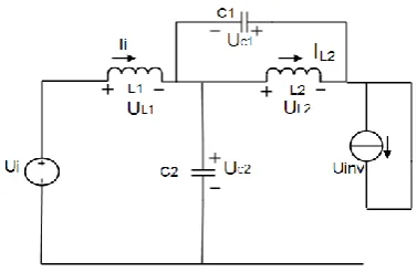
Figure 2.2: Equivalent Circuit for Active State
In the non-shoot through mode, in figure 2.2 the switching pattern for the QZSI is similar to thatof a VSI. The inverter bridge, viewed from the DC side is equivalent to a current source.The input dc voltage is available as DC link voltage input to the inverter, which makesthe QZSI behave similar to a VSI. The voltage across the load in this state is greater than zero.
Traditional Zero State
Figure 2.3: Equivalent Circuit for Zero State
In thestateshown in figure 2.3, the upper and lower two switches are turned on simultaneously and the powerdoes not flow to the load. In this case the output is an open circuit and it acts as zero valuecurrent source. Hence this traditional zero state can be integrated to the active state to forma Non shoot through state.
The third state shownin figure 2.4 the shoot through state is usually switched at the beginning and/or end of zero state when the voltage across the load is zero. In the shoot through mode, switches of the same phase VT1 and VT4 or VT2 and VT3in the inverter bridge are switched on simultaneously for a very short duration.The source however does not get short circuited when attempted to do so because ofthe presence LC network, while boosting the output voltage. The DC link voltage duringthe shoot through states, is boosted by a boost factor, whose value depends on the shootthrough duty ratio for a given modulation index.
Table2.1Analysis of voltages and currents
AS ZS ST
Load/Output v > 0, i ↑ v = 0, i ↓ v = 0, i ↓ L1, L2 v < 0, i↑ v < 0, i ↓ v > 0, i ↑ C1, C2 v↑, i> 0 v ↑, i> 0 v ↓, i< 0 Diode v = 0, i> 0 v = 0, i> 0 v < 0, i = 0
The table shows the theoretical analysis of voltages and currents and the behaviour of all quantities across inductance, capacitances and diode in all three possible states,(Active state, traditional zero state, Shoot through state) .The diode within the intermediate state can change the status during active state and zero state from conductive to blocking. This occurs if the diode current becomes less than or equal to zero.
IV. CIRCUIT ANALYSIS
Assuming that during one switching cycle Time T, the interval of the shootthrough stateis T0, the interval of non-shoot-through states is T1 thus T =T0 +T1 and the shoot-throughDuty ratio D
𝑇0/𝑇1 = 𝐷
During the interval of the non-shoot through stateT1 From Reference Figure 2.3
Ui = UL1 + UC2…….. (2.1)
UL2 = UC1 = UC2 – Uinv……….. (2.2)
During the interval of the shoot through state T0 From Reference figure 2.4
UL1 = Ui -UC1…………. (2.3)
UL2 = UC2; Uinv = 0………. (2.4)
The average voltage of the quasi-z-network inductors should be zero in a switching period From equations 2.1 to 2.4
𝑈𝐿2 =(𝑇1 ∗𝑈𝐶1) + (𝑇0 ∗ 𝑈𝐶2)𝑇 = 0……….. (2.5)
Or
𝑈𝐿2 =𝑇1 ∗ (𝑈𝐶2 − 𝑈𝑖𝑛𝑣 ) + 𝑇0 ∗(𝑈𝐶2)𝑇 =T……… (2.6)
𝑈𝐶1 𝑈𝐶2=
−𝑇0
𝑇1………. (2.7) 𝑈𝐶1
𝑈𝑖𝑛𝑣 = −𝑇1
𝑇 ………….. (2.8)
U0 = m * Uinv = B*m*Ui………… (2.9)
and therefore it is more reliablethan the traditional VSI. It is unnecessary to add a dead band into control schemes,which reduces the output distortion.
INVERTER SECTION
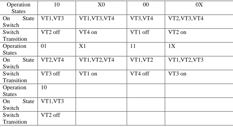
As the shoot-through zero state is inserted in the traditional zero state, thisnetwork will provideboost function to the novel Z-source or quasi-Z-source inverter, and will not lead to thedeterioration of the PWM control of the inverter.The insertions of shoot-through zerostate will increase the switching times of the power switches of the inverter bridge, and itwill increase the power loss of the switches. The switching orders can be reasonablyarrange to decrease the switching times. The operate state of a bridge leg is defined by threevalues 1, 0, and x, where 1 denotes the upper switch is on and the lower switch is off, 0denotes the upper switch is off and the lower switch is on, and x denotes both the upperswitch and the lower switch are on.
.
Table 3.1: Operating States and Switch Transition Operation
States
10 X0 00 0X On State
Switch
VT1,VT3 VT1,VT3,VT4 VT3,VT4 VT2,VT3,VT4 Switch
Transition
VT2 off VT4 on VT1 off VT2 on Operation
States
01 X1 11 1X On State
Switch
VT2,VT4 VT1,VT2,VT4 VT1,VT2 VT1,VT2,VT3 Switch
Transition
VT3 off VT1 on VT4 off VT3 on Operation
States
10 On State Switch
VT1,VT3 Switch
Transition
VT2 off
Therefore, the single-phase voltage fed quasi-Z-source inverter will have nine operating states, they are 10, 01, 00, 11, 0x, x0, x1, 1x, xx. If only singe inverter leg be shoot through is allowed, the xx state will be excluded. Then the switch order will be as 10 ,x0 , 00 , 0x , 01 , x1 , 11 , 1x , 10 as given in table . By choosing this order each state transition only need to turn on or turn off one switch, for example, 10 to x0 only need to turn on V T4 and then x0 to 00 only need to turn off V T1, etc. This will significantly decrease the switch times, so it increases the switching frequency and will not damage the power switches. The operation states and switch transition of the voltage-fed single phase quasi-Z-source inverter are shown in table 3.1.
V. CONTROL STRATEGY
The QZSI configuration has six active vectors when the DC voltage is impressed acrossthe load and two zero vectors when the load terminals are shorted through either loweror upper three switches. These total eight switching states and their combinations havebeen spawned many PWM control schemes. Sinusoidal PWM is the most commonlyused PWM technique in the VSI. On the other hand, QZSI has additional zero vectorsor shoot through switching states that are forbidden in traditional VSI. For an outputvoltage boost to be obtained, a shoot through state should always be followed by activestate. Three phase inverter must be controlled so that at no time both the switches in thesame leg are turned on or else the DC supply would be shorted. This requirement may bemet by the complimentary operations of the switches within a leg. There are three PWMstrategies
2. Maximum Boost control
3. Maximum constant boost control.
Simple boost control technique is used for this circuit
Simple boost control
The main idea of simple boost control method is using two DC voltage signals and twoAC voltage signals as modulation waves, compared with the high frequency carrier trianglewave, the value of the DC voltage could higher than or even equal to the peak valueof the AC voltages, then the control signals of the inverter bridge switches are obtained.To simplify the control circuit and decrease switch voltage stress, the DC voltage valueoften chosen should be equal to the peak value of the AC modulation wave; in this case,it is chosen that m + D = 1, and the shoot-through zero state duty cycle D is a constantvalue.Two straight lines are employed to realize the shoot through duty ratio. The upper one willbe the peak value of the sinusoidal wave. When the triangular carrier wave isgreater than the upper envelope Vp or lower than the lower envelope Vn the circuit turnsto the shoot through state , otherwise the circuit operates just as traditional carrier basedpwm.[9],[10]
VI. SIMULATION& RESULTS
Simulation Diagram
Simulation Results&Waveforms
To verify the analysis Simulation of QZSI is carried out for an input voltage of 24V ,Duty cycle of 0.3.For a switching frequency of 20kHz the components are chosen as C1=C2=1000µF,L1=L2=2mH,Connectedto a RL load .The simulation
Output Current Waveform &Output Voltage Waveform (Boost mode)
Output Current Waveform &Output Voltage Waveform (Buck mode)
Simulation Results
Modulation index
Output Voltage
Output Current
Capacitor Voltage C1
Capacitor Voltage C2 M=0.7
(Boost mode)
40V 1.75A 20V 50V
M=0.3 (Buck mode)
7V 0.3A 2V 22V
Applications of QZSI
Adjustable speed drives, motor drives
Grid connected photovoltaic systems
Uninterruptable power supply
Super capacitor energy storage
Electric vehiclesVII. CONCLUSION
application to ASD will show better results than VSI/CSI fed ASD. Output voltage canbe greater or smaller than input voltage. Thus, it is a verydesirable circuit topology when the input voltage range ofthe converter is wide.The operating principle of the proposed inverter was analysed in detail and simulation is carried out.
REFERENCES
[1] Xu Peng Fang, Xu Guang Wang, and Zhi Qiao Chen”A Single-Phase AC PowerSupply Based on Modified Quasi-Z-Source Inverter”IEEE Trans on AppliedSuperconductivity, VOL. 24, NO. 5, Oct 2014
[2] D. Cao, S. Jiang, X. H. Yu, and F. Z. Peng, “Low-cost semi-Z-source inverter forSingle-phase photovoltaic systems,” IEEE Trans. Power Electron, Dec. 2011.
[3] M. S. Shen et al.,”Constant boost control of the Z-source inverter to minimizeCurrent ripple and voltage stress,” IEEE Trans. Ind. Appl, vol. 42, no.3, May 2006.
[4]Muhammad H. Rashid, “Power Electronics Handbook”, by Academic Press 2001.
[5]B. K. Bose, Modern Power Electronics and AC Drives. Upper Saddle River, NJ: Prentice-Hall, 2002.
[6] M.Shen, J.Wang, A.Joseph, F.Z.Peng, L.M.Tolbert, and D.J. Adams, “Constant Boost Control of the Z-Source Inverter to Minimize Current Ripple and Voltage Stress”, IEEE Transaction on Industry Applications, vol. 42, No. 3, pp 770-778, May/June 2006.
[7] F. Z. Peng, “Z-source inverter,” in Conf. Rec. IEEE 37th IAS Annu. Meeting, Pittsburgh, PA, USA, Oct. 13–18, 2002, vol. 2, pp. 775–781. [8] P. C. Loh, D. M. Vilathgamuwa, Y. S. Lai, G. T. Chua, and Y. Li, “Pulse width modulation of Z-source inverters,” IEEE Trans. Power Electron., vol. 20, no. 6, pp. 1346–1355, Nov. 2005.
[9] P. C. Loh, D. M. Vilathgamuwa, C. J. Gajanayake, Y. R. Lim, and C. W. Teo, “Transient modelling and analysis of pulse-width modulated Z-source inverter,” IEEE Trans. Power Electron..