ISSN (Print) : 2320 – 3765 ISSN (Online): 2278 – 8875
I
nternational
J
ournal of
A
dvanced
R
esearch in
E
lectrical,
E
lectronics and
I
nstrumentation
E
ngineering
(An ISO 3297: 2007 Certified Organization)
Vol. 5, Issue 8, August 2016
Single or Multi Output High Efficiency
Flyback Converter
Muhammed Shefin1 , Geevarghese Mathew Kurian2
PG Student [PEPS], Dept. of EEE, KITS Engineering College, Kottayam, Kerala, India1
Head of the Department, Dept. of EEE, KITS Engineering College, Kottayam, Kerala, India2
ABSTRACT : Thesis work introduces an average current mode control of flyback rectifier with bidirectional switch. The proposed control scheme employs an outer voltage feedback loop, which maintains the output voltage as constant and an inner loop, which sense the input current. Average current mode control of flyback rectifier is suitable for obtaining a constant output with a varying input. Voltage equivalent of input current is averaged by using high gain current error amplifier, which again compared with the reference voltage. Reference voltage signal is produced by multiplying the rectified input voltage with the error output voltage. Gating pulse is generated by using this signal. Control method introduced in this work obtain better line and load regulation with the addition of inner current loop compared with voltage mode control. Also the rectified input voltage feedback achieves better input power factor. Conventional flyback rectifier is the inter connection of a diode bridge rectifier in the input side and a flyback converter. In order to obtain a highly efficient flyback rectifier with fewer losses an improved flyback rectifier is introduced. Here, two switches are connected in back to back to establish the bidirectional switch cell, which will conduct both in the positive and negative half cycle of the ac input voltage. The transformer with dual output windings with a diode in each winding reduces the current stress across each diode. New topology adds an extra switch in the primary side and a diode in the secondary side. This converter has the applications in battery charger. Improved bridgeless flyback rectifier only introduces a switch with common gate drive, a diode and an additional winding in the secondary side. Thus the weight of the converter is not affected with these additional components. Proposed average current mode control can be used as an adapter. Here also a multi output configuration of the proposed converter is modelled and also the MATLAB/SIMULINK models of the two topologies are implemented.
KEYWORDS : Multi output, Bidirectional Flyback Converter, MOSFET,Adapter ,Average current mode control
I.INTRODUCTION
DC-DC converters have been of great importance in power electronics because of its simple circuitry and efficient control schemes. With the help of this circuit output voltage can be varied steplesssly by controlling the duty ratio of the semiconductor device used in chopper. These converters find its application in SMPS, battery driven vehicles, electric traction, dc drives etc. DC-DC converters, also called as choppers are generally used for stepping up or down the DC supply. Conventional chopper circuits are buck, boost and buck boost. Among the various types of conventional DC-DC converters flyback converter has the added advantages such as simple structure with fewer components, isolation between input and output parts and is economic. Flyback converter is the most commonly used SMPS circuit which has the applications in low output power needs. In respect of energy conversion efficiency, flyback converter is inferior to many other SMPS circuits but it’s simple topology and low cost makes it popular in low output power range. Typical efficiency of flyback converter is around 65%-75%. Flyback converter can also operate over wide range of input voltage variation with single or multiple output windings. The primary and secondary windings of the flyback transformer don’t carry current simultaneously and in this sense flyback transformer works differently from a normal transformer.
ISSN (Print) : 2320 – 3765 ISSN (Online): 2278 – 8875
I
nternational
J
ournal of
A
dvanced
R
esearch in
E
lectrical,
E
lectronics and
I
nstrumentation
E
ngineering
(An ISO 3297: 2007 Certified Organization)
Vol. 5, Issue 8, August 2016
eliminating these diodes from the conduction path of the rectifier. Diodes are present in the primary side of the converter and various bridgeless topologies are introduced by eliminating the front end diodes.
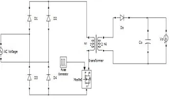
Flyback converter requires a single controllable switch like MOSFET and the usual switching frequency is in the range of 100 kHz. A two switch topology exits that offers better energy efficiency and less voltage stress across the switches. Input to the circuit may be unregulated DC voltage derived from the utility AC supply after rectification and some filtering. The ripple in DC voltage waveform is generally of low frequency and the overall ripple voltage waveform repeats at twice the AC mains frequency. Since SMPS circuit is operated at much higher frequency (in the range of 100 kW) the input voltage, in spite of being unregulated, may be considered to have a constant magnitude during any high frequency cycle. A fast switching devices like MOSFET is used with fast dynamic control over switch duty ratio to maintain the desired output voltage. The transformer in fig 1 used for voltage isolation as well as for better matching between input and output voltage and current requirements.
Fig. 1 Conventional flyback converter
Primary and secondary windings of the transformers are wound to have good coupling so that they are linked by nearly same magnetic flux. In fig 1, when Mosfet is on, the primary winding of the transformer gets connected to the input supply with its dotted end connected to the positive side.
At this time the diode Do connected in series with the secondary winding gets reverse biased due to the induced voltage in the secondary (dotted end potential being higher). Thus with the turning on of Mosfet, primary winding is able to carry current but current in the secondary winding is blocked due to the reverse biased diode. The flux established in the transformer core and linking the windings is entirely due to the primary winding current. This mode of circuit has been here as mode 1 circuit operation.
The mode-2 of circuit operation starts when the Mosfet is turned off for some time. The primary winding current path is broken and according to laws of magnetic induction, the voltage polarities across the windings reverse. Reversal of voltage polarities makes the diode in the secondary circuit forward biased. The stored energy is transferred to load as well output capacitor.
II. BIDIRECTIONALFLYBACKCONVERTER
ISSN (Print) : 2320 – 3765 ISSN (Online): 2278 – 8875
I
nternational
J
ournal of
A
dvanced
R
esearch in
E
lectrical,
E
lectronics and
I
nstrumentation
E
ngineering
(An ISO 3297: 2007 Certified Organization)
Vol. 5, Issue 8, August 2016
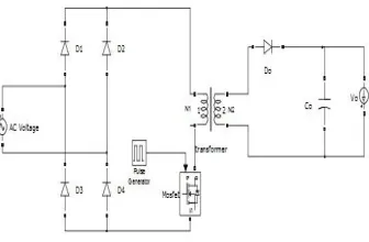
Fig. 2 Conventional flyback converter
compares the two circuits: the conventional flyback rectifier with the bridge diodes and the proposed bridgeless one. As shown in Fig. 3, the proposed rectifier eliminates the bridge diodes at the input side, in Fig. 2,and minimizes the conduction loss on the primary side. Considering that the general bridgeless rectifiers cannot remove all four bridge diodes for reverse voltage or current blocking and common mode noise reduction , the proposed circuit does not need any diode at all and further reduces the conduction loss. A few more circuit components are added to the proposed flyback rectifier as the tradeoff of eliminating four bridge diodes. However, the addition should be minimal because it generally increases the circuit complexity. Fig. 3 presents the proposed flyback rectifier: a switch on the primary side, M2, a diode on the secondary side, D0 , and the additional winding, N3, are newly added compared with the conventional circuit in Fig 2. These components give minimum effect to the circuit simplicity of the proposed circuit to secure the inherent advantage of the flyback converter, i.e, simple structure and low cost. M2 shares its source terminal and gate signal with S1 so that additional gate driver is not necessary. Adding D2 to the secondary side reduces the average current stress of both , D0 and D01 . Output diode current in the conventional rectifier, I Do in Fig. 2, is divided into I D0 and I D01 in the proposed rectifier in Fig. 3 according to the line voltage polarity. The divided output current makes the heat management of D0 and D01 easier than that of D0.
.
Fig . 3 Circuit Configuration Of Proposed Flyback Rectifier
ISSN (Print) : 2320 – 3765 ISSN (Online): 2278 – 8875
I
nternational
J
ournal of
A
dvanced
R
esearch in
E
lectrical,
E
lectronics and
I
nstrumentation
E
ngineering
(An ISO 3297: 2007 Certified Organization)
Vol. 5, Issue 8, August 2016
The proposed rectifier operates in constant-duty fixed frequency DCM controlled by a simple low-bandwidth voltage loop. The operation acquires high PF and low current distortion without any current control, because the average switch current is 12 per switching period is naturally proportional to the instantaneous line voltage Vin.
A. OPERATING PRINCIPLE
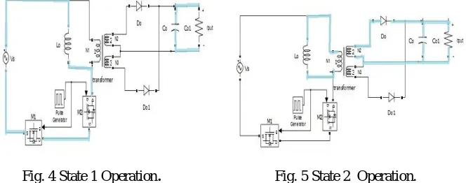
Assuming that the transformer has zero leakage inductance and the semiconductor devices have negligible on-state resistance and forward voltage drop, the proposed rectifier has four equivalent topological on-states in the steady-state operation according to the line voltage polarity and switching steady-state as shown in Fig.3. Lm and iLm are the transformer magnetizing inductance and its current respectively. The states are highly similar to the conventional flyback converter. States 1 to 2 from Fig. 4 to 5 occur when the line voltage vin is positive.N3 and D01 do not participate in the rectifier operation and does not conduct current.
1) During Positive Line Voltage
State I: State I occur at the positive start of line voltage Vin. Transformer output winding N3 and diode D01 do not participate in the rectifier operation and conduct no current. In state I, M1 and M2 turn ON and the positive Vin stores energy in L. iL and iS12 increase linearly and the output capacitor C0 supplies power to the load. A transformer design criterion should be met to avoid the unexpected turn-on of D01. Switch stress is equally shared by two switches M1 and M2. First three states, state I-III is for the positive input voltage and the other three states, state IV-VI is for the negative input voltage.
Fig. 4 State 1 Operation
.
Fig. 5 State 2 Operation.State II: Switches M1 and M2 will turn OFF at the beginning of state II. Thus the energy stored in the magnetizing inductance of the transformer is transferred to Co and load through N2 and D0. Magnetizing inductance current and switch current will start to decrease linearly. In state II also transformer tertiary winding and diode D01 is inactive
State III: State III starts when magnetizing current iL decreases and touches zero. At this mode parasitic capacitances of switches M1 and M2 resonate with L. Output current is always continuous and in this state output capacitor is supplying to the load.
ISSN (Print) : 2320 – 3765 ISSN (Online): 2278 – 8875
I
nternational
J
ournal of
A
dvanced
R
esearch in
E
lectrical,
E
lectronics and
I
nstrumentation
E
ngineering
(An ISO 3297: 2007 Certified Organization)
Vol. 5, Issue 8, August 2016
2) During Negative Line Voltage
States IV: State IV to VI occurs when input voltage Vin is negative. They are similar with the states I to III, except that iLm and Is01 have the opposite direction and N3 and D01 operate instead of N2 and D0.
State IV starts at the beginning of negative cycle of the input. Switches are triggered and magnetizing inductance of the transformer store energy. Switch current and magnetizing inductance current start to increase negatively
State V: In state V operation, two switches will be in the OFF state and the magnetizing inductor will discharge its energy to the load through transformer tertiary winding and D01. Upper windings of the transformer secondary and diode D0 is inactive during state IV-VI.
State VI: State VI will start when the energy stored in the inductor is completely discharged to the load. Again the parasitic capacitance of switches M1 and M2 resonate with the
magnetizing inductance of transformer. At this
state output capacitor C0 is supplying to the load
. If the proposed rectifier operates in a continuous conductionmode
Fig. 8 State 5 Operation. Fig. 9 State 6 Operation.
(CCM), states III and VI will not occur and states 1, 2, 4, and 5 will alternate according to the line voltage polarity. Key waveforms of the proposed rectifier as well as iS0 of the conventional rectifier are in Figure
III.CIRCUITDESIGN
A. DESIGN ANALYSIS
In bridgeless flyback rectifier, three main design analysis are considered. 1. Transformer turns ratio
2. 0utput capacitance.
3. Transformer magnetizing inductance
Three windings of the transformer are denoted as,N1,N2 and N3. N1 denotes the primary winding of the transformer. N2 andN33are the upper and lower windings of transformer secondary respectively. These secondary side windings has equal number of turns in order to make the voltage gain and frequency response as same for any input line voltage. Transformer turns ratio denoted as n, has the lowest limit as shown by the equation
n ≥ ,
ISSN (Print) : 2320 – 3765 ISSN (Online): 2278 – 8875
I
nternational
J
ournal of
A
dvanced
R
esearch in
E
lectrical,
E
lectronics and
I
nstrumentation
E
ngineering
(An ISO 3297: 2007 Certified Organization)
Vol. 5, Issue 8, August 2016
B. OUTPUT CAPACITANCE
The peculiarity of flyback rectifier is the absence of inductor in the circuit. Thus the design of flyback rectifier will be bit easier than other converter design. Because of the absence of the inductor in the output side, filtering action in flyback topology is done only by the output capacitor and the load resistor. One of the main drawbacks of flyback rectifier is that, the size of the capacitor will be larger in order to carry the full load current. In other converters, output current will share by the inductor and capacitor. Output capacitance can be calculated as,
Co =Dmax Po
f Vo ∆Vo D max = Maximum duty ratio
Po = output power f = switching frequency Vo =output voltage
C. TRANSFORMER MAGNETIZING INDUCTANCE
Important design criteria for selecting the magnetizing inductance of transformer is that, it should be smaller than a specified value in order to avoid unexpected operation of rectifier during continuous conduction mode. Magnetizing inductance of the transformer can be calculated based on the following equation,
L =(V −1)V . T D
2.5P . T
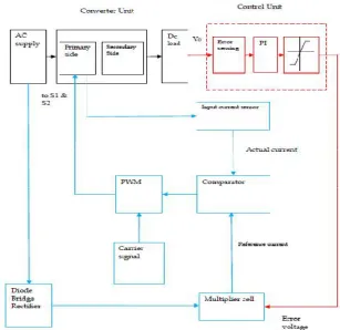
IV. AVERAGE CURRENT MODE CONTROL
The various modes of operation of the bridgeless flyback rectifier with bidirectional switch were described in the previous section. In order to operate satisfactorily in the various modes of the converter, a precise and well defined control method for flyback rectifier is explained in this section.
ISSN (Print) : 2320 – 3765 ISSN (Online): 2278 – 8875
I
nternational
J
ournal of
A
dvanced
R
esearch in
E
lectrical,
E
lectronics and
I
nstrumentation
E
ngineering
(An ISO 3297: 2007 Certified Organization)
Vol. 5, Issue 8, August 2016
Fig. 10 Average Current Mode Control Block Diagram Representation
V.SIMULATION
A. SIMULATION PARAMETERS
The simulations for flyback rectifier and bridgeless flyback rectifier is done in simulink/MATLAB.
TABLE 1
PARAMETERS USED IN SIMULATION
Output Capacitor 1.98mF
Output Voltage 48V
Switching Frequency 40kHz Magnetizing Inductance 370μH
Load Resistor 32Ω
The converter is fed from a 90-140(rms) V AC supply and the output of the converter is seen to be 48V DC.The power output of the converter is 72W.The results for simulaions are given in this chapter.
B. IMPROVED BRIDGELESS FLYBACK RECTIFIER
ISSN (Print) : 2320 – 3765 ISSN (Online): 2278 – 8875
I
nternational
J
ournal of
A
dvanced
R
esearch in
E
lectrical,
E
lectronics and
I
nstrumentation
E
ngineering
(An ISO 3297: 2007 Certified Organization)
Vol. 5, Issue 8, August 2016
Fig. 11 Simulink Model Of Bridgless Flyback Rectifier
C. SWITCHING CURRENT
Fig. 12 switching current
D. OUTPUT WAVEFORM
ISSN (Print) : 2320 – 3765 ISSN (Online): 2278 – 8875
I
nternational
J
ournal of
A
dvanced
R
esearch in
E
lectrical,
E
lectronics and
I
nstrumentation
E
ngineering
(An ISO 3297: 2007 Certified Organization)
Vol. 5, Issue 8, August 2016
E. AVERAGE CURRENT MODE CONTROL LED DESIGN
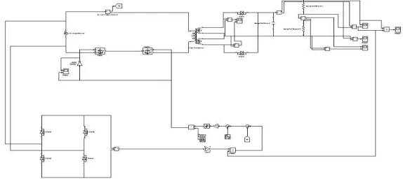
Fig. 14 Simulink Model Of Average Currewnt Mode Controlled Flyback Converter
F. OUTPUT WAVEFORM
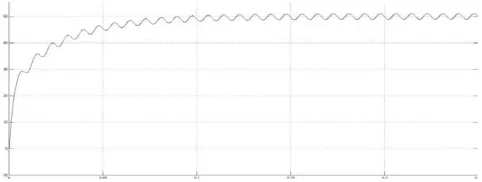
Fig. 15 Output Waveform Of Average Current Mode Controlled Flyback Converter
G. MULTI OUTPUT FLYBACK CONVERTER
ISSN (Print) : 2320 – 3765 ISSN (Online): 2278 – 8875
I
nternational
J
ournal of
A
dvanced
R
esearch in
E
lectrical,
E
lectronics and
I
nstrumentation
E
ngineering
(An ISO 3297: 2007 Certified Organization)
Vol. 5, Issue 8, August 2016
H. OUTPUTWAVEFORM
Fig. 17 Output Waveform Of Multi Output Flyback Converter
VI.CONCLUSIONANDFUTUREWORKS
A controlled bridgeless flyback rectifier for AC-DC conversion has been discussed. The rectifier is derived from the conventional flyback converter. Flyback converter can step up and step down the input voltage. MOSFETs are used as swtiching device in low power and high frequency switching applications. As the turn on and turn off time of MOSFETs are lower than other switching device, the switching losses are reduced.
Elimination of four diodes decreases the conduction loss, thus improves the efficiency of the converter. Transformer secondary is a dual output winding type and hence decreases the average current stress in the output diodes. Pulse width modulation control is used to control the flyback rectifier.
Replacement of RCD snubber with an efficient one will improves the efficiency of the converter . Also an average current mode control method will improve its efficiency and performance.
REFERENCES
[1]. Jong-Won Shin, Sung-Jin Choi ,”High-Efficiency Bridgeless Flyback Rectifier With Bidirectional Switch and Dual Output Windings”, Member, IEEE, IEEE TRANSACTIONS ON POWER ELECTRONICS, VOL. 29, NO. 9, SEPTEMBER 2014.
[2]. D. Tollik and A. Pietkiewicz, “Comparative analysis of 1-phase active power factor correction topologies,” in Proc. Int. Telecommunication Energy Conf., Oct. 1992, pp. 517–523.
[3]. A. F. Souza and I. Barbi, “High power factor rectifier with reduced conduction and commutation losses,” in Proc. Int. Telecommunication Energy Conf., Jun. 1999, pp. 8.1.1–8.1.5
[4]. J. C. Salmon, “Circuit topologies for PWM boost rectifiers operated from 1-phase and 3-phase ac supplies and using either single or split dc rail voltage outputs,” in Proc. IEEE Applied Power Electronics Conf., Mar. 1995, pp. 473–479.
[5]. Ismail EH. “Bridgeless SEPIC Rectifier With Unity Power Factor and Reduced Conduction Losses”, IEEE Transactions on Industrial Electronics; vol 56, no.4, pp.1147-1157, April 2009.
[6]. S.J. Chen and H. -C. Chang, “Analysis and implementation of low-side active clamp forward converters with synchronous rectification,” in Proc. 33rd Annu. Conf. Ind. Electron. Soc., 2007, pp. 1506–1511.