ISSN (Print) : 2320 – 3765 ISSN (Online): 2278 – 8875
I
nternational
J
ournal of
A
dvanced
R
esearch in
E
lectrical,
E
lectronics and
I
nstrumentation
E
ngineering
(An ISO 3297: 2007 Certified Organization) Vol. 4, Issue 9, September 2015
A Literature Review on Quantum Dots
Bal Krishan
1, Meenu Rani Garg
2Assistant professor, Dept. of ElectronicsEngineering , YMCAUST, Faridabad, , India1
PG Student [VLSI], Dept. of Electronics Engineering , YMCAUST, Faridabad, India2
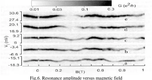
ABSTRACT: The paper aims to study physics of quantum dots. The review discusses the basic introduction of quantum dots(QDs) , QDs comparison with atoms, phenomenology of QDs , gate voltage characteristics , stability diagram of QDs , quantized charge tunnelling .The usage of QDs in practical applications in various fields has also been studied. Various present applications as well as the future scope of QDs have also been discussed .The paper also focuses on the study of various important parameters of QDs such as conductance versus gate voltage , resonance amplitude versus magnetic field.
KEYWORDS: Quantum Dots, QPCs , Conductance.
I. INTRODUCTION
The ongoing miniaturization of solid state devices often leads to the question: “How small can we make resistors, transistors, etc., without changing the way they work?” The question can be asked a different way, however: “How small do we have to make devices in order to get fundamentally new properties?” By “new properties” we particularly mean those that arise from quantum mechanics or the quantization of charge in units of e; effects that are only important in small systems such as atoms. “What kind of small electronic devices do we have in mind?” Any sort of clustering of atoms that can be connected to source and drain contacts and whose properties can be regulated with a gate electrode. Practically, the clustering of atoms may be a molecule, a small grain of metallic atoms, or an electronic device that is made with modern chip fabrication techniques. It turns out that such seemingly different structures have quite similar transport properties and that one can explain their physics within one relatively simple framework. In this paper we investigate the physics of quantum dots. Quantum dot is an artificially fabricated device. Typically, quantum dots are small regions defined in a semiconductor material with a size of order 100 nm . Since the first studies in the late eighties, the physics of quantum dots has been a very active and fruitful research topic. These dots have proven to be useful systems to study a wide range of physical phenomena. We discuss here in separate sections the physics of quantum dots. The name “dot” suggests an exceedingly small region of space.
II. LITERATURE SURVEY ON QUANTUM DOT
ISSN (Print) : 2320 – 3765 ISSN (Online): 2278 – 8875
I
nternational
J
ournal of
A
dvanced
R
esearch in
E
lectrical,
E
lectronics and
I
nstrumentation
E
ngineering
(An ISO 3297: 2007 Certified Organization) Vol. 4, Issue 9, September 2015
A. Comparison between Quantum dots and atoms
QDs often called the artificial atoms, however the QDs and atoms are compared in terms of various parameters.
Table-1 Comparing QDs with atoms
Parameter Atoms Quantum dots
Level spacing 1 eV 0.1 meV
Ionization energy 10 eV 0.1 meV
Typical magnetic field 104T 1-10 T
Size .1nm 100nm
In atoms the attractive forces are exerted by the nuclei , while in QDs –by background charges. The number of electrons in atoms can be tuned by ionization, while in QGs – by changing the confinement potential. This is similar by a replacement of nucleus by its neighbour in the periodic table.
III. PHENOMENOLOGY OF QDs
Figure 1 explains the phenomenology of QDs that how QDs are formed in Ga[Al]As heterostructure. In fig. 1 , the Au electrodes (bright) have a height of 100 nm. The two QPCs formed by the gate pairs F-Q1 and F-Q2 can be tuned into
the tunneling regime, such that a QD is formed between the barriers. Its electrostatic potential can be varied by changing the voltage applied to the center gate. Conductances of all QPCs can be tuned by proper gate voltages.The F-Q1 and F-Q2 pairs behave as perfect quantized QPCs. The contact F-C cannot be pinched off, but still shows depletion.
The central gate is designed to couple well to the dot, but with a weak influence on QPCs.
Fig.1 A QD in a Ga[Al]As heterostructure.
ISSN (Print) : 2320 – 3765 ISSN (Online): 2278 – 8875
I
nternational
J
ournal of
A
dvanced
R
esearch in
E
lectrical,
E
lectronics and
I
nstrumentation
E
ngineering
(An ISO 3297: 2007 Certified Organization) Vol. 4, Issue 9, September 2015
IV. GATE VOLTAGE CHARACTERISTICS
The gate voltage characteristic of QD is shown in fig. 2 .The conductance Vs gate voltage curve of fig. 2 shows pronounced oscillations in the curve . These oscillations may be because of coulomb blockade or because of resonant tunnelling.
Fig.2 Gate voltage curve showing pronounced oscillations. Fig.3 Variation of peak position versus magnetic field.
The position of 22 consecutive conductance resonances as function of the gate voltage and the magnetic field is shown in fig. 3 . The QD has an approximately triangular shape with a width and height of about 450 nm. The upper inset shows peak spacing at B=0 as a function of QD’s occupation.
The peaks are not equidistant because of the following reasons -
(1) There is a smooth dependence on the gate voltage, just because of change in the geometry (and consequently, in capacitances).
(2) In addition to a smooth dependence there are pronounced fluctuations – a rather rich fine structure.
ISSN (Print) : 2320 – 3765 ISSN (Online): 2278 – 8875
I
nternational
J
ournal of
A
dvanced
R
esearch in
E
lectrical,
E
lectronics and
I
nstrumentation
E
ngineering
(An ISO 3297: 2007 Certified Organization) Vol. 4, Issue 9, September 2015 One can discriminate between three main regimes:
(1) Weak magnetic fields-the spacing fluctuate , with a certain tendency to bunch together for small occupation numbers. (2) Intermediate regime-quasi periodic cusps(3) High magnetic fields.
V. STABILITY DIAGRAM FOR QD
QD is a zero-dimensional system, its density of states consists of a sequence of peaks, with positions determined by size and shape of the confining potential, as well as by effective mass of the host material. The stability diagram for quantum dot is shown in fig. 5.
Fig. 5(a) ,(b) Stability Diagram for QD.
The stability diagram for QD resembles diamond structure for Coulomb blockage (SET) system. However, size of diamonds fluctuates. At low bias – it resembles usual CB oscillations. At larger bias a fine structure emerges , which is absent in SETs.
Fig.6. Resonance amplitude versus magnetic field
ISSN (Print) : 2320 – 3765 ISSN (Online): 2278 – 8875
I
nternational
J
ournal of
A
dvanced
R
esearch in
E
lectrical,
E
lectronics and
I
nstrumentation
E
ngineering
(An ISO 3297: 2007 Certified Organization) Vol. 4, Issue 9, September 2015 .
VI. QUANTIZED CHARGE TUNNELING
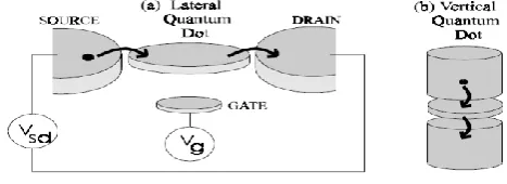
Quantized charge tunnelling phenomenon examines the circumstances under which Coulomb charging effects are important. In other words, we answer the question, “How small and how cold should a conductor be so that adding or subtracting a single electron has a measurable effect?” To answer this question, let us consider the electronic properties of the small conductor depicted inFig.7, which is coupled to three terminals. Particle exchange can occur with only two of the terminals, as indicated by the arrows. These source and drain terminals connect the small conductor to macroscopic current and voltage meters. The third terminal provides an electrostatic or capacitive coupling and can be used as a gate electrode. If we first assume that there is no coupling to the source and drain contacts, then our small conductor acts as an island for electrons.
Fig. 7 Schematic of a quantum dot, in the shape of a disk, connected to source and drain contacts by tunnel junctions and to a gate by a capacitor. (a) shows the lateral geometry and (b) the vertical geometry.
The number of electrons on this island is an integer N, i.e. the charge on the island is quantized and equal to Ne. If we now allow tunnelling to the source and drain electrodes, then the number of electrons N adjusts itself until the energy of the whole circuit is minimized. When tunneling occurs, the charge on the island suddenly changes by the quantized amount e. The associated change in the Coulomb energy is conveniently expressed in terms of the capacitance C of the island. An extra charge e changes the electrostatic potential by the charging energy EC= e2/C. This charging energy
becomes important when it exceeds the thermal energy kBT. A second requirement is that the barriers are sufficiently
opaque such that the electrons are located either in the source, in the drain, or on the island. This means that quantum fluctuations in the number N due to tunnelling through the barriers is much less than one over the time scale of the measurement. (This time scale is roughly the electron charge divided by the current.) This requirement translates to a lower bound for the tunnel resistances Rt of the barriers. To see this, consider the typical time to charge or discharge the
island ∆t = RtC. The Heisenberg uncertainty relation: ∆E∆t = (e2/C)RtC>h implies that Rt should be much larger than
the resistance quantum h/e2= 25.813 KΩ in order for the energy uncertainty to be much smaller than the charging
energy. To summarize, the two conditions for observing effects due to the discrete nature of charge are
Rt >> h/e2
e2/C >> kBT
The first criterion can be met by weakly coupling the dot to the source and drain leads. The second criterion can be met by making the dot small.
VII. USAGE AND APPLICATIONS OF QDs
ISSN (Print) : 2320 – 3765 ISSN (Online): 2278 – 8875
I
nternational
J
ournal of
A
dvanced
R
esearch in
E
lectrical,
E
lectronics and
I
nstrumentation
E
ngineering
(An ISO 3297: 2007 Certified Organization) Vol. 4, Issue 9, September 2015
phosphor integration by dot’s ability to absorb and emit at any desired wavelength. Utilizing QDs in solar cells allow realization of 3rd generation solar cells at approximately 60% efficiency in electricity production . Solar cells utilizing QDs are effective due to QDs ability to preferentially absorb and emit radiation that results in optimal generation of electric current and voltage. QDs also have future applications. They can be used in defence applications. Integrate QDs into dust that tracks enemies. QDs also provide protection against friendly-fire events. QDs also have the ability to specifically control absorption and emission spectra to produce unique validation signatures.
VIII. CONCLUSION
Quantum dots are really just a generic example of a small, confined structure containing electrons. There is no fundamental physical discontinuity between a quantum dot and a large molecule or even an atom. There should be no surprise then, that the physics of dots applies as well to small metallic particles, clusters, and molecules. Carbon nanotubes, the extended cousins of C60, have also proven to be a system that can be understood using the ideas
developed for dots . The nanotube is predicted to act as a one-dimensional quantum wire, and a finite length turns it into a one-dimensional quantum dot. QDs have been found useful due to their sensing capability for various particular applications, in fields such as optoelectronics and medicine. The main reasons for their use for medical purposes are the following: excitation wavelength far from the emission, inherent photo stability and long fluorescent life time.
REFERENCES
[1] M. Reed, Scientific American 268, 118 (1993). [2] M. Kastner, Physics Today 46, 24 (1993).
[3] Single Charge Tunneling, edited by H. Grabert and M.H. Devoret (Plenum Press, 1991).
[4] D.V. Averin and K.K. Likharev, J. Low Temp. Phys. 62, 345, (1986); and in: Mesoscopic Phenomena in Solids, edited by B.L. Altshuler, P.A. Lee, and R.A. Webb (Elsevier,1991).
[5] G. Schön and A.D. Zaikin, Physics Reports 198, 237 (1990); G.-L. Ingold and Yu. V. Nazarov, in Ref. 3; R. Fazio and G. Schön, in this volume. [6] Kluson, P.; Drobek, M.; Bartkova, H.; Budil, I. Welcome in the Nanoworld. Chem. Listy 2007, 101, 262-272
[7] H. van Houten, C.W.J. Beenakker, A.A.M. Staring, in Ref. 3. [8] U. Meirav and E.B. Foxman, Semicond. Sci. Technol. 10, 255 (1995).
[9] L.P. Kouwenhoven and P.L. McEuen, in Nano-Science and Technology, edited by G. Timp (AIP Press, 1997). [10] Special issue on Single Charge Tunneling, edited by H. Grabert, in Zeitschrift für Physik B 85(1991).
[11] Special issue on Few-Electron Nanostructures, edited by L.J. Geerligs, C.J.P.M. Harmans, and L.P. Kouwenhoven, in Physica B 189(1993). [12] C.J.P.M. Harmans, Physics World 5, 50 (1992).
![Figure 1 explains the phenomenology of QDs that how QDs are formed in Ga[Al]As heterostructure](https://thumb-us.123doks.com/thumbv2/123dok_us/7784730.1287392/2.595.153.447.531.728/figure-explains-phenomenology-qds-qds-formed-ga-heterostructure.webp)