Implementation of Universal filter using DVCC on
120nm Technology
Chetna Dhanariya
#1, Mohd. Abuzer Khan
*2 #Electronics & Communication, R.G.P.V Bhopal L.K.C.T. Indore M.P. India
1
Abstract:- In this paper we are focus on CMOS high performance, high bandwidth and high frequency current mode signal DVCC-II is presented and provides high driving capability. We use DVCC-II for implementation of single input and multiple output, multiple input and single output filter. In DVCC-II block three stages connected in circuit and rail to rail input-output operation. The proposed second generation DVCC has been designed in 0.12µm CMOS technology with 1.5V supply voltage. Tanner tool simulator is used for circuit simulation. In low voltage sub-micrometer analog circuit accuracy and precision can be limited by the finite gain as well as by input offset voltage. Proposed circuit features have high gain, high bandwidth and low power dissipation that can be achieved simultaneously without requiring well matched register.
Keywords: - Second generation current conveyor circuit, class AB amplifier, trans-conductance, tanner tool.
I.
INTRODUCTION
Voltage based circuits depends on the voltage-feedback amplifier (voltage operational amplifier) have disadvantage of severe reduce bandwidth at higher gains, because of operational amplifier’s fixed gain/bandwidth product. An attempt to overcome this problem, current conveyor is proposed by Sedra have been acknowledged to be versatile building blocks for current mode signal processing. The first current conveyor (CC-I) was introduced in 1968 and are rarely available.
Figure 1 current conveyor
The original current conveyor is shown in figure 1. It is a three terminal device (two input terminals X and Y and one output terminal Z).
The remaining paper is organized as follows. In next section the proposed DVCC-II CMOS circuit realization and filter design. Section III introduces simulation results.
II. DVCC CIRCUIT REALIZATION
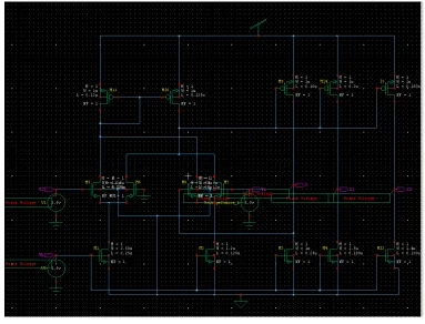
Figure 2 Schematic view of DVCCII
All transistors are assumed to be operating in saturation. The operation of a wide linear range trans-conductor relies mainly on biasing along tail differential pair LTDP (M1–M2) with a dynamic tail current Iss that increases with V2id where
Vid= VY1 - VY2
Since the output current produced at the drains of M2 and M6 is expressed by
A) Proposed Multiple inputs Single
Output:-In this section the proposed DVCC is used to realize a MISO second-order LP-BP filter as shown in the figure 3.Two different responses are achieved depending on the actual active input. If the first input is active, while the second one is grounded, an inverting band-pass response is obtained. On the other hand, grounding the first input while activating the second one generates a non-inverting low-pass response.
Figure 3 Multiple input Single Output filter
Figure 4 Single Input Multiple Outputs Filter
III. SIMULATION RESULTS
Simulation Results For
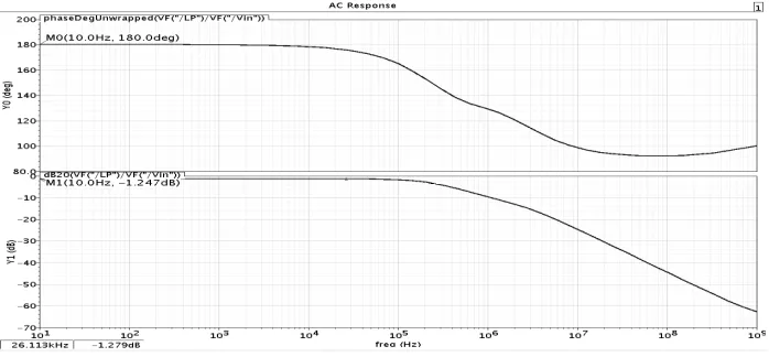
DVCC-II:-Figure 5 Magnitude and Phase Response of DVCC-II
Figure 6 Response of Low-Pass Filter
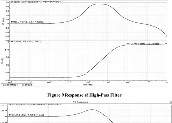
Figure 7 Magnitude Response of High-Pass Filter
Figure 9 Response of High-Pass Filter
Figure 10 Magnitude Response of Band-Pass Filter
IV. REFERENCE
[1] Google Wikipedia
[2] Sedra A, Smith K. A second-generation current conveyor and its applications. IEEE Transactions on Circuit Theory 1970; 17:132–4.
[3] SEDRA, A.S, ROBERTS, Gw., and GOHH, F: ‘the
current conveyor: History, progress and new results’,
IEE Proc. G, Circuits Devices Syst., 1990, 137, (2), pp. 78-87.
[4] Mahmoud SA. Fully differential CMOS CCII based on
differential difference trans-conductor. Analog
Integrated Circuits and Signal Processing 2007; 50:195–203.
[5] Ismail AM, Soliman AM. Novel CMOS liberalized balanced output trans-conductance amplifier based on differential pairs. Frequenz 1999;53:170–4
[6] Mahmoud SA. Fully differential CMOS CCII based on
differential difference trans-conductor. Analog
Integrated Circuits and Signal Processing 2006; 49:267–79.
SINENCIO, E.: 'Low-voltage class AB buffers with
quiescent current control', IEEE J. Solid- State
Circuits, 1998, 33, (6), pp. 915-919.
[8] FABRE, A, SAAID, O., WIEST. F. and
BOUCHERON, C.: ‘High frequency application based
on a new current controlled conveyor’, IEEE Trans.
Circuits Syst.-I, 1996, CAS-43, (2), pp. 82-91. [9] W.Chiu, S. I. Liu, H. W. Tsao, and J. J. Chen, “CMOS
differential difference current conveyor and their application” IEE Proc. Circuit Device Syst, Vol. 143(2), pp.91-96, 1996.
[10] U. KUMAR, “Current Conveyor: A review of state of the art, “IEEE Circuit & syst, Mag., vol. 3, pp 10-13.1981 [11] B. Wilson, “Recent developments in current
conveyors and current mode circuits,” IEE Proc., vol. 137,Pt. G ,pp 63-77,1990.