Abstract
SAYED, ISLAM ESMAT MOHAMED MOHAMED HASHEM SAYED. Quantum Wells to Improve the Performance of III/V Multi-junction Solar Cells. (Under the direction of Dr. Salah M. Bedair.)
The current state of the art solar cells based on four-junction III/V materials have realized efficiencies of ~46% under high solar concentration. Multiple studies have reported that improving the efficiency of solar cells to higher than 50% will reduce the cost of solar ($/watt) and might open new opportunities in the solar photovoltaic concentrator market. In this dissertation, we aim to develop a new approach to enhance the efficiency and reduce the cost of solar ($/watt) through providing new materials and device architectures that can be part of next-generation photovoltaic devices with target efficiencies higher than 50%.
This dissertation demonstrates two novel quantum well structures that can be part of next-generation five (or more) junction devices with a prospective efficiency higher than 50% under high solar concentration. The first quantum well structure is strain-balanced InGaAsP/InGaP quantum wells, where the InGaAsP quantum well is grown under compressive stress and the InGaP barrier is grown under tensile stress. The second quantum well structure is lattice-matched InGaAsP/InGaP, where InGaAsP and InGaP layers have lattice constants similar to the underlying substrate. In both structures, the quantum wells are included in the unintentionally doped region of In0.49Ga0.51P p-i-n on GaAs substrates. The two quantum well structures are characterized and analyzed by optical microscopy, X-ray diffraction,
photoluminescence, current-voltage characteristics, and external quantum efficiency.
transport for both electrons and holes. The short circuit current density of the lattice-matched InGaAsP/InGaP quantum well solar cell is 26% higher than that of a standard InGaP cell that does not include quantum wells.
© Copyright 2018 by Islam Esmat Mohamed Mohamed Hashem Sayed
Quantum Wells to Improve the Performance of III/V Multi-junction Solar Cells
by
Islam Esmat Mohamed Mohamed Hashem Sayed
A dissertation submitted to the Graduate Faculty of North Carolina State University
in partial fulfillment of the requirements for the degree of
Doctor of Philosophy
Electrical Engineering
Raleigh, North Carolina
2018
APPROVED BY:
_______________________________ _______________________________
Salah M. Bedair Robert Kolbas
Chair of Advisory Committee
_______________________________ _______________________________ Mehmet Ozturk Nadia El-Masry
ii
Dedication
To my parents: Samia Azzazi and Esmat Hashem,
iii
Biography
I was born in Cairo, Egypt on October 4th, 1988. My father, Esmat, is a mechanical engineer and former Colonel in the Egyptian Army, and my mother, Samia, is an accountant manager. My love for mathematics and physics has driven me to join the faculty of engineering at Cairo University. In 2010, I received the B.Sc. (Hons.) in Electronics and Electrical Communications Engineering. In the same year, I joined the staff at the Department of Engineering Physics, Cairo University, as a teaching and research assistant. From 2011 to 2013, I was research assistant at The Youssef Jameel Center for Science and Technology, The American University in Cairo. My masters research project was about developing nano-rectennas for infrared energy harvesting.
Under the direction of Prof. S. M. Bedair, I started my Ph.D. journey at North Carolina State University in 2013. During my Ph.D., I interned with the III/V group at the National Renewable Energy Laboratory. My Ph.D. research investigated new materials and device architectures for next-generation photovoltaic devices. During my MSc and Ph.D. graduate career, I have authored or co-authored more than 15 publications in the field of renewable energies. I received first place award at the 2016 NCSU ECE GSA research symposium, first place award at the 2017 State Energy Conference of North Carolina, overall grand prize award at the 5th annual North Carolina MRS Triangle Student Research Competition, third place award at the 2017 NCSU ECE GSA research symposium, and second place-best oral presenter award at the Carolina Science Symposium. I was a finalist at the 2017 Three Minute Thesis Competition organized by NCSU Graduate School and a finalist in best student paper award competition at the 44th IEEE Photovoltaic Specialist Conference (PVSC). In 2017, I was named Preparing the Professoriate Fellow by NCSU Graduate School.
iv
Acknowledgments
I am indebted to my Ph.D. advisor, Dr. S. M. Bedair, for giving me an invaluable opportunity to work under his supervision at NCSU. I value all what Dr. Bedair has taught me through our discussions about my research and life as a scientist. Thank you for helping me grow into the researcher that I am today. There is no doubt that Dr. Bedair’s exceptional love for science has a great impact on my graduate career and that my life would be very different today if I did not work under his supervision.
I would like to thank my advisory committee, Dr. Mehmet Öztürk, Dr. Robert Kolbas, and Dr. Nadia El-Masry. I have a great respect for their research, and I am thankful that they agreed to serve on my committee.
I would like to thank the current and former members of the Bedair group who helped me immensely to progress with my research. I would like to thank Zachary Carlin for mentoring me at the beginning of my research career at NCSU. I thank Zach for many useful discussions that enriched our research and for being my friend. I would like to thank Peter Colter for all the “sciency” conversations that I will certainly miss. Peter is one of the most knowledgeable people that I have worked with and he helped me considerably as I progressed with my research. Thanks to Brandon Hagar for his valuable input on my project. Thanks to Brent Allen for helping me progress faster in the MOCVD lab during my first few weeks. I would like to thank current and former members of the LED group, Dennis Van Den Broeck, Deon Bharrat, William Campbell, and Judi Reynolds, for many useful discussions. I would like also to thank Mostafa Abdelhamid whose exceptional personality made my life inside and outside the lab more fun.
v
discussions. I would like to thank Waldo Olavarria for the MOVPE growth of my QW samples and Michelle Young for processing my devices. I would like to thank Nasser Karam for facilitating this opportunity for me.
This research was supported by the National Science Foundation: Goali 1102060 and 1407772. The research conducted at NREL was supported by the U.S. Department of Energy under contract no. DE-AC36-08GO28308.
I would like to thank my friends in Raleigh who were my family while I am thousand miles away from Egypt.
A few weeks before the completion of this research, a great and very humble person has left our world with a pleasant smile on his face, my uncle Abdelaziz. I love you and will always miss you.
Finally, I would like to thank my parents, Samia Azzazi and Esmat Hashem, for their unconditional love, daily encouragement, and for having my education as a top priority in their life. I would like to thank my sister Marwa and my brother Amr for their love and support.
vi
Table of Contents
List of Tables ... ix
List of Figures ... x
Chapter 1: Introduction ... 1
1.1. P-N Junction ... 2
1.2. P-N Junction under Illumination ... 7
1.3. Losses in Single-junction Solar Cells ... 11
1.4. Multi-junction Solar Cells ... 14
1.5. Research Objectives ... 17
1.6. Synopsis of Dissertation ... 19
Chapter 2: Principles of Quantum Well Solar Cells... 21
2.1. Motivation ... 21
2.2. Quantum Well Solar Cells (Review) ... 22
2.2.1. Quantum Well Material Systems ... 24
2.2.2. Advantages of Quantum Well Solar Cells ... 25
2.3. Bandgap Tunability ... 27
2.4. Critical Layer Thickness Constraints ... 29
2.5. Strain Balance Design and Criteria ... 31
2.6. Carrier Transport ... 33
Chapter 3: Review of Recent Progress in Quantum Well Solar Cells ... 37
3.1. Strain-balanced InGaAs/GaAsP Quantum Wells ( 1.1-1.3 eV Subcell) ... 37
3.2. Strained InGaN/GaN Quantum Wells ( > 2.1 eV subcell) ... 42
Chapter 4: Growth and Characterization of Strain-Balanced InGaP-based Quantum Wells ... 48
4.1. Motivation ... 48
4.2. Potential Solar Cells with Bandgaps in the 1.6-1.8 eV range ... 49
4.3. Experimental Approaches ... 52
4.3.1. Growth details... 53
4.3.2. Fabrication Details ... 55
vii
4.4. Results and Discussion ... 56
4.4.1. Well and Barrier Calibrations ... 56
4.4.2. Critical Layer Thickness Constraints ... 58
4.4.3. Zero-stress Balance Model and X-ray Diffraction ... 59
4.4.4. Optical Microscopy ... 61
4.4.5. Photoluminescence Results of InGaAsP/InGaP and InGaP/InGaP SBMQWs (emission and modeling) ... 61
4.4.6. Quantum Efficiency and Light Current-voltage Characteristics ... 64
Chapter 5: Strain-balanced InGaAsP/ InGaP Quantum Well Solar Cells ... 67
5.1. Introduction ... 67
5.2. Experimental Details ... 68
5.3. Results and Discussion ... 69
5.3.1. Photoluminescence and Electroluminescence of SBMQWs: red-shift ... 70
5.3.2. X-ray Diffraction ... 72
5.3.3. Carrier Transport and Well Thickness Effect ... 73
5.3.4. Quantum Efficiency and Current Voltage Characteristics (well thickness effects) ... 74
5.3.5. Quantum Efficiency: Measurements and Modeling ... 79
5.3.6. Effect of Number of Period on InGaAsP/InGaP SBMQWs ... 80
5.4. Advantages and Limitations of Strain-balanced InGaAsP/InGaP Quantum Well Solar Cells ... 85
Chapter 6: Growth and Characterization of Lattice-matched InGaAsP/InGaP Quantum Wells... 87
6.1. Introduction ... 87
6.2. Experimental Details ... 89
6.3. Results and Discussion ... 91
6.3.1. Effect of Arsenic to Phosphorus Ratio in InGaAsP on Stress and XRD Peaks Sharpness ... 91
6.3.2. Effect of Substrate Miscut ... 95
6.3.3. Effect of Growth Interruptions ... 98
viii
Chapter 7: Lattice-matched InGaAsP/ InGaP Quantum Well Solar Cells ... 102
7.1. Introduction ... 102
7.2. Experimental Details ... 104
7.3. Results and Discussion ... 104
Chapter 8: Photon recycling in multi-junction solar cells using the Inter-Metallic Bonding Approach: Concept ... 114
8.1. Motivation ... 114
8.2. Current status of photon recycling and light trapping in “single-junction” cells ... 116
8.3. Current status and approaches of photon recycling in “MJ solar cells” and limitations (Review) ... 118
8.3.1. Use of Distributed Bragg Reflectors (DBRs) ... 118
8.3.2. Use of buried Al2O3 through lateral oxidation of AlAs [172] ... 118
8.3.3. Use of n = 1.5 epoxy as a reflector and ZnS as an antireflection coating [173] . 119 8.3.4. Use of photoresist to print one cell on another ... 120
8.4. Photon recycling in 2J tandem cells by an Intermetallic Bonding (IMB) approach .. 120
8.5. Analysis of photon recycling in dual-junction solar cell structures: Open circuit voltage and external Luminescence efficiency ... 122
8.6. Analysis of photon recycling in dual-junction solar cell structures: Air gap effects . 125 8.6.1. Modeling the front and back reflectance across multiple layers ... 125
8.6.2. Front and back reflectance results ... 127
Chapter 9: Summary and Future Outlook ... 130
9.1. Summary of Research ... 130
9.2. Challenges and Future Outlook ... 132
9.2.1 Stress management issue ... 134
9.2.2 Carrier transport issue ... 134
9.2.3 Electric field and background doping issue ... 134
ix
List of Tables
Table 3.1: Tunneling (Ptun) and thermionic-emission (Ptherm) escape probabilities for
electrons and heavy hole states for different InGaAs/GaAsP QW designs ... 39
Table 5.1: Thickness of well and barrier, peak PL emission, short circuit current density, open circuit voltage, bandgap-voltage offset (Woc) , FF and efficiency (η) for standard cell and SBMQW cells. The devices did not contain antireflection
coatings or a window. ... 74
Table 5.2: Number of periods, grown MQW layer thickness, short circuit current density, open circuit voltage, and fill factor for series of InGaAsP/InGaP SBMQW cells. The devices did not contain antireflection coatings or
windows. ... 81
Table 7.1: One-sun AM1.5 short circuit current contribution of the QWs (∆Jsc¸), effective
junction bandgap (Eg), open circuit voltage (Voc), and bandgap-voltage offset
(Woc) for the studied samples. ... 106
Table 7.2: Tunneling escape and thermionic emission escape probabilities for electrons and heavy hole states ... 112
x
List of Figures
Figure 1.1: (a) schematic of p-n junction, (b) doping concentration profile of InGaP p-n junction. ... 2
Figure 1.2: Schematics of In0.49Ga0.51P p-n junction at thermal equilibrium (zero-bias/without illumination): (a) Energy band diagram, showing the drift and diffusion carriers’ components. The horizontal black dotted line is the Fermi level, (b) charge density within space charge region, (c) electric field
distribution, and (d) electrostatic potential. Simulations were performed using PC1D. ... 3
Figure 1.3: (a) Band profiles and (b) carrier densities for an In0.49Ga0.51P p-n junction at zero bias (blue) and forward bias (red). (c) Band profiles and (d) carrier densities for an In0.49Ga0.51P p-n junction at zero bias (blue)and reverse bias (red). The arrows in Figures (a) and (c) show the direction of the electron and hole transport following forward and reverse bias. ... 5
Figure 1.4: Measured dark current-voltage characteristics of InGaP p/n junction, grown and processed at NCSU. ... 6
Figure 1.5: The solar spectrum irradiance, AM0, AM1.5G, and AM1.5D ... 7
Figure 1.6: (a) Illuminated P-N junction, (b) energy band diagram and (c) carrier densities for illuminated InGaP p-n junction. The arrows in Figure (b) show the direction of the electron and hole transport following photo-generation. ... 8
Figure 1.7: Measured dark and illuminated current-voltage characteristics of In0.49Ga0.51P p-n junction. The figure also shows the metrics that are used to assess the
solar cell performance, Voc, Jsc, and maximum power point. ... 10
Figure 1.8: Energy band diagram of a PN junction with incident photons of energies higher than, equal to, or less than the bandgap, showing both the
thermalization and sub-bandgap losses that exist in single-junction solar cells. ... 12
Figure 1.9: Schematics of AM1.5 spectrum showing the thermalization and
sub-bandgap losses for single junction solar cells: (a) silicon, with an Eg of 1.1 eV,
(b) subcell, with an Eg of 1.70 eV. ... 13
xi
included. The efficiency will be more reduced if radiative-recombination and SRH recombination losses are included. These calculations were performed on the AM1.5G spectrum ... 14
Figure 1.11: Multi-junction solar cell concept ... 15
Figure 1.12: Schematics of AM1.5 spectrum showing the thermalization and sub-bandgap losses for multi-junction solar cell devices: (a) dual-junction
structure (1.7eV/1.1 eV), (b) six-junction structure (2.1 eV/1.7 eV/1.4 eV/1.1 eV/0.91 eV/0.7 eV). ... 15
Figure 1.13: Cumulative loss from carrier thermalization to the band edges of single-junction 1.1 eV, three-single-junction (1.87/1.4/0.7 eV), and six-single-junction (2.1 eV/1.7 eV/1.4 eV/1.1 eV/0.91 eV/0.7 eV) devices. The integrated power density of AM1.5G is 1000 watt/m2 ... 16
Figure 1.14: Quantum well solar cells ... 17
Figure 1.15: Schematic of photon dynamic in multi-junction cells with an ideal reflector placed at the back of the top cell. Antireflection coatings (ARCs) are not shown for simplicity. This will be experimentally realized using the using the Inter-Metallic Bonding (IMB) Approach [28] ... 19
Figure 2.1: Schematics of: (a) GaAs p-i-n solar cell that includes strain-balanced InGaAs/GaAsP quantum wells, grown on GaAs substrate, and (b) GaN p-i-n solar cell that includes strained InGaN/GaN quantum wells, grown on GaN
templates on sapphire substrate. ... 23
Figure 2.2: Bandgap versus lattice constants showing the well and barrier compositions for the three QW structures in Figure 1: (a) strain-balanced InGaAs/GaAsP QWs, and (b) strained InGaN/GaN QWs. The vertical dotted line in each figure represents the lattice-matched condition to GaAs/GaN. The horizontal dotted lines represent the region of interest in each QW structure. ... 24
Figure 2.3: Effective bandgap versus well thickness (tw) for various indium compositions in wells for the following structures: (a) strain-balanced InGaAs/GaAs0.35P0.65, and (b) strained InGaN/GaN. The barrier thickness (tb) of GaAs0.35P0.65 was adjusted to achieve the strain-balance condition. The GaN barrier thickness
was fixed at 80 Å... 29
Figure 2.4: Critical layer thickness versus the indium content for: (a) InxGa1-xAs well,
xii
Figure 2.5: Thickness of wells and barriers as estimated by zero-stress balance model to strain-balance the following two structures to GaAs substrates:
InGaAs/GaAs0.35P0.65 with various indium% in InGaAs well. The CLT of each well composition is added to the figure. ... 32
Figure 2.6: Band diagram of quantum well solar cells with two different designs: (a) structure with thin wells and low effective barrier height to promote thermionic emission, and (b) structure with thin barriers to allow carrier tunneling. In both scenarios, the carriers are swept across the depletion region by an electric field. ... 34
Figure 3.1: External quantum efficiency of multiple InGaAs/GaAsP quantum well solar cells designs: (a) structure with thin wells and low effective barrier height to promote thermionic emission, by Adams et al. [69], (b) structure with thin barriers to allow carrier tunneling, by Bradshaw et al.[41, 70], and (c) high-performance structure with peak excitonic values exceeding 70%, by Fuji et al. [40]. More details about these structures such as the presence of window, back surface field or antireflection coatings are discussed in the references. ... 38
Figure 3.2: AM1.5 current-voltage characteristics of InGaAs/GaAsP QW and GaAs standard solar cells, with the inset showing a schematic of the two structures, by Fuji et al. [40]. ... 41
Figure 3.3: The effect of the number of QWs in the intrinsic region on one-sun AM0 current-voltage characteristics: (a) Jsc (mA/cm2) and Voc (Volts) and (b) FF
and η; study by Bushnell et al. [78]... 42
Figure 3.4: External quantum efficiency of InGaN/GaN QW solar cells with high
indium percentage (x > 0.2): (a) eight periods of In0.30Ga0.70N (tw = 30 Å)/GaN (tb = 80Å) that has a cut-off wavelength at ~450 nm, by Dahal et al. [43] and (b) 30-period In0.28Ga0.72N (tw = 22 Å)/GaN (tb = 80Å) that has a cut-off wavelength at ~500 nm by Farrell et al. [46], that includes heavily doped GaN layers to help in screening the polarization-induced in the QW region and
rough GaN window to reduce front reflection ... 43
Figure 3.5: 1.2 suns AM1.5 current-voltage characteristics of 30-period In0.28Ga0.72N (tw = 22 Å)/GaN (tb = 80Å) by Farrell et al. [46], with the inset showing a
schematic of this structure. ... 44
Figure 3.6: The effect of the number of QWs in the intrinsic region on 1.2-suns
xiii
Figure 4.1: Potential solar cells for the 1.6-1.8 eV bandgap range: (a) AlGaAs solar cell lattice matched to GaAs substrate, (b) Bulk InGaAsP solar cell lattice matched to GaAs substrate, and (c) proposed InGaAsP/InGaP quantum wells,
strain-balanced or lattice-matched, to GaAs substrates... 50
Figure 4.2: Contours for miscibility gap of InGaAsP at different growth temperatures from ref. [105]. The hashed red dotted lines represent the miscibility gap region for the InGaAsP. The orange dotted line represents the compositions of InGaAsP that are lattice-matched to GaAs substrates. InGaAsP with
composition that lead to a 1.7 eV is immiscible. ... 51
Figure 4.3: Schematics of (a) InGaP p-i-n solar cell structure, (b) InxGa1-xAs1-zPz/ InyGa1-yP (x > y) SBMQWs, and (c) InxGa1-xP/ InyGa1-yP (x > y) SBMQWs. ... 54
Figure 4.4: (a) Indium compositions of InGaP with [TMIn]/[TMGa]. (b) Arsenic
compositions of GaAsP with [TBP]/[TBAs]. The substrate temperature is 585 °C for the two presented SBMQWs. ... 57
Figure 4.5: Calculated critical layer thickness using Matthews and Blakeslee model of: (a) InxGa1-xAs1-zPz and InxGa1-xP wells used in strain-balanced Inx Ga1-xAs1-zPz/InyGa1-yP and InxGa1-xP/InyGa1-yP quantum wells, respectively, (b) InyGa1-yP barrier used in the two strain-balanced QW structures. ... 58
Figure 4.6: Thickness of wells and barriers as estimated by zero-stress balance model to strain-balance both the In0.70Ga0.30As0.05P0.95/ In0.40Ga0.60P and In0.75Ga0.25P/
In0.40Ga0.60P structures to the GaAs substrates. ... 59
Figure 4.7: Single crystal XRD of (a) In0.70Ga0.30As0.05P0.95/ In0.40Ga0.60P and (b)
In0.75Ga0.25P/ In0.40Ga0.60P SBMQWs, of 30 periods. ... 60
Figure 4.8: Nomarski interference contrast micrographs of the 30 periods
InGaAsP/InGaP MQWs. (a) A mirrorlike surface indicates that the MQWs is closely lattice matched to the GaAs substrate. (b) Crosshatching feature
indicates misfit dislocations in the MQW structure. ... 61
Figure 4.9: Experimental and modeling results of the emission wavelength (energy) versus well thickness for both In0.70Ga0.30As0.05P0.95/ In0.40Ga0.60P and
In0.75Ga0.25P/ In0.40Ga0.60P SBMQWs. ... 62
Figure 4.10: External quantum efficiency (EQE) for (a) In0.70Ga0.30As0.05P0.95/
xiv
In0.40Ga0.60P SBMQWs and InGaP standard p-i-n device. No window or
antireflection coatings are used. ... 64
Figure 4.11: Illuminated current voltage characteristics for In0.70Ga0.30As0.05P0.95/ In0.40Ga0.60P SBMQWs and InGaP standard p-i-n device. No window or
antireflection coatings are used. ... 66
Figure 5.1: Schematics of (a) the InGaAsP/GaInP SBMQW structure grown on a GaAs substrate and (b) the energy band diagram of SBMQW, illustrating thermionic emission dominating the current transport in this structure. The compressive stress in InGaAsP wells is balanced by the tensile stress in GaInP barriers. The MQWs are grown unintentionally doped. The doping level used here for the emitter and base 1 x 10¹⁷and 1 x 1018 cm-3, respectively. The thickness of the well is altered in this study to tune the emission of the wells and understand the carrier transport. The well and barrier thicknesses are adjusted for each
structure to achieve the strain-balanced condition. ... 68
Figure 5.2: The (a)photoluminescence spectra and (b) photoluminescence spectra, for a series of In0.70Ga0.30As0.05P0.95 / In0.40Ga0.60P, 30-period MQW with varying well thickness. The MQWs tune the bandgap of GaInP to lower energy values. The emission energy decreases with the increase of the well thickness.
Thicker wells exhibit wider full width half maximum and lower intensity. ... 71
Figure 5.3: The peak PL emission of In0.70Ga0.30As0.05P0.95/Ga0.60In0.40P SBMQWs versus 1/tw2. EGInGaAsP, relaxed = 1.54 eV, ∆EGStrain = 56 meV.
∆EGQCSE and ∆EGQSE varies with the well thickness. The measured values for the thick wells do not follow the trend as the thin ones due to relaxation
taking place for layers approaching the critical layer thickness. ... 72
Figure 5.4: Single XRD Diffraction of In0.70Ga0.30As0.05P0.95/ Ga0.60In0.40P SBMQWs of thin-well (tw= 45 Å) device and thick-well device (tw= 75 Å). ... 73
Figure 5.5: External quantum efficiency (EQE) versus wavelength (energy) for series of SBMQWs with different well thickness and GaInP standard device measured at room temperature. SBMQWs exhibit absorption beyond the band-edge of GaInP due to the inclusion of the quantum wells in the intrinsic region of the p-i-n structure. MQW with thick wells exhibits poor quantum efficiency. ... 75
xv
Figure 5.7: External quantum efficiency (EQE) versus wavelength (energy) for SBMQW2 measured at different temperatures in addition to the standard
device. The well thickness of the SBMQW device is 55Å. ... 77
Figure 5.8: 1 sun current density vs voltage curves for the standard GaInP cell and SBMQW devices. Thin-well SBMQWs have higher Jsc in comparison to the standard device. Thick-well SBMQW device has degraded current. ... 78
Figure 5.9: Modeling of external quantum efficiency of strain-balanced InGaAsP/InGaP quantum well solar cells showing the contributions of the emitter, base, and quantum wells into the total response. ... 79
Figure 5.10: XRD scans for samples SBMQW10, SMQW20, SBMQW30 and
SBMQW45. ... 82
Figure 5.11: External quantum efficiency for In0.70Ga0.30As0.05P0.95/ In0.40Ga0.60P with
varying number of periods. ... 83
Figure 5.12: Effect of number of quantum wells on Jsc. ... 83
Figure 5.13: Simulation of the maximum depletion width as a function of p-type background doping at zero bias. The intrinsic carrier concentration (ni) used was 100 cm-3 ... 84
Figure 5.14: Simulation of the impact of the number of quantum wells on the electric field across the MQW region at zero bias for a constant background p-type
background doping equals to 4 x 1015 cm-3 ... 84
Figure 5.15: External quantum efficiency of strain-balanced InGaAsP/InGaP showing two challenges that are hindering further development: (a) critical layer thickness limitation, (b) background doping constraints and its impact on the depletion region width... 86
Figure 6.1: Illustration of the working principle of MOSS. A courtesy of Dieter Stender and Aline Fluri. ... 90
Figure 6.2: in-situ curvature monitoring of a series of In
xvi
Figure 6.3: Stress-times-thickness of a series of In0.32Ga0.68AsyP1-y/In0.49Ga0.51P quantum wells as a function of thickness. The vertical dotted lines indicate the start and the end of QWs growth and the data of each sample is shifted by 1000 GPa*A along the vertical axis for visual clarity. The QWs in this study were grown on 6°A substrates. ... 93
Figure 6.4: (004) XRD scans of a series of In
0.32Ga0.68AsyP1-y /In0.49Ga0.51P quantum wells with fixed group III flows and various arsenic to phosphorus ratio. The QWs in this study were grown on 6°A substrates. ... 95
Figure 6.5: Photoluminescence spectra of a series of In
0.32Ga0.68AsyP1-y /In0.49Ga0.51P quantum wells with fixed group III flows and various arsenic to phosphorus ratio. The QWs in this study were grown on 6°A substrates. ... 96
Figure 6.6: Effects of quantum wells growth on 6°A and 2°B substrates: (a) (004) XRD scans, (b) PL emission, and (c) 2PE- TRPL decays. ... 97
Figure 6.7: Effect of growth interruptions on quantum wells ... 99
Figure 6.8: Stress-thickness versus thickness as a function of thickness, of a series of InGaAsP/InGaP QWs with 20 periods (MP159), 40 periods (MP161 and MP189), and 100 periods (MP197). The stress is calculated using Eqn. (6.2) for each structure from the fit slope. The curvature of each sample is shifted along the vertical axis for visual clarity and the vertical dotted lines indicate the start and the end of the growth of these QWs. The QWs in this study were grown on 2°B substrates ... 101
Figure 7.1: (left) Schematic of lattice matched InGaAsP/InGaP superlattice structure, grown in the unintentionally doped i layer in In0.49Ga0.51P n-i-p solar cell structure. Samples were grown with an optional 1.2 µm GaAs filter, and two samples of each device structure were processed separately, with and without etching the GaAs filter. (right) schematic of the energy band diagram,
illustrating tunneling and thermionic-emission carrier transports in this
structure. ... 103
Figure 7.2: External quantum efficiency (EQE) beyond the band-edge of In0.49Ga0.51P (680 nm) versus wavelength, of InGaAsP/InGaP superlattice solar cell with different number of period. All samples are coated with ZnS/MgF2. EQE
xvii
Figure 7.3: External quantum efficiency (EQE) and photoluminescence (PL) spectra of (a) 20-period device (MP159) and (b) 100-period device (MP197), with and without ARC, processed with a gold BSR and with back-filter. ... 108
Figure 7.4: Light IV characteristics of 100-period device (MP197), with and without
ARC, with a gold BSR and with back-filter. ... 110
Figure 7.5: Dark current voltage characteristics of 20-period QW device (MP159) and 100-period QW device (MP197), with a BSR and with a back-filter. The
dotted lines represent diodes with ideality factors n =1, n=1.5, and n=2... 111
Figure 8.1: Photon dynamic of solar cells at open circuit voltages: (a) cell grown on substrate, (b) cell grown with epitaxial lift-off approach where photon
recycling is taking place. ... 115
Figure 8.2: Schematic of photon dynamic in multi-junction cells with an ideal reflector placed at the back of top cell. Antireflection coatings (ARCs) are not shown for simplicity. ... 116
Figure 8.3: (a) solar cell with no surface texturing or back reflector, (b) solar cells with rear surface texturing... 118
Figure 8.4: Previous activities for applying photon recycling in MJ solar cells. (a) DBRs used in the connection between upper and lower tandem [172], (b) oxidized AlAs layer [173], (c) low index epoxy with ARC on either side of the epoxy [174], and (d) top cell printed on a bottom cell using a photoresist [175]. ... 119
Figure 8.5: Schematic of the proposed IMB approach between two dissimilar cells in a two-terminal structure for enhancing photon recycling in MJ solar cells [28]. ... 121
Figure 8.6: Photon dynamic of solar cells at open circuit voltages. (a) cell is grown on
the substrate, (b) cell grown with epitaxial lift-off approach ... 122
Figure 8.7: Comparison between tandem cells grown using three different approaches: (a) lattice matched to the ndex-matched substrate, (b) on a perfect metal reflector, (c) the proposed IMB approach. The expressions for the 𝜂𝑒𝑥𝑡 in the figures are from ref. [167] ... 124
Figure 8.8: Schematic representation of a multilayer with forward and
xviii
Figure 8.9: Two cells bonded together using the proposed IMB approach with air gap provided between them: (a) no front or rear ARCs on the two cells, (b) only front ARC on top of upper cell, and (c) front ARC on top of two cells and
back ARC on back of top cell. ... 128
Figure 8.10: Front reflectance at air/front of top cell interface for the structures showed in Figure 8.9, for the InGaP/Air/GaAs case. ... 129
Figure 8.11: Back reflectance at top subcell/air interface. The inset shows where the
back reflectance was calculated. ... 129
Figure 9.1: External quantum efficiency versus wavelength, showing the potential strategies for enhancing the sub-bandgap quantum efficiency of QW solar cell devices. The vertical dotted line is the band-edge of emitter/base. The region beyond the band-edge is where the QWs are absorbing. ... 133
Figure 9.2: Ideal bandgap energy for each junction in a multi-junction solar cell as the number of junctions is increased from one to eight. InGaAs/GaAsP,
1
Chapter 1: Introduction
It has become clear that non-renewable energy resources are not reliable sources for energy generation. Unfortunately, more than 80% of the current world’s energy production is produced from fossil fuels (coal, gas, and oil) [1]. Recent studies have shown that oil, gas, and coal will significantly be diminished in the next fifty years[2]. In addition to being non-renewable, fossil fuels release carbon dioxide during the burning process which increases the global warming and adds to the climate change [3]. Moreover, the burning of coal and gas produces toxic sulfur dioxide gas as a reaction byproduct, which negatively affects our respiratory health, echo-systems and wildlife [4]. It is thus mandatory for research and development to provide more clean, renewable, and reliable sources of energy.
Solar photovoltaics is a clean and abundant source of renewable energy, but unfortunately, due to the high cost of solar cells fabrication, it currently contributes ~0.7% of the total energy generation in the United States [1]. There are two approaches to increase the potential for using solar energy in the market. The first approach is to increase the efficiency of solar cells’ fabrication without
increasing the cost. The second approach is to reduce the cost of solar cells without sacrificing the efficiency. The current state of the art solar cells based on the III/V semiconductor materials have realized efficiencies of ~46% under high solar concentration [5]. It has been reported that improving the efficiency of solar cells to higher than 50% will reduce the cost of solar ($/watt) and might open new opportunities in the solar photovoltaic concentrator market [6]. In this dissertation, we aim to develop a new approach to enhance the efficiency and reduce the cost of solar ($/watt) through providing new materials and device architectures that can be part of next-generation photovoltaic devices with target efficiencies higher than 50%.
Solar photovoltaic devices convert light energy into electrical energy through a process called the “Photovoltaic effect,” which consists of two stages [7]. The first stage of the photovoltaic effect is to create minority carrier population through “absorbing” the incident flux of photons that are
2
This chapter will provide a brief overview of the physics behind the operation of P-N junction solar cells. Section 1.1 describes the behavior of a P-N junction in the dark. Then the physics of P-N junction solar cells is discussed in Section 1.2. The fundamental losses in single-junction solar cells are described in Section 1.3. The advantages of using multi-junction solar cell devices are presented in Section 1.4 through comparing their losses and efficiencies with single-junction devices. Then the research objectives of this dissertation are presented in Section 1.5. Finally, a preview of the dissertation is presented in Section 1.6.
1.1.
P-N Junction
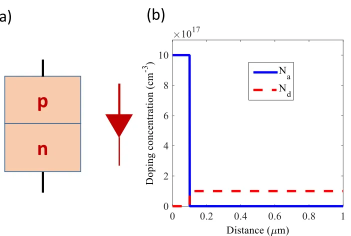
In this section, the electrical characteristics of a P-N junction in the “dark” are illustrated. A P-N junction diode is formed when a p-type semiconductor with acceptor concentration (Na), is put in contact with an N-type semiconductor, of donor concentration (Nd), as shown in Figure 1.1(a). To illustrate the behavior of P-N junction in the dark and illustrate its electrical characteristics, simulations were performed using a Physics-Based Software PC1D, which solves the Poisson’s and drift-diffusion equations [8]. The P-N junction is assumed here as In0.49Ga0.51P,
which is a standard material used in the fabrication of high-efficiency solar cells [9-11], and several solar cell structures/designs in this dissertation are based on this material. The thickness of
p-Figure 1.1: (a) schematic of p-n junction, (b) doping concentration profile of InGaP p-n junction.
p
n
3
In0.49Ga0.51P emitter, xp, is 0.1 µm. The thickness of n- In0.49Ga0.51P base, xn, is 1 µm. The p-In0.49Ga0.51P is doped with an Nd of 1018 cm-3 and the n- In0.49Ga0.51P is doped with a Na of 1017 cm-3, as shown in Figure 1.1(b).
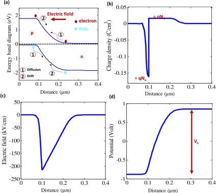
When the P-type semiconductor is put in contact with the N-type semiconductor, holes will diffuse from the P-type to N-type, as shown in Figure 1.2(a). The diffusion of holes from P-side to N-side
Figure 1.2: Schematics of In0.49Ga0.51P p-n junction at thermal equilibrium (zero-bias/without illumination): (a) Energy band diagram, showing the drift and diffusion carriers’ components. The horizontal black dotted line is the Fermi level, (b) charge density within space charge region, (c) electric field distribution, and (d) electrostatic potential. Simulations were performed using PC1D.
0 0.1 0.2 0.3 0.4
-0.15 -0.1 -0.05 0 0.05
Distance from front (m)
C h ar g e d en si ty ( C /c m 3 )
0 0.1 0.2 0.3 0.4
-250 -200 -150 -100 -50 0 50
Distance from front (m)
E le ct ri c fi el d ( k V /c m )
0 0.1 0.2 0.3 0.4
-1 -0.5 0 0.5 1
Distance from front (m)
P o te n ti al ( V o lt ) (a) (b) (c) (d) Vo
= qNd
= qNa
0 0.1 0.2 0.3 0.4
-2 -1 0 1 2
Distance from front (m)
E n er g y b an d d ia g ra m ( eV
) Electric field
p n 1 1 2 2 electron Hole 1 2 Diffusion Drift Distance (µm)
Distance (µm) Distance (µm)
4
results in two effects. First, depletion of the P-side of free carriers up to a distance, Wp; where Wp
is the depletion region or space charge region on P-side [12]. Second, the formation of an uncompensated negative acceptors’ charge on the P-side, equal to qNa, as shown in Figure 1.2(b),
where q is the elementary charge [12]. Similarly, electrons diffuse from the N-type to P-type leaving behind uncompensated positive donors’ charge (qNd) across a space charge region (Wn),
as shown in Figure 1.2(b). As a result, an electric field is formed with a direction from N-side to P-side as shown in Figure 1.2(a) and Figure 1.2(c). This electric field prevents further diffusion of majority carriers and results in a drift of minority carriers across the junction; i.e., holes, drift from N-side to P-side and electrons, drift from P-side to N-side. The thermal equilibrium state, shown in Figure 1.2(a), is reached when the diffusion of the majority carriers is balanced by the drift of the minority carriers. As a result, the Fermi energy level is flat across the P-type and N-type as shown in Figure 1.2(a). It is worth pointing out that the source of the minority carriers in the equilibrium state is the thermal generation/excitations of electron-hole pairs. The bending of the energy band diagram of Figure 1.2(a), corresponds to the difference between the Fermi level on the N-side and P-side before contact. The potential difference between N-side and P-side, shown in Figure 1.2(d), is called built-in potential or contact potential, Vo. The total depletion region width, W, on the P- and N-sides is directly proportional square root of Vo, i.e, W.
5
reduction in the potential barrier, and thus further enhancement in minority carrier concentration. If the negative terminal of the battery is connected to P-type, the P-N junction is considered in a reverse bias mode [12]. Schematics of band profiles and carrier densities for an In0.49Ga0.51P p-n junction at zero bias and reverse bias are shown in Figure 1.3 (c)-(d). The potential barrier across the P-N junction increases to Vo+Vb, thus the reducing the probability of electron diffusion from N-Side to P-side, as shown in Figure 1.3(c). Similarly, the hole diffusion from N-side to P-side is significantly reduced. Thus, the minority carrier concentration at reverse bias is about the same as the zero-bias case, as shown in Figure 1.3(d). Therefore, the dominant current component in the reverse bias mode is the drift current. Electrons will drift from P-side to N-side to become a majority, as shown in Figure 1.3(c). Similarly, holes can drift from N-side to P-side, as shown in
Figure 1.3: (a) Band profiles and (b) carrier densities for an In0.49Ga0.51P p-n junction at zero bias (blue) and forward bias (red). (c) Band profiles and (d) carrier densities for an In0.49Ga0.51P p-n junction at zero bias (blue)and reverse bias (red). The arrows in Figures (a) and (c) show the direction of the electron and hole transport following forward and reverse bias.
0 0.1 0.2 0.3 0.4
-2 -1 0 1 2
Distance from front (m)
E n er g y b an d d ia g ra m ( eV ) Zero bias + 1.2 V bias electron
Hole
Vo
Vo-1.2
(a) (b)
0 0.1 0.2 0.3 0.4
10-20 100 1020
Distance from front (m)
C ar ri er c o n ce n tr at io n ( cm -3 )
Zero bias, e density + 1.2V bias, e density Zero bias, Hole density + 1.2V bias, Hole density
Minority Carrier increase
0 0.1 0.2 0.3 0.4
10-20 100 1020
Distance from front (m)
C ar ri er c o n ce n tr at io n ( cm -3 )
zero bias, electron density -1.2 V, electron density zero bias, hole density -1.2 V, hole density
Almost no change
0 0.1 0.2 0.3 0.4
-2 -1 0 1 2 3
Distance from front (m)
E n er g y b an d d ia g ra m ( eV ) Zero-bias -1.2 bias Vo
Vo+1.2
electron
Hole
(c) (d)
Distance (µm) Distance (µm)
6
Figure 1.3(c). However, since the electrons on the P-side and holes on the N-side are minority carriers arising from the thermal excitations, the drift current is very low if compared with the current in the forward-bias mode[12]. The reverse bias will also increase the electric field across the P-N junction and widens the depletion region, W [12].
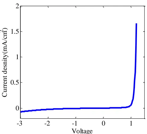
The measured dark current-voltage (I-V) characteristics of an InGaP P-N junction that will be discussed further later in this dissertation, is shown in Figure 1.4. At forward voltages higher than ~ two-thirds of Vo, the boost in the minority carrier concentration, shown in Figure 1.3(b), results in a large increase in the current. At reverse bias, the current, mainly due to the drift of thermally excited minority carriers, is very low. The current-voltage characteristics can be described using a two-diode model as follows [7],
1 2
1( 1) 2( 1),
b b
qV qV
n kT n kT
o o
I =I e − +I e − (1.1)
where the first term represents in the recombination in the neutral region (n1= 1) and the second
term represents the recombination in the depletion region (n2 = 2), Io is the reverse saturation
current due to n1 and n2, k is Boltzmann constant. When recombination occurs in neutral region
dominates, the first term of Eqn. (1.1) dominates. Similarly, the second term dominates when Figure 1.4: Measured dark current-voltage characteristics of InGaP p/n junction, grown and
processed at NCSU.
-3 -2 -1 0 1
0 0.5 1 1.5 2
Voltage
C
u
rr
en
t
d
es
n
it
y
(m
A
/c
m
7
recombination in depletion region dominates. The latter is the so-called Shockley Read Hall recombination which is dominant in the solar cells presented in this dissertations. The two-diode model is used later in this dissertation to understand the type of recombination mechanism occurring in the solar cell.
1.2.
P-N Junction under Illumination
In this section, the behavior of the P-N junction under solar illumination is discussed. The Sun is a broadband emitter that acts as a near blackbody with a temperature of ~6000K. The emission of the Sun is maximum in the visible spectrum range, 300-750 nm. The solar irradiance spectrums, AM1.50 and AM1.5, are shown in Figure 1.5 [13]. AM0 corresponds to the solar spectrum in space and has an integrated power density of ~ 1360 watt/m2. AM1.5 and AM1.5D correspond to the solar spectrum at a latitude of 48.2. AM1.5G includes both direct and diffuse sunlight, and it has an integrated power density of 1000 watt/m2. AM1.5D corresponds to the direct solar spectrum, and it has an integrated power density of 900 watt/m2. The AM0 is a standard measurement for space applications, while AM1.5G and AM1.5D spectrums are more commonly used for terrestrial applications. The AM1.5G spectrum is used for the rest of the analysis performed in this Chapter.
8
When the P-N junction is illuminated with photons of energies higher than or equal to the bandgap,
Eg, electron-hole pairs are generated in the neutral and space charge regions of the P-side and N-Side, as shown in Figure 1.6. Upon illumination. the P-N junction is not considered at equilibrium and the Fermi level is not flat as previously shown in Figure 1.2(a). Instead, the electron and hole Fermi levels split in the p-type and n-type into quasi-levels [7] as shown in Figure 1.6(b). If the P-semiconductor absorbs the incident photon, a minority electron and a majority hole will be created
Figure 1.6: (a) Illuminated P-N junction, (b) energy band diagram and (c) carrier densities for illuminated InGaP p-n junction. The arrows in Figure (b) show the direction of the electron and hole transport following photo-generation.
p
n
(a)-0.1 0 0.1 0.2 0.3 0.4
-2 -1 0 1 2
Distance from front (m)
E n er g y b an d d ia g ra m ( eV ) p n Efn Efp electron Hole Electric field (b)
0 0.1 0.2 0.3 0.4
10-10 100 1010 1020
Distance from front (m)
C ar ri er d en si ty ( cm -3 ) Equilibrium Illuminated Minority Carrier increase (c)
E >> Eg
Distance (µm)
9
in conduction and valence bands, respectively. Similarly, if the photon was absorbed by the N-semiconductor, a minority hole and a majority electron will be created in the valence and conduction bands, respectively. This results in a major increase in the minority carrier concentration at the P-side and N-side as shown in Figure 1.6(c) [7]. The built-in electric field, in the P-N junction, is directed from N-side to P-side, as shown in Figure 1.6(b). Hence, this field will prevent the majority carriers from diffusing across the junction. On the other hand, this field will sweep the minority electrons from side to N-side and the minority holes from N-side to P-side. The arrows in Figure 1.6(b) show the direction of the electron and hole transport following photo-generation. In order for this to occur, the minority carriers should diffuse to the junction; and this will depend on the diffusion length, L= D ; where D is the diffusion coefficient and
is the minority carrier lifetime. Hence, this does impose restrictions on the material quality. This
means that, for example, if a minority electron in the P-side has a long diffusion length, it will reach the junction before recombining and be swept by the electric field and contribute to the photo-current.
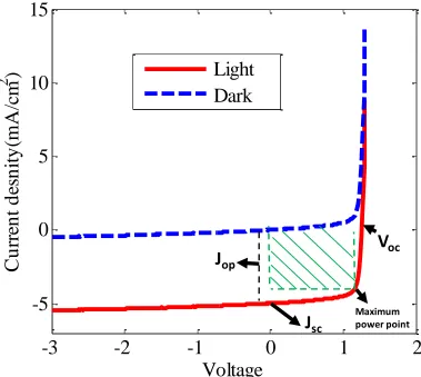
The measured current-voltage (I-V) characteristics, under AM1.5 illumination, of an In0.49Ga0.51P P-N junction that will be discussed further later in this dissertation, is shown in Figure 1.7. The current-voltage characteristics can be thus being updated as follows [7],
1 2
1( 1) 2( 1)
b b
qV qV
n kT n kT
o o op
I =I e − +I e − −I , (1.2)
where Iopis the optically generated current, which causes the current-voltage diagram to be shifted
downwards by Iop at all biases.
There are a few figures of merit for characterizing any photovoltaic devices. These metrics can be used to compare different solar cell structures/designs.
- Short circuit current (Jsc), which is the current generated in the P-N junction upon illumination at zero bias, due to the optical generation of carriers, as shown in Figure 1.7. - Open circuit voltage (Voc), which is the extracted voltage from the solar cell when there is
10
in the neutral region, i.e. n = 1, Voc can be expressed as follows [7],
1
ln sc 1 oc
o
I kT V
q I
= +
(1.3)
If the recombination is more effective in the depletion region, i.e. n = 2, Voc can be expressed as follows,
2
2
ln sc 1 oc
o
I kT V
q I
= +
(1.4)
- Maximum power point is the operating point of the cell that can maximize the electrical power, Figure 1.7. The output power is zero at the open-circuit and short-circuits conditions.
Figure 1.7: Measured dark and illuminated current-voltage characteristics of In0.49Ga0.51P p-n junction. The figure also shows the metrics that are used to assess the solar cell performance, Voc, Jsc, and maximum power point.
-3
-2
-1
0
1
2
-5
0
5
10
15
Voltage
C
u
rr
en
t
d
es
n
it
y
(m
A
/c
m
2
)
Light
Dark
V
ocJ
sc Maximum power point11
- Fill factor (FF), is a parameter which determines the maximum output power from the cell. Graphically, FF is the area of the maximum rectangle that fits in the current-voltage curve of the solar cell, as shown in the shaded green area in Figure 1.7. The FF can be expressed as follows [7],
mp mp
oc sc V I FF
V I
= (1.5)
A high series resistance and/or low shunt resistance will degrade the FF.
- Cell efficiency (η), is the fraction of the output electrical power generated by the solar cell and the incident power on the cell, Pinc. η can be expressed as follows [7],
.
oc sc
inc
FFV J P
= (1.6)1.3.
Losses in Single-junction Solar Cells
There are two fundamental losses in solar cells: sub-bandgap losses and thermalization losses. If a photon of energy equals to bandgap (Eg), shown in Figure 1.8, is incident on the P-N junction, it will be absorbed by the P-type semiconductor and will generate a minority electron in the conduction band and will be swept by the electric field. If the incident photon’s energy is less than the bandgap, shown in Figure 1.8, both the P-type and N-type will not absorb it, and this is considered as “sub-bandgap losses”. Photons of energies much higher than the bandgap will generate electron-hole pair with energy separation equal to the energy of the incident photons. The minority carriers will relax and lose their energies to the lattice in the form of heat, then will be swept across the junction by the electric field, as shown in Figure 1.8. The difference between the photon’s energy and the bandgap is considered as “thermalization losses”. Schematics that
12
Hall recombination losses are neglected. The thermalization and sub- bandgap losses of the 1.1 eV silicon cell are 34.8% and 14.72%, respectively, which result in total losses of 49.52%, as shown in Figure 1.9(a). This will correspond to an ultimate efficiency of 50.48% which considers only the thermalization and sub-bandgap losses. If other losses such as the radiative-recombination and Shockley Read Hall recombination, this efficiency value will be more reduced. The 1.7 eV P-N junction has less thermalization loss (15.1%) and higher sub-bandgap loss (45.6%) due to its higher bandgap as shown in Figure 1.9(b), thus resulting in a combined total loss of 60.46%.
The analysis discussed in Figure 1.9 wa s further extended to calculate the thermalization and sub-bandgap losses for single p-n junctions with various sub-bandgaps, Figure 1.10. The thermalization and sub-bandgap losses decrease and increase, respectively, with the increase of the bandgap as shown in Figure 1.10. The thermalization losses decrease with the bandgap increase because the energy generated from absorbed photons reduce with the increase of Eg. The sub-bandgap losses
increase with the bandgap increase as shown in Figure 1.10 because a wider region of the solar Figure 1.8: Energy band diagram of a PN junction with incident photons of energies higher
than, equal to, or less than the bandgap, showing both the thermalization and sub-bandgap losses that exist in single-junction solar cells.
-0.1
0
0.1
0.2
0.3
0.4
-2
-1
0
1
2
Distance from front (
m)
E
n
er
g
y
b
an
d
d
ia
g
ra
m
(
eV
)
Electric field
E >> E
gE = E
gE << E
g1
2
1
Thermalization lossesSub-bandgap losses
2
electron
Hole
13
spectrum is not fully utilized. If both the thermalization and sub-bandgap losses are both combined using this analysis, an optimum point of minimal total losses would exist which will correspond to an ideal ultimate efficiency of 50.5% at a bandgap of ~1.1 eV, as shown Figure 1.10. If the analysis is extended to include the radiative recombination in the solar cell material, the maximum efficiency will be 30% at a bandgap of 1.1. eV [14]. The latter is the so-called the Shockley-Queisser efficiency, which represents the maximum theoretical efficiency of a single P-N junction[14].
Figure 1.9: Schematics of AM1.5 spectrum showing the thermalization and sub-bandgap
losses for single junction solar cells: (a) silicon, with an Eg of 1.1 eV, (b) subcell,
with an Eg of 1.70 eV.
14
1.4.
Multi-junction Solar Cells
In order to reduce the sub-bandgap and thermalization losses that exist in single-junction devices discussed in Section 1.3, the multi-junction solar cell concept, was demonstrated by NCSU in 1979 [15]. In a multi-junction device, multiple P-N junctions of different bandgaps are stacked on top of each other, as shown in Figure 1.11, to divide the absorption of the solar spectrum more efficiently among them. As shown in Figure 1.11, the subcell with the highest energy (Eg1) absorbs photons with energies higher than Eg1. The second highest energy subcell (Eg2) absorb photons with energies higher than Eg2 and lower than Eg1. Similarly, the bottom cell in Figure 1.11 absorb photons in the Eg3-Eg2 bandgap range. If the 1.1 eV and the 1.7 eV cell shown in Figure 1.9 are combined in a multijunction device, this will lead to a more efficient utilization of the solar spectrum as shown in Figure 1.12. Using 1.1 eV and 1.7 eV as the bottom and top cell forms the optimum bandgap combination in dual-junction with a prospective AM1.5G one-sun efficiency of 35% [16]. The thermalization loss of the 1.1eV cell in the dual-junction structure is 6.11% as
Figure 1.10: Thermalization loss, sub-bandgap loss, and total loss in ideal single-junction solar cells, versus the bandgap. The ultimate efficiency values are calculated assuming only the thermalization and sub-bandgap losses are included. The efficiency will be more reduced if radiative-recombination and SRH recombination losses are included. These calculations were performed on the AM1.5G spectrum
0 1 2 3 4
0 0.2 0.4 0.6 0.8 1
Bandgap (eV)
Limiting efficiency Total loss%
15
shown in Figure 1.12(a), which is much less than its corresponding value (34.8%) in a single-junction structure shown in Figure 1.9(a). The thermalization loss of the 1.7 eV is the same in both the single-junction and dual-junction configurations because it is absorbing the same solar spectrum window. The 1.7/1.1 dual-junction device has total losses of ~36% which are much less than the losses in the single-junction 1.1 eV (49.52%) and 1.7 eV (60.46%) solar cells. This indicates that the ideal ultimate efficiency of the dual junction 1.7/1.1 eV cell is ~64% which is much higher than any single-junction shown in Figure 1.10. As mentioned earlier, these efficiency
Figure 1.11: Multi-junction solar cell concept
Figure 1.12: Schematics of AM1.5 spectrum showing the thermalization and sub-bandgap losses for multi-junction solar cell devices: (a) dual-junction structure (1.7eV/1.1 eV), (b) six-junction structure (2.1 eV/1.7 eV/1.4 eV/1.1 eV/0.91 eV/0.7 eV).
E
g1E
g2E
g3E > E
g1E
g2< E < E
g1E
g3< E < E
g2electron
Hole
d
1d
2d
315.19%
Thermalization loss
6.11%
Thermalization loss
14.72%
Sub-bandgap loss
Total loss = 36.02% 1.7 eV
1.1 eV
1.7 eV 1.4 eV 2.1 eV
0.91 eV 0.70 eV
13.8%
Thermalization loss
1%
Sub-bandgap loss
Total loss = 14.8%
AM1.5G
1.1 eV
AM1.5G
16
values do not include the losses due to radiative-recombination and Shockley Read Hall recombination losses.
As the number of junctions in the multi-junction stack is further increased, both the thermalization and sub-bandgap losses can be reduced. A schematic of AM1.5 spectrum showing the thermalization and sub-bandgap losses for the six-junction device (2.1 eV/1.7 eV/1.4 eV/1.1 eV/0.91 eV/0.7 eV) is shown in Figure 1.12 (b). The optimum bandgap values used in the analysis of the six-junction device is designed by Geisz et al. [17]. The thermalization and sub-bandgap losses are ~14% and 1%, thus resulting in a combined loss of ~15%. The ultimate efficiency of the six-junction device is ~21 percent point higher its corresponding value in the dual junction 1.7/1.1 eV solar cell. This confirms that the inclusion of more subcells with bandgaps scanning the entire solar spectrum results in a total thermalization loss from all subcells that is much less than each in a single-junction configuration.
Figure 1.13 shows the cumulative loss in Watt/m2 as a function of wavelength from carrier thermalization to the band-edges for single-junction 1.1 eV cell, three-junction (1.87/1.4/0.7 eV),
Figure 1.13: Cumulative loss from carrier thermalization to the band edges of single-junction 1.1 eV, three-junction (1.87/1.4/0.7 eV), and six-junction (2.1 eV/1.7 eV/1.4 eV/1.1 eV/0.91 eV/0.7 eV) devices. The integrated power density of AM1.5G is 1000 watt/m2
Lost power = 294 W/m2
Lost power = 224 W/m2
17
and six-junction (2.1 eV/1.7 eV/1.4 eV/1.1 eV/0.91 eV/0.7 eV) devices. The incident power density of AM1.5G is 1000 watt/m2. The cumulative power lost due to thermalization in the six-junction device is ~ 118 watt/m2, which is much less than the that of the three-junction (224 watt/m2) and single junction devices (294 watt/m2). Also, covering a wider region of the solar spectrum leads to reducing the lost energy in the sub-bandgap region.
Nowadays, multi-junction solar cells based on four-junction III-V materials are the most efficiency photovoltaics technology with efficiency of 46% under high solar concentration [9, 11, 18]. Five (or more) junctions are the next-generation devices with a prospective efficiency higher than 50% under high solar concentration [17]. In this dissertation, a novel subcell with a bandgap of 1.7 eV is developed for potential use next-generation five (or more) six junction devices as will be discussed later in the next few chapters.
1.5.
Research Objectives
In multi-junction solar cells, subcells with optimal bandgaps, as indicated by modeling [19-23], typically do not attain the same lattice constants. Direct growth of materials with different lattice constants result in detrimental dislocations which lead to an increased dark current and
Figure 1.14: Quantum well solar cells barrier
QWs
well
n-type
p-type Tunneling
electron
Hole
Tunneling18
reduced Voc, FF and η [24]. In addition, multi-junction solar cells seek to have an excellent current match between subcells or add more subcells to divide the solar spectrum evenly [25, 26]. Hence, an ideal multi-junction solar cell will have minimal defects with the identical current generated from each subcell. There are three main approaches to overcome the material quality and lattice-matching limitations: wafer bonding/ mechanical stacking, metamorphic growth, and the inclusion of quantum wells (QWs). Details about each approach will be highlighted later in Chapter 2. This dissertation focus on the use of quantum wells, as an alternative promising approach to realize multi-junction solar cell structures with optimal bandgaps without violating the lattice-matching condition [27]. Quantum wells are periodic nanostructures that consist of a low bandgap material, well, sandwiched between two higher bandgaps, barriers. Schematics of a generic quantum well structure is shown in Figure 1.14. Carriers generated in the quantum well region and neutral regions are transported by the electric field by thermal escape or by carrier tunneling as shown in Figure 1.14.
This dissertation proposes a novel QW structure based on InGaAsP/InGaP material system to realize a subcell in the 1.6-1.8 eV bandgap range. This QW solar cell can be part of next-generation five (or more) junction devices that will have a prospective efficiency of higher than 50% under solar concentration. Two quantum well designs are proposed in this dissertation. In the first design, the carriers are transported thermally by an electric field, while carriers tunnel across the barriers by the electric field in the second design as shown in Figure 1.14.
Chapter 8 of this dissertation focuses on a new concept for enabling photon recycling in multi-junction solar cells, in a two-terminal device configuration. This approach is based on recent research efforts in Bedair’s lab that focus on developing two-terminal tandem solar cells of two
19
1.6.
Synopsis of Dissertation
This dissertation explores the development of novel quantum well material systems and designs to advance the performance of III/V multijunction solar cells. Two quantum well structures and designs are developed.
Chapter 2 discusses the principles of quantum well solar cells, including our modeling of the band-gap tunability, critical layer constraints, strain-balance design, and carrier transport.
Chapter 3 presents a brief literature review of recent progress in the development 1.1-1.3 eV InGaAs/GaAsP and > 2.2 eV InGaN/GaN quantum well solar cells. The motivation of the development each of these QW solar cell structures will be presented.
Chapter 4 focuses on details about the growth of strain-balanced InGaAsP/InGaP quantum well structure. The growth conditions to strain-balance this QW structure are presented in this Chapter.
Chapter 5 discusses the solar cell results of strain-balanced InGaAsP/InGaP quantum. The effects of well thickness, well number, and barrier heights on the performance of this QW structure are presented in Chapter. The carrier transport of this QW structure is discussed.
Figure 1.15: Schematic of photon dynamic in multi-junction cells with an ideal reflector placed at the back of the top cell. Antireflection coatings (ARCs) are not shown for simplicity. This will be experimentally realized using the using the Inter-Metallic Bonding (IMB) Approach [28]
Back metal reflector
high Eg1Photons reflector /
Low Eg2photons transparent
Top cell (Eg1)
Bottom cell (Eg2)
h
1 1h
h
h
Top cell reflector
e h e h
e
20
Chapter 6 focuses on the growth of lattice-matched InGaAsP/InGaP quantum well structure. Details about the in-situ curvature monitoring and X-ray diffraction results are presented in this chapter as well.
Chapter 7 discusses the solar cell results of lattice-matched InGaAsP/InGaP quantum well. The carrier transport in this QW structure is also discussed.
Chapter 8 presents the concept for the development of photon-recycling in multi-junction solar cells using the inter-metallic bonding approach.
21
Chapter 2: Principles of Quantum Well Solar Cells
This chapter provides an overview of the physics of quantum well solar cells. The advantages of using quantum well structures in multi-junction solar cells are first discussed. Research needs that open up avenues for developing the next-generation quantum wells are presented in Section 2.1. Quantum well solar cells have a wide tunable bandgap, thus making them potential candidates for subcells in next-generation multi-junction solar cell devices. This bandgap tunability advantage is discussed in Section 2.2 by modeling the quantum size and strain effects in quantum well structures. The challenges related to materials growth such as critical layer thickness (CLT) and strain-balance constraints are discussed in Section 2.3 and Section 2.4, respectively. The physics of carrier transport in quantum well solar cells is presented in Section 2.6. The discussions in this Chapter is focused on reviewing the strain-balanced InGaAs/GaAsP and strained InGaN/GaN quantum well structures which are two widely researched in the last few years. In Chapters 4, 5, 6, 7: novel strain-balanced and lattice-matched InGaAsP/InGaP quantum well solar cells are presented.
2.1. Motivation
There has been an intensive search for high-efficiency photovoltaics since the invention of first p-n silicon solar cells in the 1950s [29]. Among all alternative photovoltaic technologies, the III/V multi-junction solar cells are the most efficient photovoltaic technology nowadays [5, 30]. Inverted metamorphic ( IMM) InGaAsP/InGaAs and lattice-matched InGaP/GaAs dual-junction have realized one-sun efficiencies (η) of 32.6% and 31.6%, respectively [5, 31]. Lattice-matched InGaP/Ga(In)As/Ge and IMM InGaP/GaAs/InGaAs triple-junction solar cells have realized η of 44.0% and 44.4%, respectively, under high solar concentration [32, 33]. Quadruple-junction wafer-bonded [6, 11] and IMM [18] structures have demonstrated η of ~46%, under high solar concentration. Next generation multi-junction devices will have five (or more) junctions with prospective η exceeding 50% under high solar concentration [34][17].
22
dislocations which lead to an increased dark current, and reduced open circuit voltage (Voc), fill factor (FF) and η [24]. In addition, multi-junction solar cells seek to have an excellent current match between subcells or add more subcells to divide the solar spectrum evenly [25, 26]. Hence, an ideal multi-junction solar cell will have minimal defects with the identical current generated from each subcell. There are three main approaches to overcome the material quality and lattice-matching limitations: wafer bonding/ mechanical stacking, metamorphic growth, and the inclusion of quantum wells (QWs). The first approach to overcome the material quality and the lattice matching issue is the wafer bonding or mechanical stacking, which employs combining structures of different lattice constants grown on different substrates. One example of wafer bonding is InGaP (1.88 eV)/GaAs (1.42 eV)//InGaAsP (1.12 eV)/InGaAs (0.74 eV) four-junction (4J) solar cell [11], where lattice-matched InGaP/GaAs and InGaAsP/InGaAs structures were grown separately on GaAs and InP substrates, respectively. Then the two junctions are bonded to each other during processing and the GaAs substrate is lifted-off. The second approach to overcome the material quality and the lattice matching issue is the metamorphic growth, which uses a compositionally graded buffer to relieve the build-up of stress during monolithic growth in order to access subcells with optimal bandgaps that cannot be epitaxially grown without defects [9, 35]. One example of a metamorphic structure is 4J InGaP (1.8 eV)/GaAs (1.40 eV)/InGaAs (1.0 eV)/InGaAs (0.7 eV), where a compositionally graded transparent buffer of InGaP was grown to reduce the introduction of dislocations between InGaAs and GaAs subcells [9].