1
Load Pull Methodology to Characterize Class-E
Outphasing Power Amplifiers
K. Tom M. Faulkner
Centre for Telecommunications and Micro-Electronics, Victoria University, Australia E-mail: [email protected], [email protected]
Abstract—A novel load pull methodology to characterize the performance of class-E outphasing power
amplifiers is presented. The traditional analysis of the outphasing topology cannot be applied when class-E amplifiers are used because these amplifiers do not behave as an ideal current or voltage source. Unlike most other amplifier classes, class-E amplifiers require a phase modulated input signal with constant amplitude. Additionally, class-E amplifiers have non-linear transfer characteristics which are a function of the load impedance. The methodology presented here is based on finding the load locus in the load pull plane of an individual class-E amplifier. Then the performance of the two class-E amplifiers in the outphasing topology is readily obtained. The key advantage of the method is that the load pull characterization of only a single amplifier is required. The methodology is general in that any passive load combining circuit can be used and any amplifier combination can be used in the outphasing topology provided that their load pull data is available. The load locus is derived without any reference to the phase difference between the drive signals.
1. INTRODUCTION
2 well with non-constant amplitude signals used by modern wireless systems such as orthogonal frequency division and multiplexing (OFDM) and code-division and multiple-access (CDMA) [1]-[4].
Most amplifier classes achieve their highest efficiency when the amplifier is driven into saturation i.e. at maximum output voltage. The efficiency drops when the output power is backed-off. The outphasing technique introduced by Chireix [5] and the Linear Amplification using Non-linear Components (LINC) introduced by Cox [6] are designed to operate even non-linear amplifiers at saturation, irrespective of the output power. In the outphasing topology the input signal containing both amplitude and phase modulation is separated into two constant envelope phase-modulated signals that are amplified individually and then recombined in a passive power combiner. The benefit is that highly efficient nonlinear PAs, such as class-E amplifiers, can be used to amplify the constant envelope signals without distorting the signal [7]-[10]. Hence, the outphasing topology using class-E amplifiers can be used in modern wireless systems to achieve very high efficiencies.
Outphasing topology commonly employ saturated class-B or class-D amplifiers. In the traditional analysis of outphasing topology the constituent individual amplifiers are assumed to behave like ideal voltage sources [11]. However, this assumption may lead to large discrepancies between simulation and measurements particularly when class-E amplifiers are used. Here we present a methodology to incorporate the non ideal behavior of the constituent amplifiers. Additionally, the methodology can be used to characterize outphasing amplifiers both theoretically and experimentally. We also note that the methodology can be used to characterize outphasing amplifier with any kind of class operation of the constituent amplifiers.
3 non-linear transfer function, efficiency, output power, input drive phase and losses associated with the outphasing topology. The load pull methodology is also substantiated by Harmonic Balance analysis.
The proposed load locus method can be used in the design, optimisation and testing of outphasing amplifiers. It enables the designer to predict the outphasing performance from the amplifier load pull data and the combiner network. Performance optimisation is enabled by identifying the regions of the load pull plane that provide optimum performance. The combiner network can then be designed accordingly to bring the load locus to more desirable areas in the load pull plane. Once in production the amplifiers need only be tested in the region of the load locus for stability and performance.
Section II proposes the methodology to determine the operating load locus for outphasing amplifiers. This can then be used along with load pull data of a single amplifier, to derive the operating characteristics of outphasing amplifiers. In Section III the load pull analysis for a single class-E amplifier is provided. Section IV provides the analytical expression for the load locus of class-E amplifiers in the outphasing topology. Finally, in Section V the load locus is used to determine the key amplifier operating properties. The results are presented for both ideal and non-ideal class-E outphasing amplifiers. The results are also compared with an overdriven class-B outphasing amplifier.
2. METHODOLOGY TO DETERMINE OUTPHASING LOAD LOCUS
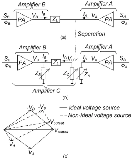
Fig. 1a shows the outphasing amplifier topology. Both amplifiers A and B are driven by square pulses with the same amplitude and frequency but with a phase difference A B. The resultant voltage
across the load ZL is determined by this phase difference. When SA and SB are in-phase the voltage difference across ZL is zero and the current through ZL is zero, so both amplifiers experience infinite load impedance. When the drive signals are 180 out of phase, maximum current flows through 0 ZL and each
4 Fig. 1. (a) Outphasing topology. (b) Analysis technique using amplifier A and composite amplifier C (c) Ideal amplifier (solid line) and practical amplifier (dashed line).
equations [6]. However, class-E amplifiers do not behave like ideal voltage sources and the output voltage and phase shift through each amplifier are no longer the same as shown in Fig. 1(c). The amplifier that is phase advanced often provides the most power and the resulting output voltage can no longer be predicted by the LINC equations. So the traditional analysis of outphasing amplifiers does not apply to class-E amplifiers. Instead a load pull methodology is proposed as outphasing can be considered as a load modulation technique.
The proposed load pull methodology to characterize outphasing amplifiers is defined in five steps.
1. Determine the load pull data (output voltage contours) of one of the constituent amplifiers in the outphasing topology, say amplifier A in Fig. 2b.
5 3. A valid operating point occurs when the impedance and output voltage of both amplifiers A and
C are the same i.e. |VA | = |VC | and ZA = ZC.
4. Repeat steps 1-3 to determine the operating point for different voltage and impedance values. The load locus is then obtained by joining the points that satisfy the condition in step 3.
5. Plot the load pull power contours for one of the constituent amplifiers, amplifier A or B. Superimpose the load locus on the load pull power contours to determine the output power of the constituent amplifiers. Other amplifier characteristics like efficiency, losses and drive phase can be obtained similarly.
In this methodology, amplifier B is combined with the load ZL to form the composite amplifier C as shown in Fig. 1(b). If amplifier A is separated from amplifier C and terminated with a load ZA, which is adjusted to maintain the same current IA and voltage VA, amplifier A will not notice the difference. That is, it will not see any change in its operating condition, since VA is completely defined by IA and ZA as VA =
ZAIA. Similarly, amplifier C, which includes the load ZL, sees no change if ZC is selected such that IC = IA
and VC = VA. Please note the different reference directions for IA, the current out of amplifier A, and for
IC, the current into amplifier C. If the load pull characteristics of both amplifiers (A and C) are obtained experimentally, then the measured impedance values of one amplifier must be negated to account for the change in direction of the reference current. However, in this analysis the negation is automatically covered by the circuit conventions in the derivation of the [VC, ZC] characteristics.
In the load pull analysis of amplifier A, ZA should cover all values that are expected to be experienced by amplifier A in the outphasing topology. Also the load pull range of amplifier C must cover the same values. At equilibrium, the load pull voltage and impedance must be the same for both amplifiers on either side of the separation. Therefore, the equilibrium conditions are given by
|VA | = |VC | (1) and
6 Fig.2. (a) Class-E Amplifier. (b) Drive signal. (c) Voltage across transistor. (d) Output voltage.
Note that we only need to consider the peak voltage value since both signals have different phase references (SA for VA and SB for VC). A valid operating point for amplifier A occurs when the |VA | load pull contour intersects the load pull contours of amplifier C where |VA | = |VC | and ZA = ZC. The operating load locus for each amplifier can then be obtained by determining all intersection points. The load locus describes the amplifier operating point for different outphasing conditions. Note that the analysis technique can work with output power contours as well. The load locus can then be superimposed on the load pull data of single amplifier A to derive the non-linear transfer function, efficiency, output power, input drive phase and losses associated with the outphasing topology. In this analysis with the LINC topology of Fig. 1(a), the load ZL is a series impedance. However the method also works if shunt
admittances are present.
3. LOAD PULL ANALYSIS OF SINGLE CLASS-E AMPLIFIER
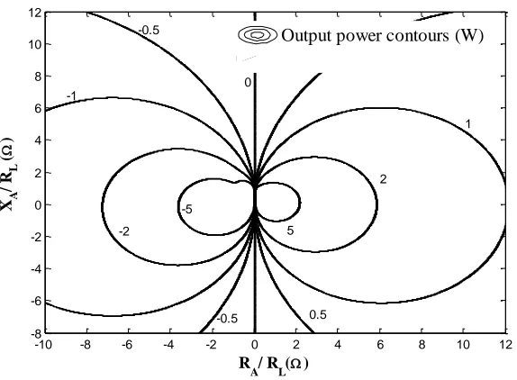
7 Fig. 3. Class-E output power contours as a function of normalised load impedance (normalised to the nominal design load resistance, RA=RL (3).
and drain voltage. The load resistance is RA. A high efficiency can be achieved by keeping the voltage-current overlap across the transistor as small as possible.
In the analysis presented here, the residual reactance XA is considered a part of the load network i.e.
ZA=RA+ jXA. Let VA, be the voltage across ZA and φA, the phase across it. Following Raab’s analysis [8]
equations for φA and VA can be written as a function of the load ZA given by
A
F Z
0
A (3)
V
A
F Z
1
A (4)where functions F0, F1 and its derivations are provided in Appendix (A8) and (A9).
To illustrate the load pull analysis, a Class-E amplifier is analyzed at an operating frequency of 1 GHz using the design equations of [8]. The selected component values are y = 2, C0 = 0.381 pF, L0 = 66.5 nH, Vdd = 5.8 V, C = 10 pF, XA = XL = 4.03 Ω, RA = RL = 3 Ω, RFC = 40 nH, and Idd = 0.877 A. The load
R
A/ RL()
XA
/
RL
(
)
-10 -8 -6 -4 -2 0 2 4 6 8 10 12
-8 -6 -4 -2 0 2 4 6 8 10 12
Output power contours (W)
-0.5
5
1
-5 -1
0
-0.5 0.5
-2
8 pull analysis is performed by varying the load ZA over the entire range of load values experienced by the outphasing scheme, which will be discussed further in Section IV. The load values must include capacitive values for the residual reactance XA and negative values for resistance RA, as for some drive conditions in the outphasing scheme, power flows back into the amplifier. Load pull contours of constant output power, computed from (18) in Appendix versus the normalised class-E load impedance, are plotted in Fig. 3. It is observed that the output power varies from 0 to 5 W for the entire load variation experienced by a single class-E amplifier in an outphasing topology. This load pull analysis of a single class-E amplifier can be applied in an outphasing topology as described in Section IV.
4. LOAD PULL ANALYSIS OF CLASS-E IN OUTPHASING TOPOLOGY
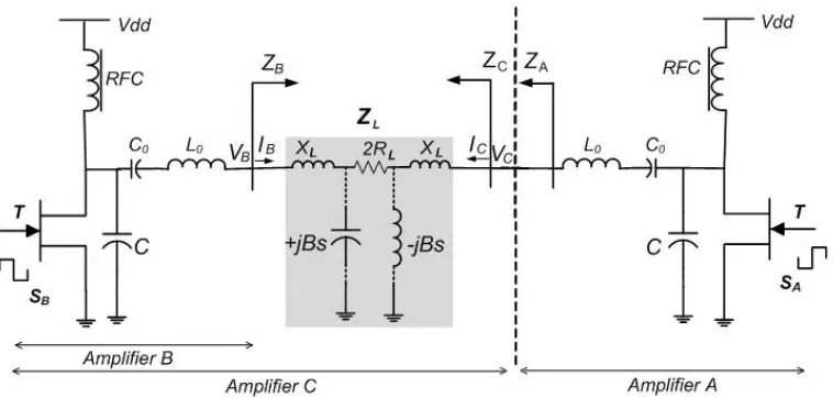
Individual class-E amplifiers in Fig. 2(a) can be combined as in Fig. 1(a) to form the outphasing topology shown in Fig. 4. The residual inductance XL and the nominal output resistance RL of each class-E amplifier is considered as part of the outphasing load ZL indicated by the shaded area in Fig. 4. Let [VB,
ZB] and [VC, ZC] be the voltage and impedance at both ends of the load and IB,IC the currents flowing into the load. A unique relationship exists between [VB, ZB] and [VC, ZC] in terms of the load reactance ZL. This relationship is obtained by solving for the load network current equations. Thus reactance ZL
transforms the load pull characteristics of amplifier B into the load pull characteristics of the composite amplifier C. In the LINC case the shunt admittances, +/-jBs equal zero, and so the current IB = - IC and the solution is given by:
B L
B C
B
Z
Z
V
V
Z
(5)
Z
C
Z
L
Z
B (6)The above two equations can be used to obtain the load pull contours of amplifier C. First, the load value
9 Fig. 4. Class-E outphasing /LINC topology. Addition of complimentary shunt reactance +jBs and –jBs (indicated by dotted line) transforms the LINC into a Chireix combiner.
(3) and (4) to calculate φB and VB. Equation (5) enables the calculation of the corresponding values of VC
at the other end of the power combiner. The output voltage of amplifier C as a function of its load is given by
1( )
C
L
C C
L C
Z
V F Z Z
Z Z
(7)
0
(
)
C
L
C C
L C
Z
F Z
Z
Z
Z
(8)
where φC represents the phase shift of Vc with respect to the drive signal SB, and comprises of the phase
shift through the amplifier B and the phase shift attributed to the power combiner network. Following the analysis presented in Section II, a valid operating point for amplifier A occurs when the |VA| load pull contour intersects the load pull contour of amplifier C where |VA | = |VC|. Substituting (4) and (7) into (1) and noting (2) provides the characteristic equation for the load locus:
1( ) 1( )
A
L
A A
L A
Z
F Z F Z Z
Z Z
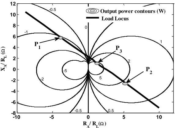
10 Fig. 5. The load locus for the class-E outphasing topology is superimposed on the Class-E output power contours. Output power is modulated by moving the amplifier operating point up and down the load locus.
The solution of the above equation provides the permissible ZA values seen by amplifier A in the LINC topology. These load values lie on a trajectory in the load pull plane of amplifier A. The expression for the load locus can be obtained by noting that ZA is a combination of RA and XA and all other parameters are constants. A numerical procedure is used to find the RA, XA combinations that satisfy (9).
5. OUTPHASING LOAD LOCUS ANALYSIS
As an example the load locus is numerically evaluated using the component values of Section III with
ZL = 2(RL + jXL), and superimposed on the output power contours of a single class-E amplifier (Fig. 3) as shown in Fig. 5. The output power is modulated along the load locus by the phase difference of the two drive signals. Please note that the analysis technique can work with output power contours as well as peak output voltage contours. Although both amplifiers operate on the same load locus, they do not operate at the same point. If amplifier A sees an impedance ZA, then from (6) amplifier B sees an impedance of ZL-ZA. The load impedance ZL for the LINC system is the same for both amplifiers and so the operating curve is symmetric around ZL/2. It is almost a straight line when plotted on linear RA, XA axes. This is not the
R
A/ RL()
XA
/
RL
(
)
-10 -5 0 5 10
-8 -6 -4 -2 0 2 4 6 8 10 12
Output power contours (W) Load Locus
-0.5
5
1
-0.5 -5 -1
0.5 -2
0
2
P
1 P
3
P
11 case for non-symmetrical circuits, such as non-identical amplifiers or a Chireix combiner, which has a capacitor to ground on one side of the load and an inductor to ground on the other side. In that case the two amplifiers generally work on different load loci.
In Fig. 5 points P1 and P2 are the operating points of amplifier A and amplifier B for a specific drive phase
of
=1350.When the drive phases are 180oout of phase each amplifier experiences the same load impedance of ZL/2 (point P3), which corresponds to optimum class-E operation in this example. When the
drives are 315 out of phase the amplifiers swap position and points P0 1 and P2 will now be occupied by
amplifier B and amplifier A respectively. The total output power is obtained by adding the individual output powers of each amplifier. Additionally, the two points on the load locus can be used to calculate the switching losses for each amplifier and the phase difference of the drive signals. The next paragraph will explain the latter point in more detail.
In this analysis VA is taken as the reference i.e. (VA) = 0. SA now has a phase shift of -φA with respect to VA. Similarly VC is made the reference for amplifier C and SB has a phase shift of -φC with respect to VC.
The phase difference
between the drives SA and SB that is necessary to give the particular valid ZAvalue on the load locus is
(
A) (
C)
(10)which is evaluated using (3) and (8):
0
(
)
0(
)
A
L A A
L A
Z
F Z
Z
F Z
Z
Z
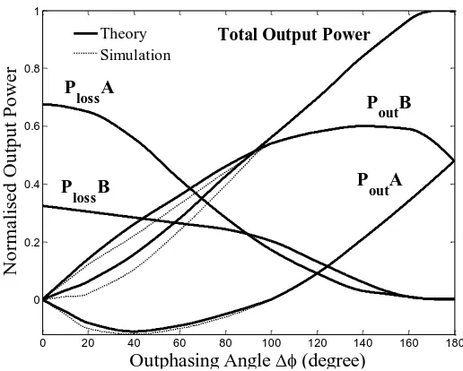
12 Fig. 6 Class-E LINC output power variation and losses for amplifier A and amplifier B across different outphasing angles. The variation in simulated output power from theory due to second harmonic content can be observed.
up to 2.5% between the theoretical values and those obtained with Agilent’s ADS HB simulator. The difference is due to the assumption in the Raab’s model of a purely sinusoidal current. In the HB analysis it was observed that the second order harmonic was significant for many drive phases. Increasing the loaded Q of the series tuned network (L0 ,C0) is not effective in suppressing these harmonics. But a wideband harmonic short to ground on either side of the load ZL proves effective in eliminating the discrepancy, Fig. 7, and theory and HB simulation agree very well.
Fig. 7. Class-E outphasing with wideband harmonic short on either side of load ZL. 0 20 40 60 80 100 120 140 160 180 0
0.2 0.4 0.6 0.8 1
Outphasing Angle (degree)
N
o
rm
a
li
se
d
O
u
tp
u
t
P
o
w
e
r
Theory Simulation
Total Output Power
P
lossA
P
lossB
P
outA
P
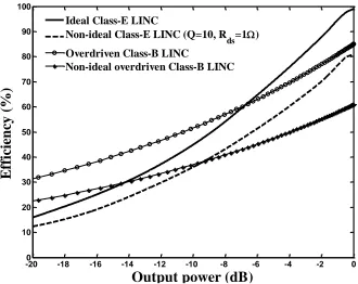
13 Fig. 8. Outphasing efficiency versus back-off output power.
The efficiency performance of the ideal class-E outphasing amplifier is compared to an overdriven idealized class-B design [3] in Fig. 8. The peak efficiency of the class-E is higher than the class-B but falls more rapidly in back-off. Class-E losses increase quickly as the impedance seen by the amplifier moves away from the optimum load. The class-E outphasing topology is therefore suitable for modulations with approximately less than 7 dB peak to average power ratios. The HB class-E curve includes non-ideal effects of finite Q and Rds resistance. There is a 20% drop in efficiency when these non-ideal effects are included. The Raab model used to derive the load pull curves in this example is a good first order approximation to the generic operation of a class-E amplifier [13]. However, it only includes switching loss, and it is this that limits the accuracy of the efficiency predictions. More inclusive class-E models do exist but they are complicated and non generic [14]-[17], i.e. they only apply to input and load combinations that give optimum class-E operation. Unfortunately, the load pull nature of outphasing amplifiers means that optimum class-E conditions are rare. A generic class-E model that is more accurate than the Raab’s model is as yet unavailable.
-200 -18 -16 -14 -12 -10 -8 -6 -4 -2 0
10 20 30 40 50 60 70 80 90 100
Output power (dB)
E
ff
ic
ie
n
cy (
%)
Ideal Class-E LINC
Non-ideal Class-E LINC (Q=10, Rds=1)
Overdriven Class-B LINC
14 6. CONCLUSION
A method for evaluating the performance of outphasing amplifier with non-ideal component amplifier, i.e. non constant voltage, is presented. To apply the methodology presented in this work, a designer must first determine the load pull data of a single amplifier either through measurement or simulation. Then through Eq. (9) the load locus of the outphasing amplifier is determined. Using this load locus and the load pull data of a single amplifier the characteristics of each of the constituent amplifiers such as efficiency, output power, gain, loss, and drive phase can be determined. This method can be applied to any amplifier combination which uses a passive power combiner provided that their load pull characteristics are available. If this information is to be provided by measurement, active load pull equipment will be necessary to measure the effect of reverse power flow.
The method is used to theoretically derive key performance parameters for the class-E outphasing topology and they are verified by analysis. The proposed methodology is substantiated with rigorous HB analysis which shows a difference of less than 2.5%. The presence of second harmonics in the HB simulations is identified as the root cause of the discrepancy.
7. REFERENCES
[1] www.ericsson.com/technology/whitepapers/sustainableenergy.pdf, accessed July 2011
[2] Larson L., Asbeck P., Kimball D.: ‘Next generation power amplifiers for wireless communications - squeezing more bits out of fewer joules’, IEEE Radio Frequency integrated Circuits (RFIC) Symposium, Long Beach, CA, USA, June 2005, pp. 417 – 420
[3] Raab F. H., Asbeck P., Cripps S., Kennington P.B., Popovic Z. B., Pothecary N., Sevic J. F., and Sokal N. O.: ‘Power Amplifiers and transmitters for RF and microwave’, IEEE Trans. Microw. Theory Tech., March 2002, vol. 50, no. 3, pp. 814-826
[4] Cripps S. C. : ‘RF Power Amplifiers for Wireless Communication’, Norwood: Artech House, 1999. [5] Chireix H.: ‘High power outphasing modulation’, Proc. IRE, Nov. 1935, vol. 23, no. 1, pp.
15 [6] Cox D. C.: ‘Linear amplification with nonlinear components’, IEEE Trans. Commun., 1974, vol. 23,
no. 1, pp. 1942-1945
[7] Zhang X., Larson L., Asbeck P.: ‘Design of Linear RF Outphasing Power Amplifiers’, Norwood: Artech House 2003.
[8] Hakala I., Choi D. K., Gharavi L., Kajakine N., Koskela J., Kaunisto R.: ‘A 2.14GHz Chireix Outphasing Transmitter’, IEEE Tans. Microwave Theory and Techniques, 2005, vol. 53, no. 6, pp. 2129-2138
[9] Wagh P., Midya P. ‘High efficiency switched –mode RF powe amplifier’. Proc. 42nd Midwest Symp. On Circuits and Systems, vol. 2, pp. 1044-1047
[10] Bassoo V., Tom K., Mustafa A. K., Cijavet E., Sjoland H., Faulkner M., ‘A potential transmitter architecture for future generation green wireless base station’, EURASIP J. Wirel. Commun. Netw., 2009, p.8. article id 821846, doi:10.1155/2009/82186
[11] Raab F. H.: ‘Idealized Operation of the Class E Tuned Power Amplifier’, IEEE Trans. Circuits and Systems, 1977, vol. 24, no. 12, pp. 725-735.
[12] Tom K., Bassoo V., Faulkner M., Lejon T.: ‘Load Pull Analysis of Outphasing Class-E Power Amplifier’, 2nd IEEE Wireless Broadband and Ultra Wideband Communications-AusWireless, Sydney, Australia, 2007, pp. 52-56.
[13] Raab F. H.: “Effects of Circuit Variations on Class E Tuned Power Amplifier,” IEEE journal of Solid State Circuits, 1978, vol. 13, no. 2, pp. 239-247
[14] Kessler D.J., Kazimierczuk M. K.: ‘Power losses and efficiency of class-E power amplifier at any duty ratio’, IEEE Trans. Circuits and Systems, 2004, vol. 51, no. 9, pp. 1675-1689
[15] Alinikula P.: ‘Optimum component values for a lossy class-E power amplifier’, IEEE International Microwave Symposium Digest, 2003, vol. 3, pp. 2145-2148
16 [17] Choi D. K., Long S. I., ‘Finite DC feed inductor in class E power amplifiers-a simplified
approach’, IEEE International Microwave Symposium Digest, 2002, vol. 3, pp. 1643-1646
8. APPENDIX
Following Raab’s analysis [13] (Fig. 2) the design equations are derived under the following assumptions:
1. The inductor RFC is lossless and large enough to neglect its ripple current.
2. The loaded quality factor of the resonant circuit (L0, C0) is high enough to ensure that the output current
iA is sinusoidal.
3. The on-resistance of the transistor Ron is zero and the transistor turns on and off instantly. The only loss mechanism is the switching loss associated with the instantaneous discharging of the capacitor C on switch closure.
The voltage across RA is sinusoidal and it can be expressed as V0
V0 sin
0
where tand
is the angular switching frequency. V0 is the peak value of the output voltage and φ0 is the phase asdefined in Fig. 2(d). The phase reference for the amplifier is set by defining the centre of the input ‘off’ pulse at 2. Similarly, the expression for the output voltage VA (θ) across ZA, is found as
VA
VA sin
A
(A1)where
2
0 1 2 0
A A
A X
V V V
R
and
2 2
1 A
A X R
.
The phase
A acrossZ
A is given by
1
0 0
tan
AA
A
X
R
17 and represents the phase shift between the voltage, VA, and the input switching drive signal, SA. The magnitude of the output voltage across ZA can be expressed in terms of the circuit parameters given by [8]:
V
A
I R
dd A
g
(A3)where Idd is the DC supply current given by
(A4)
where g is give by
0
0
2 sin
sin
2 cos
cos
2cos
sin
1
2sin
sin
sin
sin 2 cos 2
cos
2
A A A
A
y
y
y
y
y
g
y
y
y
y
(A5) and φ0 is given by0 1
2
2 1 2
cot
8 4 (1 2 )
A A
A A
C R CX
C R CX
(A6)
The output power of the class-E amplifier is given by [8]:
2 2 0 2 A dd
I g R P
(A7)
The above Raab equations are now used to calculate the amplifier’s load pull data, which includes output voltage, output power, phase shift through the amplifier and switching losses. For each value of ZA, the phase angles ,φA and φ0 are obtained fromand The capacitor C, the operating frequency ω,
and the switching period y are assumed known. Then Idd and g are calculated using (A4) and (A5) enabling the calculation of VA from (A3). Hence φA and VA can be written as
2
0 0
2
2
sin(
)
2 sin
sin
2
dd ddV
I
y
yg
y
g
y
C
18
1 0 2 2 1 2 2 tan1 cos 2 sin cos sin
tan
cos cos sin cos sin
A A
A
A A A
A A A
X F Z
R
y C R X y y y y y C R y
C X y y y y C R y X y y y y y
(A8)
2
1 2
0 0
2 sin sin 2 cos cos 2cos sin 1
1
2sin sin sin sin 2 cos 2 cos
2
A A A
A A dd A
A A
y y y y y
X F Z I R
R y y y y