Anti-Interference Circuit Configuration for Concurrent Dual-Band
Operation in High-Efficiency GaN HEMT Power Amplifier
Haruka Nishizawa, Yoichiro Takayama, Ryo Ishikawa*, and Kazuhiko Honjo
Abstract—An interference on a concurrent 4.5-/8.5-GHz-band operation has been effectively suppressed by applying a duplexer technique to high-efficiency GaN HEMT power amplifiers. Each harmonic was also suppressed by a harmonic reactive termination used for a high-efficiency operation. The developed concurrent dual-band amplifier delivered a 73% drain efficiency and a 61% power-added-efficiency (PAE) with 32 dBm output power at 8.24 GHz and a 69% drain power-added-efficiency and a 64% PAE with 37 dBm output power at 4.70 GHz. Undesired cross-modulation and intermodulation signals at nearby bands occurring due to dual-band interaction have been successfully suppressed to less than −41 dBc.
1. INTRODUCTION
Fifth generation (5G) mobile communication systems are becoming a powerful solution to the problem of increased demand for communication network capacity. In 5G systems, some frequency bands expanded from microwave to millimeter-wave have been simultaneously used to some communications. Consequently, carrier aggregation becomes one of the keywords for efficient operations, in which concurrent accesses to various ultra-fast wireless systems with sufficiently low latency are required. To realize 5G systems, difficult tasks have to be completed in power amplifier development. For power amplifiers, a multi-band concurrent operation with extremely low distortion characteristics is required, as well as a high-efficiency performance.
As high-efficiency amplifiers on a single-tone operation, class-F [1], class-E [2], and class-J [3] are well known. These are preventing an overlap between voltage and current waveforms at a transistor by controlling termination impedances at the fundamental and harmonic frequencies. For the harmonics, a reactive termination becomes a necessary condition [4, 5]. For a dual-band operation where two signals are not simultaneously input, all related frequencies have to be treated. It induces a complexity and enlargement of a matching circuit [6–8]. For a concurrent operation, since multiple fundamental frequency signals are simultaneously input, a very long time frame with beat phenomena has to be considered. In this case, a large output power back-off operation with sacrifice of power efficiency is imposed. In addition, the multiple fundamental frequency signals interfere each other, and the RF signal is distorted [9]. Such distortion contains not only the harmonic frequency components of each frequency band but also the cross- and inter-modulation frequency components for all frequency bands. Thus, even for the concurrent mode operation, at least the optimum waveforms should be retained at a transistor output electrode, and no harmonic signal should be provided to the load. Owing to the serious distortion problem, there were few papers which reported power amplifier performances evaluated by simultaneously inputting the dual-band signals and varying the input power balance to investigate the mutual interference, even though “concurrent power amplifier” was included in a title.
Overcoming this issue, a frequency duplexer concept was tentatively applied [10]. In addition, the duplexer function was embedded to the matching circuit for an MMIC integration [11]. It was
Received 13 April 2019, Accepted 5 June 2019, Scheduled 20 June 2019
* Corresponding author: Ryo Ishikawa ([email protected]).
confirmed that this concept was very effective and practical to prevent the cross- and inter-modulation though novelty of the concept is not so high. In [10], the circuit size became comparable even if the duplexer function was added, due to simplified amplifier design, in comparison with the conventional dual-band amplifier design. In this paper, to enhance the efficiency performance and decrease the circuit size more, a concurrent 4.5-/8.5-GHz dual-band amplifier that two high-efficiency power amplifiers were combined with high isolation input/output duplexer circuits was fabricated with low-loss alumina circuits. Since individual amplifiers do not deliver harmonic frequency signals to the load, the output from the concurrent dual-band amplifier delivers very low spurious signals, including harmonic frequency, cross- and inter-modulation signals, which was experimentally verified. In the verification, each band signal was almost isolated, and the spurious signals were clearly suppressed, in comparison with those of a conventional wide-band amplifier, on the concurrent operation.
2. ANTI-INTERFERENCE FOR CONCURRENT OPERATION
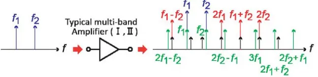
Multi-band power amplifiers have been designed based on two approaches. The first is based on multi-band impedance matching techniques which require a complicated circuit design regarding fundamental and harmonic frequency signals for a single transistor (Group I) [6–9]. The second is a wide-band amplifier design technique covering the required multiple frequency wide-bands based on Chebyshev impedance matching theory or a distributed amplifier design technique (Group II) [12, 13]. However, these approaches share a major problem, namely, suffering from poor distortion characteristics when two frequency signals are simultaneously input to a single amplifier. Figure 1 shows the schema of a distortion signal generation in conventional amplifiers due to nonlinearity of the transistor.
Figure 1. Schema of a distortion signal generation in conventional amplifiers due to nonlinearity of the transistor.
An input signal x(t) with different amplitudes and angular frequencies is represented as follows:
x(t) =A1cosω1t+A2cosω2t. (1)
Since the output yn(t) of the transistor has nonlinearity, it is represented by Volterra series expansion [14], as follows:
yn(t) =
∞
−∞h1(τ)x(t−τ)dτ +
∞
−∞h2(τ1, τ2)x(t−τ1)x(t−τ2)dτ1dτ2+. . . , (2) where hn(τ1, . . . , τn) is the Volterra kernel that corresponds to the n-th order impulse response. It is
represented by the Fourier transform of the nonlinear transfer function as
Hn(ωq1, . . . , ωqn) =
. . .
∞
−∞hn(τ1, . . . , τn)e
−j(ωq1τ1+...+ωqnτn)
dτ1. . . dτn. (3)
The output signal is obtained by the sum of the first- to nth-order nonlinear components. When nonlinear transfer functions up to the third order are calculated, the following frequency component appears:
H1:ω1, ω2
H2:|ω1±ω2|,2ω1,2ω2
H3:ω1, ω2,|2ω1±ω2|,|2ω2±ω1|,3ω1,3ω2.
When H3 is calculated considering up to the third order, H3(ω1) ∝(3A21+ 6A1A2) is derived. From
this, ω1 signal is affected by ω2 signal, which means a cross-modulation. It also induces distortion,
and it cannot be suppressed by a filter. In addition, as shown in Figure 1, if the frequencies of the modulation signals largely depart from the operation frequencies, they can be reduced by using appropriate filters. However, it is difficult to reduce the signals near the operation frequencies. As a report, the interference at a weak nonlinear region was suppressed by using shunt circuits at |ω1±ω2|
on the concurrent operation [15]. However, it was insufficient at a saturation region. Consequently, all signal paths related to the nonlinear transfer functions must be eliminated in concurrent multi-band power amplifiers.
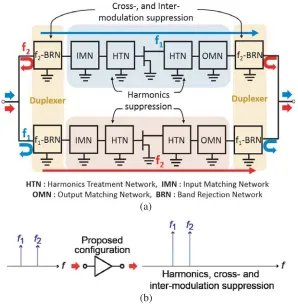
According to the above-mentioned mechanism and suggestion, an anti-interference architecture, shown in Figure 2(a), has been proposed for concurrent dual-band amplifiers. High-efficiency amplifiers at two different frequency bands with harmonic treatment circuits are arranged in parallel, and the input and output ends of each amplifier are coupled by the duplexer circuits. The different operation frequencies are rejected, and cross-/inter-modulation are rejected by the duplexer circuit. Only the fundamental frequency is input to the amplifier. In addition, harmonics are suppressed by the harmonic treatment circuit of the amplifiers. Therefore, the output frequencies from the amplifier ideally are only the fundamental frequencies, as shown in Figure 2(b).
(a)
(b)
Figure 2. (a) Anti-interference configuration and (b) spectrum on a large-signal operation for the proposed configuration.
3. DESIGN OF INDIVIDUAL COMPONENTS
designed, fabricated, and evaluated, individually in advance of the fabrication of the concurrent dual-band amplifier. All of the duplexer circuits, low-SHF dual-band amplifier, and high-SHF dual-band amplifier are fabricated with a low-loss alumina substrate (εr = 10.05, tanδ = 0.0005; substrate thickness: 0.5 mm; conductor thickness: 5µm) to improve the efficiency performance.
Figure 3(a) shows the duplexer circuit configuration. The low-loss duplexer circuit was designed to realize sufficient isolation between a f1-band port and a f2-band port with two quarter-wavelength
open stubs (λ1/4 and λ2/4) and their reactance compensation stubs. In the f1 blocking circuit, the
parallel combined impedance of the open stubs is given by Z1Z2
Z1+Z2
=−j Z01Z02cot (βλ1/4) cot (βlx1) Z02cot (βλ1/4) +Z01cot (βlx1)
(5)
Equation (5) is always zero at f1. On the other hand, it has to be open atf2. Thus,
Z02cot
2π λ2 λ1 4
+Z01cot
2π λ2l2
= 0 (6)
has to be fulfilled. Under this condition, the line from port 3 to port 1 becomes a simple 50-Ω line at f2. Similarly, the line from port 3 to port 2 also becomes a simple 50-Ω line at f1. Figure 3(b) shows
a fabricated duplexer circuit. By adjusting the characteristic impedances (Z01−04) of the open stubs,
an unnecessary attenuation pole occurring near 8.5 GHz at port 1 was moved to a lower frequency, and the low-loss 8.5 GHz pass-band was expanded. Figure 4 shows the characteristics of the fabricated 4.5-/8.5-GHz-band duplexer circuit. The minimum transmission loss at each frequency band was 0.3 and 0.4 dB at 4.51 and 8.55 GHz, respectively. In addition, high isolation was obtained between the two bands.
f2
f1 + f2
f1 λ1/4
l1 =
l1
λ2/4 l2 = l2
lx1
lx2 Open
for f1 Port3
Port1 Z0 Z0 Port2
Z02
Z01
Z04
Z03 (Z0 = 50 Ω)
Open for f2
Z1
Z2
(a) (b)
Figure 3. Designed 4.5-/8.5-GHz-band duplexer: (a) circuit configuration and (b) photograph.
For amplifier blocks in the anti-interference configuration, suppressing unnecessary frequencies is necessary, as well as realizing high-efficiency performance. Each 4.5-/8.5-GHz-band GaN HEMT amplifier constituting the concurrent dual-band amplifier was designed and fabricated based on the harmonic reactive termination technique [4, 5]. Since the harmonics are reflected to the transistor side by the harmonic reactive termination, the harmonics do not leak to the load.
Figure 5 shows the circuit configuration of the harmonic reactive termination type amplifier. For the input- and output-matching circuits in the amplifier, up to the second- and third-order harmonics were treated, respectively, by using quarter-wavelength open stubs. A GaN HEMT bare chip (CGHV1J006D, Cree Inc.) was used for the 4.5-GHz-band amplifier. The optimum impedance conditions of the input-and output-matching circuits for the transistor were estimated in load-/source-pull simulation by using Keysight ADS circuit simulator. A large-signal transistor model provided by the vender was used. For the actual circuit layout design, an electromagnetic (EM) simulation was carried out by using Keysight EMPro simulator.
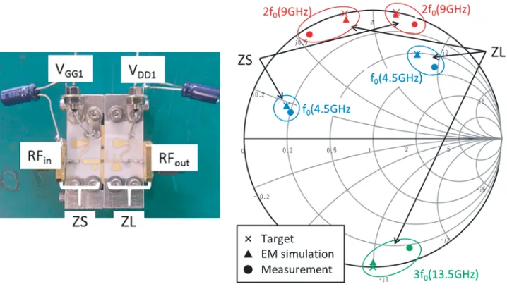
Figure 6 shows a fabricated 4.5-GHz-band GaN HEMT amplifier. In the input-matching circuit, a radial stub was used for the second harmonic termination, and a step impedance line was used for the fundamental wave matching. In the output-matching circuit, a radial stub was used for the fundamental
Figure 5. Circuit configuration of the harmonic reactive termination type amplifier.
wave matching. The simulated and measured impedance conditions for the input- and output-matching circuits are also shown in Figure 6. The optimum impedance conditions estimated by the simulation are indicated as target values. From Figure 6, it is confirmed that the simulated values derived from the EM simulation and the measured ones are close to the target values.
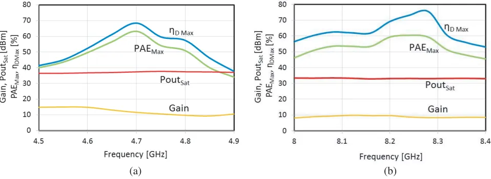
Figure 7 shows the measured frequency dependence of the maximum drain efficiency (ηDmax),
maximum power-added efficiency (PAEmax), and saturation output power for the fabricated 4.5-GHz-band GaN HEMT amplifier. The drain voltage (VDD1) and gate voltage (VGG1) conditions were set to VDD1 = 40 V, and VGG1 = −2.5 V, respectively. The fabricated amplifier exhibited an ηDmax of 73%
and a PAEmaxof 67% at 4.72 GHz with a saturation power of 37 dBm. In addition, a PAE of more than
60% was obtained from 4.66 to 4.76 GHz.
For the 8.5-GHz-band, a bare chip GaN HEMT (gate width: 96µm×10 fingers, provided by Toshiba Corp.) was used. Design and fabrication procedures for a 8.5-GHz-band GaN HEMT amplifier were similar to those for the 4.5-GHz-band amplifier. Figure 8 shows a fabricated 8.5-GHz-band GaN HEMT
Figure 7. Fabricated 4.5-GHz-band GaN HEMT amplifier, and impedance conditions of the input and output matching circuits.
Figure 9. Measured frequency dependence ofηDmax, PAEmax, and saturation power for the
8.5-GHz-band amplifier.
amplifier. The simulated and measured impedance conditions for the input- and output-matching circuits are also shown in Figure 8. From Figure 8, it is confirmed that the simulated values derived from EM simulation and the measured ones are close to the target values at the high-frequency band.
Figure 9 shows the measured frequency dependence ofηDmax, PAEmax, and saturation output power
for the fabricated 8.5-GHz-band GaN HEMT amplifier. The drain and gate voltage conditions were set to VDD2 = 20 V and VGG2 =−4.2 V, respectively. The fabricated amplifier exhibited an ηDmax of 78%
and a PAEmaxof 63% at 8.48 GHz with a saturation power of 33 dBm. In addition, a PAE of more than
60% was obtained from 8.40 to 8.50 GHz.
4. CONCURRENT MODE OPERATION FOR 4.5-/8.5-GHZ DUAL-BAND AMPLIFIER
By connecting the individually designed and fabricated duplexer circuits and 4.5-/8.5-GHz-band amplifiers, a concurrent dual-band amplifier was constructed. Figure 10 shows a fabricated 4.5-/8.5-GHz-band concurrent dual-band amplifier. Figure 11 shows the experimental setup for measuring
Figure 11. Experimental setup for measuring the concurrent mode operation.
the concurrent mode operation. To make the concurrent input signal, individual output signals from the signal generators (E4438C, Keysight and SGS100A, R&S) were combined by using the fabricated duplexer. To measure each output power at each band by using power meters (E4417A, Keysight), the output signal from the DUT is separated to each band by using the duplexer. The output spectrum signal was measured by using a spectrum analyzer (E4440A, Keysight). As a result, the characteristics of each frequency band amplifier in the concurrent mode were measured. The DC bias conditions were set to VDD1 = 40 V and VGG1 =−2.80 V for the 4.5-GHz-band amplifier, and VDD2 = 20 V and VGG2 =−4.2 V for the 8.5-GHz-band amplifier, respectively.
The measured frequency dependence characteristics of theηDmax, PAEmax, saturation power, and
gain at PAEmax for the concurrent amplifier with each one-tone input are shown in Figure 12. The
fabricated amplifier exhibited an ηDmax of 68% and PAEmax of 63% with 37 dBm output power at
4.70 GHz, and an ηDmax of 73% and PAEmax of 60% with 32 dBm output power at 8.24 GHz.
(a) (b)
Figure 12. Measured frequency dependence ofηDmax, PAEmax, saturation power, and gain at PAEmax
for the concurrent amplifier with one-tone input of (a) 4.5-GHz band and (b) 8.5-GHz band.
The measuredηDmax, PAEmax, and input-output power response characteristics for the
4.70-/8.24-GHz concurrent amplifier on a concurrent operation are shown in Figure 13(a). The fabricated amplifier exhibited an max of 69% and PAEmax of 64% at 4.70 GHz, and an ηDmax of 73% and PAEmax of 61%
5 10 15 20 25 30 35
Pout [dBm]
-40 -35 -30 -25 -20 -15 -10
Pin [dBm] Solid : f1 = 4.70 GHz Dashed : f2 = 8.24 GHz
Pin@another band is fixed to –35 dBm
–20 dBm
–15 dBm
(a) (b)
Figure 13. (a) MeasuredηDmax, PAEmaxand input-output power response characteristics for the
4.70-/8.24-GHz concurrent amplifier on a concurrent operation. (b) Measured input-output power response for a commercial broadband amplifier, as a comparison (another bandPin is fixed.).
characteristics for the commercial amplifier are shown in Figure 13(b). When another band input power was changed, the input-output power response characteristics were clearly changed due to the cross-modulation.
Figure 14(a) shows the measured output spectrum on the concurrent operation for the concurrent amplifier at the saturation output points of both bands. From the output spectrum, the harmonics and inter-modulation waves are suppressed in comparison with the fundamental frequency waves. In particular, nearby spurious signals were suppressed to less than−41 dBc. On the other hand, when the concurrent signal was applied to the commercial amplifier, relatively large spurious signals appeared, as shown in Figure 14(b), though the amplifier did not reach a saturation. Consequently, it was confirmed that the proposed anti-interference configuration was very useful and practical for the concurrent operation.
-50 -30 -10 10 30 50
Output power [dBm]
0 10 15 20
Frequency [GHz] 5
f1 f2
f1 = 4.70 GHz f2 = 8.24 GHz
Pin≈ –15 dBm
f2 f1
2f1-f2 2f
1 f1+f2
(a) (b)
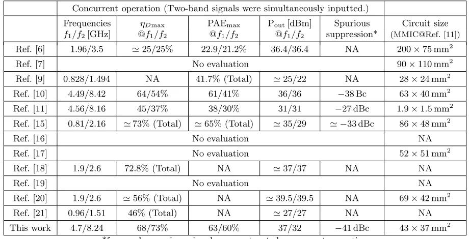
Finally, performance summary and comparison with the other concurrent dual-band amplifiers are listed in Table 1. From the comparison, good performances were obtained, especially in efficiency, since a single-band high-efficiency design could be applied in the proposed configuration.
Table 1. Performance summary and comparison with the other concurrent dual-band amplifiers.
Concurrent operation (Two-band signals were simultaneously inputted.)
Frequencies ηDmax PAEmax Pout[dBm] Spurious Circuit size
f1/f2[GHz] @f1/f2 @f1/f2 @f1/f2 suppression* (MMIC@Ref. [11]) Ref. [6] 1.96/3.5 25/25% 22.9/21.2% 36.4/36.4 NA 200×75 mm2
Ref. [7] No evaluation 90×110 mm2
Ref. [9] 0.828/1.494 NA 41.7% (Total) 25/22 NA 28×24 mm2
Ref. [10] 4.49/8.42 64/54% 61/41% 36/36 −38 Bc 63×40 mm2
Ref. [11] 4.56/8.16 45/37% 38/30% 31/31 −27 dBc 1.9×1.5 mm2
Ref. [15] 0.81/2.16 73% (Total) 65% (Total) 35/29 −33 dBc 86×48 mm2
Ref. [16] No evaluation NA
Ref. [17] No evaluation 52×51 mm2
Ref. [18] 1.9/2.6 72.8% (Total) NA 37/37 NA NA
Ref. [19] No evaluation NA
Ref. [20] 1.9/2.6 56% (Total) NA 39.5/39.5 NA 69×42 mm2
Ref. [21] 0.96/1.51 46% (Total) NA 27/27 NA NA
This work 4.7/8.24 68/73% 63/60% 37/32 −41 dBc 43×37 mm2 *for nearby spurious signals on a saturated concurrent operation
(Note that DC power cannot be separated for each frequency in Ref. [6, 9, 15, 18, 20, 21])
5. CONCLUSION
An anti-interference configuration on a concurrent dual-band high-efficiency power amplification operation was evaluated. In comparison with a commercial broadband amplifier, it was confirmed that cross- and inter-modulation can be effectively suppressed. The fabricated concurrent 4.5-/8.5-GHz-band GaN HEMT amplifier exhibited a maximum drain efficiency of 69% and 73%, and a maximum power-added efficiency of 64% and 61% at 4.70 GHz and 8.24 GHz, respectively, for the concurrent operation with a highly suppressed near-band inter-modulation signal level of less than −41 dBc in a saturated operation region.
ACKNOWLEDGMENT
This work is partly supported by the Ministry of Internal Affairs and Communications, Japan.
REFERENCES
1. Raab, F., “Class-F power amplifiers with maximally flat waveforms,”IEEE Trans. Microw. Theory Techn., Vol. 45, No. 11, 2007–2012, 2007.
2. Sokal, N. and Sokal, A., “Class E - A new class of high-efficiency tuned single-ended switching power amplifiers,”IEEE J. Solid-State Circuits, Vol. SSC-10, No. 3, 168–176, 1975.
4. Kamiyama, M., Ishikawa, R., and Honjo, K., “5.65 GHz high-efficiency GaN HEMT power amplifier with harmonics treatment up to fourth order,”IEEE Microw. Wireless Compon. Lett., Vol. 22, No. 6, 315–317, 2012.
5. Enomoto, J., Ishikawa, R., and Honjo, K., “Second harmonic treatment technique for bandwidth enhancement of GaN HEMT amplifier with harmonic reactive terminations,”’IEEE Trans. Microw. Theory Techn., Vol. 65, No. 12, 4947–4952, 2017.
6. Rawat, K. and Ghannouchi, F. M., “Dual-band matching technique based on dual-characteristic impedance transformers for dual-band power amplifiers design,”’IET Microw., Antennas Propag., Vol. 5, No. 14, 1720–1729, 2011.
7. Ji, S. H., Cho, C. S., Lee, J. W., and Kim, J., “Concurrent dual-band class-E power amplifier using composite right/left-handed transmission line,”IEEE Trans. Microw. Theory Techn., Vol, 55, No. 6, 1341–1347, 2007.
8. Enomoto, J., Ishikawa, R., and Honjo, K., “A 2.1/2.6 GHz dual-band high-efficiency GaN HEMT amplifier with harmonic reactive terminations,”Proc. European Microw. Conf., 1488–1491, 2014. 9. Takayama, Y., Uchida, K., Fujita, T., and Maenaka, K., “Microwave dual-band power amplifiers
using two-frequency matching,”’Electron. Commun. Jpn Part II Electron., Vol. 89, No. 5 17-24, 2006.
10. Enomoto, J., Nishizawa, H., Ishikawa, R., Takayama, Y., and Honjo, K., “Parallel combination of high-efficiency amplifiers with spurious rejection for concurrent multiband operation,”’Proc. European Microw. Conf., 1075-1078, 2016.
11. Ishikawa, R., Takayama, Y., and Honjo, K., “Concurrent dual-band access GaN HEMT MMIC amplifier suppressing inter-band interference,”IEEE Int. Microw. Symp. Dig., 2045-2048, 2017. 12. Wu, P-S., Huang, T-W., and Wang, H., “An 18-71 GHz multi-band and high gain GaAs MMIC
medium power amplifier for millimeter-wave applications,”’IEEE MTT-S Int. Microw. Symp. Dig., 863-865, 2003.
13. Lin, Y.-T. and Lu, S.-S., “A 2.4/3.5/4.9/5.2/5.7-GHz concurrent multi-band low noise amplifier using InGaP/GaAs HBT Technology,”’IEEE Microw. Wireless Compon. Lett., Vol. 14, No. 10, 463–465, 2004.
14. Maas, S. A.,Nonlinear Microwave and RF Circuits, 2nd ed., Artech House, Boston·London, 2003. 15. Maruyama, A., Takayama, Y., Ishikawa, R., and Honjo, K., “Linearity improvement for single-GaN HEMT dual-band power amplifier in concurrent operation mode,”Proc. Asia-Pacific Microw. Conf., 995–998, 2017.
16. Gao, S., Wang, Z., and Park, C.-W., “Concurrent dual-band power amplifier with second harmonic controlled by gate and drain bias circuit,”Proc. IEEE Int. Conf. Microw. Tech. and Computational Electromagnetics, 309–312, 2011.
17. Liu, R., Schreurs, D., Raedt, W. D., Vanaverbeke, F., and Mertens, R., “Concurrent dual-band power amplifier with different operation modes,”IEEE Int. Microw. Symp. Dig., DOI: 10.1109/MWSYM.2011.5972698, 2011.
18. Chen, X., Chen, W., Ghannouchi, F. M., and Feng, Z., “A novel design method of concurrent dual-band power amplifiers including impedance tuning at inter-dual-band modulation frequencies,”IEEE
Int. Microw. Symp. Dig., DOI: 10.1109/MWSYM.2013.6697505, 2013.
19. Zhu, S.-K., Fu, H.-P., Wu, H.-F., and Ma, J.-G., “A highly efficient concurrent dual-band class-F power amplifier for applications at 1.7 and 2.14 GHz,”IEEE Int. Microw. Symp. Dig., DOI: 10.1109/MWSYM.2015.7166915, 2015.
20. Pang, J., He, S., Huang, C., Dai, Z., Li, C., and Peng, J., “A novel design of concurrent dual-band high efficiency power amplifiers with harmonic control circuits,”IEEE Microw. Wireless Compon. Lett., Vol. 26, No. 2, 137–139, 2016.
21. Li, Y., Montgomery, B. J., and Neihart, N. M., “Development of a concurrent dual-band switch-mode power amplifier based on current-switching class-D configuration,”Proc. IEEE 17th Annual