Article
Development of laser ablation method for
fabrication of surface acoustic wave sensors
by using micro electric mechanical system
theory (MEMS)
By Eng. /Ahmed Soliman (1)* and Kukeav Alexander (2)
1-SPIE COMMUNITY, AND IEEE SOCIETY ([email protected],
2-Alexander Kukae, [email protected] (super visor of laser navigation of the project- Russia) All experiments in lab of the University of Saint Petersburg –Russia,
Abstract
:
The subject of the research is to Development of laser ablation method for Fabrication of surface acoustic wave sensors on quartz wafer, the target of the GQW – is to design Acoustic wave sensor by using laser ablation method. By using the surface acoustic wave theory to sense by the signal and using this physical phenomenon, We will design the sensor which transduce an input electrical signal into a mechanical wave which unlike an electrical signal, can be easily influenced by physical phenomena. The device then transducers this wave back into an electrical signal on the secondary terminal of the sensor. Changes in amplitude, phase, frequency, or time-delay between the input and output electrical signals can be used to measure the presence of the desired Our work in this part, especially the practical part like temperature, vibration ,etc. we design a combs on the waver of quartz to make like an electrode primary electrode & secondary electrode by putting coats of cuppers & vanadium on the waver and then using the fiber optic laser regime to design this combs to can able transfer the signal by ablation the most important here to use the regime of fiber optic laser then we using this sensor in any electronic circuit How we will select the suitable kind of laser to design, this is the most important part, and what it will be the diameter of that combs of secondary and primary , how much the value of the wave length to select the micro distant combs to avoid any inductance and interference for transferred signal , also take the benefit of using MEMS theory in our project.
Key words: sensor, acoustic wave, MEMS, laser ablation
1. Introduction
By using the surface acoustic waves theory to sense by the signal and using, that physical phenomenon [1][3], we made a sensor and develop it by using laser ablation in this part we discuss the different between the types of ablation Our work in this part and compare between laser ablation and photo lithography , especially the practical part we design a combs on the waver of quartz to make like an electrode primary electrode & secondary electrode by putting coats of cuppers & vanadium on the waver and then using the fiber optic laser regime to design this combs to can able transfer the signal by ablation, the most important here to use the regime of fiber optic laser then we using this sensor in any electronic circuit Proposed method for production of SAW-based sensors electrode topologies does not require any photo masks and, therefore, allows to make cheap small series of sensing elements. Due to the transparency of a sound conductor, it is able to create similar topologies on opposite sides of a wafer and correct already created topologies and by using the computer aided design we can design the prototype it's called OOFELIE Multiphysics to study a frequency curve and observe the transient processes in it. Obtained results are in a perfect match with experiment and theoretical predictions. This fact ensures the accuracy of the model providing a proper instrument for further multi-physical modeling, for example, the effect of different external factors, such as temperature, rotation speed, acceleration A prototype of a described delay line was produced by a laser ablation method. Due to several mistakes in the design and operation process, obtained results are unsatisfying. Nevertheless, it is allegedly that the second prototype with an increased distance between the last IDT finger and outer metallization and rotated 90° around the Z-axis will show better performance.
Proper bonding should also be performed to suppress unnecessary damage.
2. The Surface acoustic wave theory.
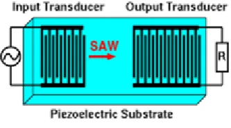
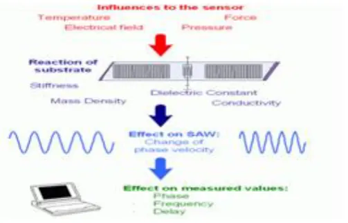
Are classes of electromechanical device which rely on the modulation of surface acoustic waves to sense a physical phenomenon [20]. The sensor transduces an input electrical signal into a mechanical wave which, unlike an electrical signal, can be easily influenced by physical phenomena. The device then transduces this wave back into an electrical signal. Changes in amplitude, phase, frequency, or time-delay between the input and output electrical signals can be used to measure the presence of the desired phenomenon. As shown in figure 1.
.
Figure 1 - Acoustic Wave Sensor,
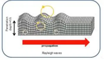
region is called the moves much slower than its electromagnetic form [21], thus causing a Delay line because the signal which is a mechanical wave at this point, appreciable delay.as shown in the figure2
Figure 2- Direction of motion of the waves
2.1. Device operation
:
.
.
(A) (b)
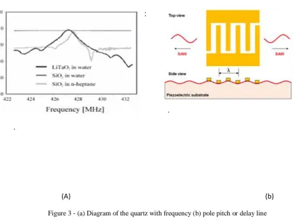
Figure 3 - (a) Diagram of the quartz with frequency (b) pole pitch or delay line
.
2.2 Parameters of acoustic service waves
The structure of the basic surface acoustic wave sensor allows the phenomena of pressure, strain, torque, temperature, and mass to be sensed. The mechanisms for this are discussed below:
2.2. A) Pressure, Strain, Torque, Temperature
The phenomena of pressure, strain, torque, temperature, and mass can be sensed by the basic device, consisting of two IDTs separated by some distance on the surface of a piezoelectric substrate. These phenomena can all cause a change in length along the surface of the device. A change in length will affect both the spacing between the interdigitated electrodes---altering the pitch---and the spacing between IDTs---altering the delay. This can be sensed as a phase-shift, frequency-shift, or time-delay in the output electrical signal When a diaphragm is placed between the environment at a variable pressure and a reference cavity at a fixed pressure, the diaphragm will bend in response to a pressure differential. As the diaphragm bends, the distance along the surface in compression will increase. A surface acoustic wave pressure sensor simply replaces the diaphragm with a piezoelectric substrate patterned with interdigitated electrodes. Strain and torque work in a similar manner, as application to the sensor will cause a deformation of the piezoelectric substrate. A surface acoustic wave temperature sensor can be fashioned from a piezoelectric substrate with a
The accumulation of mass on the surface of an acoustic wave sensor will affect the surface acoustic wave as it travels across the delay line. The velocity v of a wave traveling
through a solid is proportional to the square root of product of the Young’s modulus E and the density of the material Therefore, the wave velocity will decrease with added mass. This change can be measured by a change in time-delay or phase-shift between input and output signals. Signal attenuation could be measured as well, as the coupling with the additional surface mass will reduce the wave energy. In the case of mass-sensing, as the change in the signal will always be due to an increase in mass from a reference signal of zero additional mass, signal attenuation can be effectively used
2.3. Functionality
The inherent functionality of a surface acoustic wave sensor can be extended by the
deposition of a thin film of material across the delay line which is sensitive to the physical phenomena of interest. If a physical phenomenon causes a change in length or mass in the deposited thin film, the surface acoustic wave will be affected by the mechanisms mentioned above .
a) Chemical Vapors
Chemical vapor sensors use the application of a thin film polymer across the delay line which selectively absorbs the gas or gases of interest. An array of such sensors with different polymeric coatings can be used to sense a large range of gases on a single sensor with resolution down to parts per trillion, allowing for the creation of a sensitive "lab on a chip.
b) Biological Matter
A biologically-active layer can be placed between the interdigitated electrodes which contains immobilized antibodies. If the corresponding antigen is present in a sample, the antigen will bind to the antibodies, causing a mass-loading on the device. These sensors can be used to detect bacteria and viruses in samples, as well as to quantify the presence of certain mRNA and proteins
c) Humidity
Surface acoustic wave humidity sensors require a thermoelectric cooler in addition to a surface acoustic wave device. The thermoelectric cooler is placed below the surface acoustic wave device. Both are housed in a cavity with an inlet and outlet for gases. By cooling the device, water vapor will tend to condense on the surface of the device, causing a mass-loading
d) Ultraviolet Radiation
conducting layer. Ultraviolet radiation sensors employ the use of a thin film layer of zinc oxide across the delay line. When exposed to ultraviolet radiation, zinc oxide generates charge carriers which interact with the electric fields produced in the piezoelectric substrate by the traveling surface acoustic wave. This interaction decreases the velocity and the amplitude of the signal
f) Magnetic Fields
Ferromagnetic materials, such as iron, nickel, and cobalt, exhibit a characteristic called magneto strict ion, where the Young's modulus of the material is dependent on magnetic field strength. If a constant stress is maintained on such a material, the strain will change with a changing Young's modulus. If such a material is deposited in the delay line of a surface acoustic wave sensor, a change in length of the deposited film will stress the underlying substrate. This stress will result in a strain on the surface of the substrate, affecting the phase velocity, phase-shift, and time-delay of the signal
What is interdigitated transducer?
2.4.
Is a device that consists of two interlocking comb-shaped arrays of metallic electrodes (in the fashion of a zipper). These metallic electrodes are deposited on the surface of a piezoelectric substrate such as quartz or lithium. niobate to form a periodic structure IDTs. the primary function is to convert electric signals to surface acoustic waves (SAW) by generating periodically distributed mechanical forces via piezoelectric effect (an input transducer). The same principle is applied to the conversion of SAW back to electric signals (an output transducer). These processes of generation and reception of SAW can be used in different types of SAW signal processing devices, such as band pass filters, delay lines, resonators, sensors, etc. IDT was first proposed by White and Voltmer in 1965
a) A surface acoustic waves is (SAW)
An acoustic wave traveling along the surface of a material exhi-biting elasticity with amplitude that typically decays exponentially with depth into the substrate
.
.
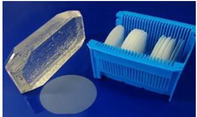
In figure 4 shows the quartz crystal shape in nature case after manipulation before any sensing technology cases or any usage in any circuits, transparent, very clear, circular style.
.
2.5.Surface acoustic wave (SAW)
Were first explained in 1885 by Lord Rayleigh, who described the surface acoustic mode of propagation and predicted its properties in his classic paper Named after their discoverer, Rayleigh waves have a longitudinal and a vertical shear component that can couple with any media in contact with the surface. This coupling strongly affects the amplitude and
velocity of the wave, allowing SAW sensors to directly sense mass and mechanical properties.
Figure 5 - Shape of the signal across the sensor
2.6.Ablation methods for preparing sensors
.
2.6.a. Laser ablation Methods using minimarkerVM2500 machine
Figure 6 - Machine of ablation mini marker 2, Uses 2-axis scanning system based on VM2500 [12]
2.7. Laser ablation
Figure 8- Copper layers Figure 7- Crystal quartz
.2.7. a).Laser ablation method
Frequency of a SAW resonator is dependent on a width of the interdigital transducers (IDT) fingers and the distance between
them .
0
λ =
V
.
f
λ
h = .
2
Where λ is a length of the acoustic wave, V is a SAW propagation velocity, f0 is a SAW frequency, h is a distance between neighboring electrodes, d is a width of the electrode. Therefore, if the one could partially remove material from IDT fingers, then the frequency of the resonator will change by a known value. This operation may be performed using a focused laser beam, the value, by which the one needs to adjust a resonator frequency, and, therefore, the amount of a material to be vapored differs from resonator to resonator. In case of mass production, this approach does not look appropriate. Thus, it is more promising to perform the whole production procedure of a sensing element using a laser. In this case, the substrate of piezo crystal is preliminary covered with a thin metal layer. There are no limitations on the thickness of this layer. It can be from 0.2 to 20 μm, etching cannot form a proper topology with this thickness (20 μm) due to a large taper of a formed structure.
λ
d = .
Another advantage of the proposed methods the ease Of new topologies formation in comparison with the photolithography method, in which you have to create a special expensive mask to produce a new topology. It is especially important in a small series production.
2.8. Layers of deposition
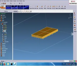
Figure 9 - Layers of deposition by modeling software
a) Vanadium (v(
It is used to increase strength and alloy hardness, deposited by amount 50 nm and it is also a good conductor.
b) Copper layer
c) Quartz electrodes after metallization
Figure 10: The process metallization by putting copper and vanadium and etching this by laser appellation as shown in [3]
.2.9. Distribution of the laser beam on the work piece
Figure 11 - Shape of distribution of the laser beam
The figures shown above describe the shape of the effects of parameters on the work piece after applying thermal conductivity and young modulus and mass density and so on to be secure during the study of the work piece properties and avoid any problems The all appears in fig numbers 1 after effecting all parameters [11],
3. Experiments in the lab
As shown in figure 15 above the device the device mini marker 2 which used the optical fiber laser light to draw and design on the surface of the metal or any surface depend on the kind laser used The "MINI Marker 2" laser machine is a high-tech, compact equipment capable of engraving products with an accuracy of up to 2.5 μm * and a speed of up to 8700 mm / s, which allows it to be in the first place among fiber laser engravers
3.1. Accessories
Fiber laser emitter from 20 to 100 Hz - allows you to apply laser engraving on metals and plastics at high speed. It can also be used for perforating and cutting sheet metal to a thickness of 0.5 mm (foil) and a hole diameter of up to 0.05 mm Z-axis - enables 3D engraving to be manufactured for various kinds of dies, molds, and dies used for casting or stamping of metal products MINI Marker 2" in LLC "Mehprom" is equipped with a swivel mechanism (razchatelem).
3.2. After coating the quartz in Lab
The shape above shown in figure 15 our work piece after applying the three layers copper and vanadium and its appear the comb drown on the both two sides which this electrodes transfer the signal from terminal to terminal, all metallization etched by laser ablation process by device named mini marker 2 which work by optical fiber laser light this work piece will work by acoustic waves to transfer the signal from primary to secondary .
We test approximately 3 quartz pics, to check if valid or not, for example the good metallization for every pics. If it is connected good under microscopy ,the best one for our work we consider it as project work one, after that we go to test the frequency range for the work shop station one , by putting on the spectrum analyzer device as shown in the ,we found transmitting arrange of frequency as shown in fig 2 as domain of frequency input on the work shop ,and monitor the frequency spectrum and the max transmitted one spike like shown across all frequencies, After finishing the sensor we will use it in gyroscope or any electronic circuit.
3.3.The first experiments In the Lab
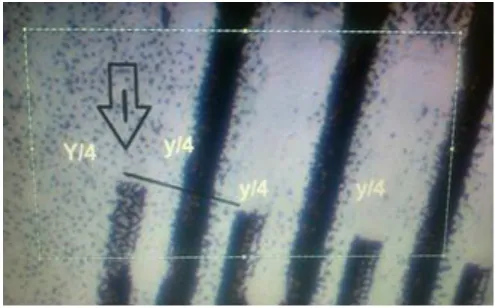
Figure 12 - Microscopic photo of the interdigited comb and pole pitch
From the equation:
C = λ .
f
Where:
C- Speed of sound
Frequency ƒ in Hz
λ -Wave length
Where the speed of the sound is C= 3500 m/s
The thickness of the quartz plates which will be used in our project approximately 1mm that mean capable to transfer approximately from 3 to 20 MHz The distance between every electrodes is equal approx. λ /4 that mean the length between to corresponding electrode = λ Like shown in figure above every electrode width equal λ /4, that mean for example if we design the frequency about 20 MHz it must wave length =200um and bydividing this λ /4 for every electrode it will equal 50 um all this to design by a good suitable way.
The second Experiment in the lab 3.4.
Figure 13 - Micro photo of the produced IDT structure
It is possible to indirectly measure the centre-to-centre distance of the IDT structure. To do this, the one needs to estimate the length of the acoustic wave in the delay line on its central frequency. Therefore, the delay line was connected to the spectrum analyzer. The results are demonstratedWe test approximately 3 quartz pics, to check if valid or not, for example the good metallization for every pics. If it is connected good under microscopy ,the best one for our work we consider it as project work one, after that we go to test the frequency range for the work shop station one , by putting on the spectrum analyzer device as shown in the fig 1 and 2after test we found transmitting arrange of frequency as shown in figure above as domain of frequency input on the work shop pics ,and monitor the frequency spectrum and the max transmitted one spike like shown across all frequencies By applying the frequency range from the spectrum analyzer device we about range from 0 to 20 MHz across the primary terminal of the work piece to check how much of frequency it will pass to the secondary electrode like the transformer exact by mutual inductance the electrical wave transferred to acoustic wave ,and then transferred again to electrical wave , to we can find the spike frequency of approximately 11.1 MHz is the most big signal transferred which is the desired one
range that mean the electrodes ,Max frequency received = 11.12
MHz
.
The second fabricated prototype 4.1.
A “MiniMarker 2”precision laser engraver with a fiber transmitter have been used to create a dual-channel delay line, described by Yan and modeled above. The topology was formed on a 128° YX-cut LiNbO3 wafer covered with 50 nm Vanadium for better adhesion, than 5 μm of Cu, and additional 50 nm of Vanadium to protect copper from corrosion. Produced delay line is shown in figure 15
Figure 15 - Produced dual-channel delay line
A dark line in a bottom part represents some metallization that was left on the opposite side of the wafer and do not affect the delay line performance. Lower IDT busses are connected to the outer metallization with a conducting glue for an easier testing. IDTs in middle were considered as inducing and a signal generator was connected to it. Side IDTs were connected to spectrum analyzer to obtain a frequency curve of each channel. Obtained results are shown in figure 16
Figure 16 - Frequency curve of a right channel (according to fig15)
1-Very high insertion loss
2-Frequency mismatch (central peak is located at about 18.5 MHz when
predicted value was 20 MHz)
3-Spread curve without a clear central and side peak
Detailed study of the DL using a microscope and a profilometer showed
that there are several damaged regions of crystal (shown in figure above,
a-c), especially in the left channel. Probably this is the reason for a high
insertion loss in the right channel and a lack of signal in the left channel as
well. As soon as Lithium Niobate is almost transparent for a used laser
wavelength (1064 nm), these scratches come from unprecise transportation
and testing process.
.
Figure 17 represents that the distance between the side IDT and the outer metallization is very small and may cause parasitic reflections, which may spread the frequency curve and additionally increase insertion loss. As for the frequency mismatch, its reason may lie in the nature of crystal wafer, e.g. its anisotropy. Wave propagation speed differs for orthogonal directions in 128° YX-cut LiNbO3 for X and Y propagation directions (3978 and 3484 m/s, correspondingly). Obtained central frequency is in a very good match if we suggest that the DL is oriented in Y direction, when the original prototype is oriented in X direction. Therefore, the frequency mismatch may come from a 90° rotation of the wafer in comparison with a prototype.
Metal film side heating 4-2.
While the film is in a liquid state the metal can spread out into the region where it is already in the solid phase (farther from the center of the radiation) due to its instability in thickness and also due to surface tension forces. Therefore, the greater
A
B
C
the melting point of the material, the closer would be the solid phase to the center of the radiation. Temperature T of the film is described using following expression
.
where q is the radiation power density, r is the radial coordinate with the origin at the center of the beam, A is the absorptivity of the film, t is the exposure time, ρ is the density, C is the heat capacity, a is the thermal diffusivity of the film, h is the film thickness, τ is the pulse width, and i2erfc is the additional probability integral. Using expression (1) we can estimate the thermal distortion pattern for three basic materials used as the film: gold, copper and aluminum. We assume that the pulse width τ = 20 ns, and the diameter of the laser spot in focus d = 20 μm. The values of the thermal distortions for different materials are shown in figure 18
Figure 18- Dependence of film temperature on the distance from the laser beam center
The presented graphs end at the points where the metallic films pass from the liquid phase to the solid phase. It is easy to see that aluminum has the greatest thermal distortion. The value where it passes into the solid phase is 0.65 μm from the edge of the beam spot. Copper and gold show noticeably better results. The latter has the maximum thermal distortion of 0.31 μm. The best result is shown by copper - 0.21um To verify obtained results finite element modeling of the laser ablation process was performed in OOFELIE::Multiphysics. The substrate was presented as 50x50 μm and 1 mm thick quartz box. It was covered by a metal film with a thickness of 400 nm. Film material varied to model three abovementioned cases. In the center of metal film a spot with a diameter of 20 μm was heated up to the boiling point. The power density was chosen so that a given temperature for each material was reached at the end of a pulse equal to 20 ns. Thus, it is possible to estimate the distribution of temperature fields over the surface, which arise due to the high thermal conductivity of a metal. Figure 19 shows modeling results for aluminum metal film. Distribution of temperatures along the beam diameter is shown in Figure 20.
2 0 0 0 2 0 0 0
1 2 erfc ,
ρ 2 τ
( , ) .
2
erfc ,
ρ 2 τ
r r r
qAt
i r r
Ch r a
T r t
r r r
qAt
i r r
Ch r a
Figure 19 - Aluminum film temperature distribution
Figure 20 - Distribution of temperatures along the beam diameter for aluminum film
Conclusion
We test approximately three quartz pics, to check if valid or not, for example the good metallization for every pics. If it is connected good under microscopy ,the best one for our work we consider it as project work one, after that we go to test the frequency range for the valid prototype , by putting on the spectrum analyzer device as shown above ,we found transmitting arrange of frequency as shown in as domain of frequency input on the work shop ,and monitor the frequency spectrum and the max transmitted one spike like shown across all frequencies, we still continue our work to finish this sensorA dual-channel delay line was simulated in OOFELIE::Multiphysics to study a frequency curve and observe the transient processes in it. Obtained results are in a perfect match with experiment and theoretical predictions. This fact ensures the accuracy of the model providing a proper instrument for further multiphysical modeling, for example, the effect of different external factors, such as temperature, rotation speed, acceleration, etc. A prototype of a described delay line was produced by a laser ablation method. Due to several mistakes in the design and operation process, obtained results are unsatisfying. Nevertheless, it is allegedly that the second prototype with an increased distance between the last IDT finger and outer metallization and rotated 90° around the Z-axis will show better performance. Proper bonding should also be performed to suppress.
References
[1] Precise Robust Inertial Guidance for Munitions (PRIGM): Advanced Inertial Micro Sensors (AIMS), Microsystems Technology Office, DARPA-BAA-15-38, May 29, (2015)
[2] Davaji B., et al. "Towards a surface and bulk excited SAW gyroscope." Ultrasonic, Symposium (IUS), 2017IEEEInternational.IEEE, (2017)
[3] Lukyanov D. P., A. Soliman, and S. Yu Shevchenko. "Design optimization of a microgyrocsope on standing surface acoustic waves." Integrated Navigation Systems (ICINS), 2017 24th Saint Petersburg International Conference on. IEEE, (2017)
[4] Lukyanov D., et al. "Experimental study of laser trimmed surface acoustic wave delay line topologies." Optical Sensors 2017. Vol. 10231. International Society for Optics and Photonics, (2017)
[5] Lukyanov D, et al. "The use of quartz packaging for SAW-based sensors." Young Researchers in Electrical and Electronic Engineering Conference (EIConRusNW), 2015, IEEENW, Russia .IEEE, (2015)
[6] So N. V., Osetrov A.V. “Calculation of the parameters of surface acoustic waves in piezoelectrics using the finite element method,” Vychislitelnaya mechanica sploshnich sred, Vol. 4, № 4, pp. 71-80 (2011) in Russian.
[7] Fu C., Elmarzia O., Lee K. “Implementation of wireless battery-free microgyrosensor by utilizing one-port SAW delay line and an antenna with double resonant frequencies,” SPIE MOEMS-MEMS.–International Society for Optics and Photonics,pp.897503-897503(2014)
[8] Oh H., et al. “Enhanced sensitivity of a surface acoustic wave gyroscope using a progressive wave,” Journal of Micromechanics and Micro engineering, Vol. 21, №. 7, (2011) .
[9] Yan Q., et al. “Theoretical and experimental study of surface acoustic wave gyroscopic effect,” Mechatronics and Automation, 2007. ICMA 2007. International Conference on. – IEEE, pp. 3812-3816 (2007)
[10] Xu F., et al. “Optimization of Surface Acoustic Wave-Based Rate Sensors,” Sensors, Vol. 1, №. 10, pp. 25761-25773 (2015)
[11] Ahmed soliman. “Multiphysical simulation of surface acoustic wave Micro gyroscope sensing elements,” MSC Thesis, St. Petersburg Electro technical University, (2016) in Russian
http://www.minimarker.ru/tech_data.php
[13] Accelerometers Based on Surface Acoustic Waves," Lukyanov D., Shevchenko Ahmed., soliman A., Filippova E., Safronov D., Proc. 32nd NORCHIP,
[14] Lukyanov D., Shevchenko S., Kukaev A., "Micro rate gyros for highly dynamic objects," Microsystem Technologies 12 (20), 2137-2146 (2014)
[15] Veiko V.P., “Laser processing of film elements". Engineering, Leningrad (1986). in Russian
[16] Liebenson M.N., Nikitin M.N., "On thermal image distortion at film processing by optical quantum generators," Material processing physics and chemistry 5, 9-13 (1970). In Russian
[17] MiniMarker2technical characteristics," Minimarker.ru, accessed August 2017. http://www.minimarker.ru/tech_data.php
[18] A micro rate gyroscope based on the SAW gyroscopic effect," Lee, S.W., Rhim, J.W., Park, S.W., Yang, S.S., J. Micromech. Microeng. 17, 1156-1159 (2007)
[19] Surface acoustic wave micro gyroscope," Lukyanov D.P., Peregudov A.N., Kukaev A.S., Shevchenko S.Yu., Shevelko M.M., RU patent № 137098, issued January27, 2014(2014)
[20] Wikipedia, acoustic wave sensors, "accessed February 2017.
https://en.wikipedia.org/wiki/Surface_acoustic_wave_sensor
[21]Fabrication of surface acoustic wave,” accessed February

![Figure 6 - Machine of ablation mini marker 2, Uses 2-axis scanning system based on VM2500 [12]](https://thumb-us.123doks.com/thumbv2/123dok_us/8041522.1338960/8.595.182.412.377.570/figure-machine-ablation-mini-marker-uses-scanning-based.webp)
![Figure 10: The process metallization by putting copper and vanadium and etching this by laser appellation as shown in [3]](https://thumb-us.123doks.com/thumbv2/123dok_us/8041522.1338960/11.595.172.378.404.560/figure-process-metallization-putting-copper-vanadium-etching-appellation.webp)