IJEDR1401210
International Journal of Engineering Development and Research (www.ijedr.org)1179
Comparative Analysis of Compensation Techniques
for improving PSRR of an OPAMP
1
Pathak Jay,
2Sanjay Kumar
M.Tech VLSI and Embedded System Design,
Department of School of Electronics, KIIT University, Bhubaneswar 1[email protected] , 2[email protected]
________________________________________________________________________________________________________
Abstract—This el The operational amplifiers are the primary blocks of most of the analog systems and mixed-signal integrated circuits. In most electronic devices, ripple noise in supply line is unavoidable. Hence a robust noise performance at high frequencies is required. This performance regarding the stability of OPAMP improves with help of frequency compensation techniques. The different compensation techniques CMOS OPAMP are Miller compensation, Cascode compensation, Blakiewicz compensation and Tail compensation. These Compensation techniques provide PSRR and stability to the OPAMP. These techniques has been done at 180nm CMOS technology, simulation and result were carried out in Cadence Spectre EDA TOOL with 1.8v power supply.
Index Terms—CMOS, Blakiewicz and Cadence Spectre EDA TOOL.
I. INTRODUCTION
All The operational amplifiers (OPAMPs) are important building blocks in modern mixed-signal microelectronic systems. The need for continuous reduction of supply voltage in systems designed using complementary metal-oxide semiconductor (CMOS) sub-micrometer technologies, makes OPAMPs attractive for analogue signal processing owing to relatively good linearity and satisfactory dynamic range. Most known OPAMPs can work properly when are used as separate analogue modules, but their performance degrades noticeable in mixed-signal systems on a chip (SoC). The main reason for dynamic range degradation is additional noise generated by digital part of a system, which propagates inside a chip along power/ground supply lines reaching sensitive analogue blocks. Typical OPAMPs have relatively good power supply rejection ratio (PSRR) at very low frequencies and highly insufficient above several hundred kilo hertz. This characteristic is especially undesirable in modern mixed-signal SoCs, where fast digital sub-systems generate broadband noise. As a consequence, the design of OPAMPs dedicated to mixed-signal SoCs can not only be limited to optimization of the unity-gain bandwidth (GB) or power consumption, but it should also be extended to improvement in broadband high rejection of power supply noise. The analysis of typical two-stage OPAMPs shows that the main reason for PSRR degradation with frequency is a compensation circuit. So several compensation techniques has been implemented which will improve the Power Supply Rejection Ratio and these all techniques are considered in 180nm technology with power supply of 1.8V.
II. TWO STAGE OPAMP
Two-stage operational amplifiers are widely used in analog systems due to their many features such as: simple biasing, large output-voltage swing and better noise performance. Two-stage OPAMPs, compared to single-stage which only drive capacitive loads, have the ability to drive capacitive and resistive loads. In general, frequency compensation is required for ensuring closed-loop stability of two-stage amplifiers. The simplest frequency compensation technique is achieved by connecting a compensation capacitor Cm between the output nodes of the two stages, thus employing the Miller effect. For an operational amplifier to be
stable, the gain must be below unity before the phase response reaches 1800. The difference between -1800and the value of the phase response at unity-gain frequency is termed as phase margin. It is an important term used to determine the stability of an OPAMP. A fast transient response with no ringing translates to a phase margin value of approximately 600. A phase margin of 400 translates to a higher amount of ringing in the time-domain. The frequency response of an operational amplifier is determined by the low-frequency gain, pole/zero locations and the number of poles/zeros. Poles and zeros are classified based on their effects on the gain and phase responses. The gain decreases at a rate of -20dB/decade and the phase response drops to 900, for LHP poles. RHP poles make amplifiers unstable. For zeros, if the magnitude response increases at a rate of 20dB/decade and the phase response goes up by 900, then it is termed as a LHP zero. RHP zeros increase the magnitude response by 20dB/decade while decreasing the phase response by 900 and tend to decrease stability of a circuit. Different compensation techniques are used to improve the stability and PSRR. In this work, we will restrict ourselves to two-stage amplifiers.
III. COMPENSATION TECHNIQUES
IJEDR1401210
International Journal of Engineering Development and Research (www.ijedr.org)1180
Miller Compensation
Miller Compensation is techniques which is widely used in OPAMPs. The implementation of Miller Compensation is shown in Fig.1.a The first stage consists of two NMOS transistors M1 and M2, connected to a PMOS current-mirror load of two transistors M3 and M4. The second stage consists of a common-source stage realized through PMOS transistor M7. A capacitor Cm is
connected between the output node and the internal node of first stage. The small signal model of Miller Compensation technique is shown in Fig.1.b.
Figure 1.a Miller Compensation Figure 1.b Miller Compensation small signal model[2]
Cascode Compensation
The Cascode Compensation technique helps in increasing the stability, phase margin and bandwidth of an amplifier through a feedback capacitor connected in series with a current-buffer. Instead of an extra current-buffer circuit, the cascoded transistor is used as the current-buffer as shown in Fig.2.a The cascoded transistor is a common-gate amplifier which has a positive gain of gm4R1 , from the source to drain terminals of transistor M4. The input impedance of the cascode transistor M4 is 1/gm4. Therefore
the overall feedback is negative. The small signal diagram of cascode compensation is shown in Fig.2.b. The compensation capacitor Cc is connected between nodes VY and VOUT.
Figure 2.a Cascode Compensation Figure 2.b Cascode Compensation small signal model[2]
Blakiewicz Compensation
The Blakiewicz Compensation technique is useful in improving PSRR widely in two stage OPAMPs[1]. Instead of placing the compensation network between the first and second stages, the compensation network is created by using a stage of two transistors and a compensation capacitor. Here the input stage is cascoded with other two extra transistors. The most important positive trait of this technique is the drastic reduction of the required value of compensation capacitor by 12 times when compared to Miller compensation technique. The Fig.3.a shows the schematic with Blakiewicz technique and Fig.3.b shows the small signal model of the schematic.
IJEDR1401210
International Journal of Engineering Development and Research (www.ijedr.org)1181
Tail Compensation
In Tail Compensation technique, the capacitor CC is connected to an internal node VX from the output node. This particular
internal node is selected because of very low impedance achieved by the source terminals of differential pair transistors M1 and M2. The output of the first stage is isolated from the feedback network by a current buffer. As in current buffer compensation schemes, there is no feed-forward path from node V1 to VOUT The schematic of these compensation is shown in Fig.4.a and small
signal model of the circuit is shown in Fig.4.b.
Figure 4.a Tail Compensation Figure 4.b Tail Compensation small signal model[2]
IV. ANALYSIS OF PSRR USING DIFFERENT COMPENSATION TECHNIQUES
In OPAMP, the PSRR at high frequencies is usually improved through increasing the dominant pole or through noise cancellation techniques. the compensation networks generally improve the PSRR through increasing the dominant pole location.
Miller Compensation
The small signal model for analyzing PSRR for a basic two-stage OPAMP using Miller Compensation technique is shown in Fig.5. The effect of change in current in the first stage due to supply voltage changes is modeled as VDD/ro1 where ro1 is the
intrinsic resistance of the differential input NMOS transistor M1 of a basic two-stage OPAMP. The parasitic capacitance at the output of first stage is modeled as C1 and the intrinsic resistance of transistor M2 is labeled as ro2. The compensation network
consisting of CC and RC is connected between nodes V1 and VOUT. The second stage is modeled as a voltage controlled current
source having value gm7 times the gate-to-source voltage, VDD-V1. The output impedance is ROUT and COUT .The effect decreased
impedance at high- frequencies, of the compensation capacitor CC leads to tracking of the gate voltage of transistor M7 to VDD It
results in a poor PSRR performance from the positive rail.
Figure 5 PSRR small signal model for basic two-stage OPAMP with Miller Compensation[2].
Cascode Compensation
The small signal model for analyzing PSRR for a basic two-stage OPAMP using cascode compensation technique is shown in Fig.6. The effect of change in current in the first stage, parasitic capacitance and intrinsic resistance is same as that of Miller Compensation. The current through cascode transistor M4 is modeled as iC going into node V1. The compensation network
consisting of: CC is connected between nodes VY and VOUT. The second stage is modeled as a voltage controlled current source of
value: gm7(VDD-V1). The output impedance is ROUT and COUT Though cascode transistor is reported to have a better PSRR
IJEDR1401210
International Journal of Engineering Development and Research (www.ijedr.org)1182
Figure 6 PSRR small signal model for basic two-stage OPAMP with Cascode Compensation[2]Blakiewicz Compensation
The positive PSRR using this compensation is calculated using the small-signal diagram as shown in Fig.7. The first stage is modeled as a voltage controlled current source gm1VIN, with R1 and C1 being the impedances of the first stage. The second stage is
modeled with the transconductance of transistor M7 being gm7 times the output voltage of the first stage, which is V1. The output
impedance is ROUT and COUT. The compensation network is placed between nodes V1 and the source node of transistor M8
modeled as gm8V1. Here, RC is equivalent to 1/gm8.The dominant pole achieved through this scheme is of a higher magnitude than
that of Miller compensation. This is because of the much smaller CC used for compensating the OPAMP, thus extending the
bandwidth of the PSRR They also report that at higher frequencies, the PSRR performance increased.
Figure 7 PSRR small signal model for basic two-stage OPAMP with Blakiewicz Compensation[1]
Tail Compensation
The small signal diagram for Tail compensation is shown in the Figure.8. The compensation capacitor CT is placed between
nodes VOUT and VX. Here too, the effect of the feedback is modeled as −gm1VX. The feed-forward path is modeled as Kgm1(VOUT
-VX). The effect of the feedback is shown through the connection of a voltage buffer of gain 1 between nodes VOUT and VX. through
the 1/gm1 source terminal of transistor M1.
Figure 8 PSRR small signal model for basic two-stage OPAMP with Tail Compensation
V. SIMULATION RESULTS OF DESIGNS
IJEDR1401210
International Journal of Engineering Development and Research (www.ijedr.org)1183
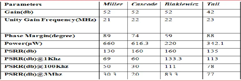
Table 1. Simulation ResultsVI. CONCLUSION
The PSRR of each techniques vary from its each other in many other aspects as considering the compensation technique of Miller compensation has an extra resistance which may increase the area of the overall OPAMP likewise in the case of an Cascode the gain may increase and also the stability related to PSRR of an OPAMP but the input range or operating voltage of an OPAMP decreases. Taking the consideration of the Blakiewicz compensation into consideration an extra additional circuit is added which give fruitful result related to PSRR but an extra circuit may leads to power and area into account. The last techniques is all about Tail compensation which is totally different from others techniques but circuitry implementation is complex. Thus with the study and analysis of various compensation techniques some other parameters are also affected by improving the PSRR. The improving of PSRR as thus increases the stability at various other analog and mixed signal circuitry.
REFERENCES
[1] G. Blakiewicz, “Frequency compensation for two-stage operational amplifiers with improved power supply rejection ratio characteristic” IET Circuits, Devices and Systems, vol.4, no. 5, pp. 458–467, Sep. 2010
[2] Paul M. Furth, Sri Harsh Pakala, Annajirao Garimella and Chaitanya Mohan, "A 22dB PSRR Enhancement in a Two-Stage CMOS Opamp Using Tail Compensation"
[3] P. Allen and D. Holberg, CMOS Analog Circuit Design, 2nd Edition. Oxford University Press, 2002. [4] B. Razavi, “Design of Analog CMOS Integrated Circuits”, New York McGraw-Hill, 2001.
![Figure 3.a Blakiewicz Compensation Figure 3.b Blakiewicz Compensation small signal model[2]](https://thumb-us.123doks.com/thumbv2/123dok_us/8445665.1388783/2.595.54.551.362.530/figure-blakiewicz-compensation-figure-blakiewicz-compensation-small-signal.webp)
![Figure 4.a Tail Compensation Figure 4.b Tail Compensation small signal model[2]](https://thumb-us.123doks.com/thumbv2/123dok_us/8445665.1388783/3.595.163.448.448.572/figure-tail-compensation-figure-tail-compensation-small-signal.webp)
![Figure 6 PSRR small signal model for basic two-stage OPAMP with Cascode Compensation[2]](https://thumb-us.123doks.com/thumbv2/123dok_us/8445665.1388783/4.595.164.460.501.625/figure-psrr-small-signal-model-opamp-cascode-compensation.webp)