Volume 2009, Article ID 738381,16pages doi:10.1155/2009/738381
Research Article
Signal Adaptive System for Space/Spatial-Frequency Analysis
Veselin N. Ivanovi´c (EURASIP Member) and Srdjan Jovanovski
Department of Electrical Engineering, University of Montenegro, Cetinjski put bb, 81000 Podgorica, Montenegro
Correspondence should be addressed to Veselin N. Ivanovi´c,[email protected]
Received 17 August 2009; Revised 12 November 2009; Accepted 2 December 2009
Recommended by Mark Kahrs
This paper outlines the development of a multiple-clock-cycle implementation (MCI) of a signal adaptive two-dimensional (2D) system for space/spatial-frequency (S/SF) signal analysis. The design is based on a method for improved S/SF representation of the analyzed 2D signals, also proposed here. The proposed MCI design optimizes critical design performances related to hardware complexity, making it a suitable system for real time implementation on an integrated chip. Additionally, the design allows the implemented system to take a variable number of clock cycles (CLKs) (the only necessary ones regarding desirable—2D Wigner
distribution-presentation of autoterms) in different frequency-frequency points during the execution. This ability represents a
major advantage of the proposed design which helps to optimize the time required for execution and produce an improved, cross-terms-free S/SF signal representation. The design has been verified by a field-programmable gate array (FPGA) circuit design, capable of performing S/SF analysis of 2D signals in real time.
Copyright © 2009 V. N. Ivanovi´c and S. Jovanovski. This is an open access article distributed under the Creative Commons Attribution License, which permits unrestricted use, distribution, and reproduction in any medium, provided the original work is properly cited.
1. Introduction
Systems used in nonstationary 1D and 2D signals processing are based on the developed mathematical methods (distribu-tions), defined in their 1D, [1–7], and 2D, [8–19], forms, respectively. The short-time Fourier transform (STFT), its energetic version-spectrogram (SPEC), and the Wigner distribution (WD) are the conventional mathematical tools commonly used in nonstationary signal analysis, [1–5, 8–
10, 20]. Having in mind the technology limitations in the hardware design, the 1D systems based on these methods are analyzed, usually in their single-clock-cycle (parallel) implementation forms, [21–25]. However, conventional methods exhibit serious drawbacks. 1D and 2D STFT and the corresponding SPECs have a low concentration around signals’ instantaneous and local frequency, respectively, [1–
5, 8–10, 20], whereas 1D and 2D WD generate emphatic interference effects (cross-terms) in the case of multicom-ponent signal analysis, [1–6, 10–16]. To deal with the drawbacks of conventional methods, various mathematical tools for nonstationary signal analysis have been defined during the last two decades, [1–5,10–12]. Some of them are computationally quite complex and, therefore, sometimes
The 1D MCI hardware design with a fixed number of CLKs, based on the SM, is recently developed, [32]. It overcomes the drawbacks of parallel architectures, qualifying itself to be an optimal solution for wide range of practical implemen-tations. However, this solution significantly decreases the processing speed, thus making it inconvenient in some other applications. Further, in order to preserve each WD autoterm separately, the SM based systems should correspond to the widest signal component, [5, 12], that can negatively influence the cross-terms reduction, calculation complexity, and the processing speed, [29–32].
Corresponding 2D S/SF systems are more complex than the 1D ones and sometimes their parallel implementation forms, like the one based on the 2D SM, [33], could not be implemented. Additionally, the chip dimensions, power consumptions and cost are significantly increased, while the processing speed is lowered, especially if the MCI designs of such systems are preferred, [34]. Therefore, here we propose a way to overcome the drawbacks of the 2D parallel imple-mentation forms and the 2D MCI forms. For that purpose, a special signal adaptive MCI hardware design for S/SF analysis has been developed (and verified) based on a 2D mathematical method for an improved S/SF representation of analyzed 2D signals (also proposed here). The proposed hardware design allows the implemented system to take a variable number of CLKs in different frequency-frequency points within the execution and, therefore, to produce a pure cross-terms-free S/SF signal representation that retains the desirable autoterms presentation of the 2D WD. In this way, the design optimizes the execution time, overcoming the main drawback of the MCI designs in comparison to the parallel ones. In addition, the design optimizes the hardware complexity of the implemented system, giving one the possibility to implement it by using standard devices like FPGA. Such a practical design with all implementation and verification details is presented here.
The paper is organized as follows. InSection 2, the 2D mathematical method for improved S/SF signal representa-tion is proposed theoretically and compared with the com-monly used S/SF distributions (S/SFDs) regarding the signal presentation, calculation complexity and noise influence suppression. The proposed method based hardware design is developed inSection 3. Testing and verification results are elaborated inSection 4. Trade-offs and comparisons of the proposed design with other designs for S/SF analysis (the parallel one and the MCI one with a fixed number of CLKs) are discussed inSection 5.
2. Theoretical Background
As mentioned, the 2D STFT, its energetic version (2D SPEC) and the 2D WD are conventional mathematical methods, used in S/SF signal analysis. They are defined, in vector notation, as [8–10,12–16]
STFT−→n,−→k
=
−→mw −→
mf−→n +−→me−j(2π/N)−→k−→m, (1)
WD−→n,−→k
=
− →
m
w−→mw−−→mf−→n+−→mf∗−→n− −→me−j2(2π/N)−→k−→m,
(2)
wherew(−→m)=w(m1,m2) denotes a 2D, usually even and
real-valued lag-window ofN×Nduration, centered at the point
− →n =(n
1,n2) and used to truncate the analyzed signal f(−→n).
However, these S/SFDs exhibit drawbacks that seriously limit their applicability. The 2D STFT and 2D SPEC have a low concentration around signal’s local frequency [8–10, 12]. On the other hand, based on direct 2D STFT-to-2D WD relationship, [12], readily following from (1)-(2):
WD−→n,−→k=
− →
i
STFT−→n,−→k +−→iSTFT∗−→n,−→k −−→i
=STFT−→n,−→k2
+ 2
N/2
i1=0 N/2
i2=1
ReSTFT−→n,k1+i1,k2+i2
STFT∗−→n,k1−i1,k2−i2
+ 2
N/2
i1=1 N/2
i2=0
ReSTFT−→n,k1+i1,k2−i2
STFT∗−→n,k1−i1,k2+i2 ,
(3)
the 2D WD significantly improves the 2D SPEC concentra-tion (obtained from (3) fori1 =i2 =0), reaching the
max-imum concentration of each signal component separately and resulting in an optimal autoterms’ presentation [10,12–
16]. However, based on the full frequency-frequency domain 2D convolution (3) of 2D STFT elements, the 2D WD simultaneously generates emphatic cross-terms in the case of multicomponent signals. Reduced interference S/SFDs that preserve marginal properties suppress this problem. However, as presented in the Introduction, they are defined in the computationally very intensive ways, even in the 1D case [1–5], that seriously limit their applicability. The 2D SM, [12], reduces cross-terms with preservation of the 2D WD autoterms. However, in order to preserve each autoterm separately, it should correspond to the widest signal component. This can be inappropriate for most S/SF points and can negatively influence the cross-terms reduction and calculation complexity, [5,12], as well as the noise influence suppression, [7].
2.1. New Method for Improved S/SF Representation. To reduce 2D WD cross-terms (or, to completely eliminate them in the case of non-overlapping signal’s components), the 2D convolution in (3) must be terminated outside the 2D STFT autoterms’ domains, corresponding to regions of support Di(−→n,
− →
k), i = 1,. . .,q of a q-component signal,
k2
Dj
L1(−→n,−→k) Lm
(k1,k2) Di
2Bi,1(k0i,2)
2Bi,1(k2)
2
Bi,2
(
k0i
,1
)
2
Bi,2
(
k1
)
L2(−→n,→−k,i1=0) k2
k0i
,2
Lm L2
(
−→n,
−→ k,
±
i1
)
−i1 +i1
k0i,1
k1
k1 L1(−→n,−→k)
Figure1: Illustration of the proposed 2D method calculation.
presentation, the 2D convolution should be performed inside these regions, including only non-zero summation terms from (3). For these purposes, (3) must be reordered and limited as
CTFWD−→n,−→k
=
L1(−→n,
− →
k)
i1=0
ReSTFT−→n,k1+i1,k2
STFT∗−→n,k1−i1,k2
+ 2
L2(−→n,
− →
k,+i1)
i2=1
ReSTFT−→n,k1+i1,k2+i2
× STFT∗−→n,k1−i1,k2−i2
+
L1(−→n,
− →
k)
i1=1
ReSTFT−→n,k1+i1,k2
STFT∗−→n,k1−i1, k2
+ 2
L2(−→n,−→k,−i1)
i2=1
ReSTFT−→n,k1+i1,k2−i2
× STFT∗−→n,k1−i1,k2+i2
,
(4)
where −→L(−→n,→−k)=(L1(−→n,
− →
k),L2(−→n,
− →
k,±i1)) ≤ −→Lm is the
signal adaptive width of the rectangular convolution 2D window, centered at (k1,k2), k1,k2 = 0,. . .,N − 1 and
introduced to limit (3). It takes−→L(−→n,−→k)=(Bi,1(−→n,k2)−
|k1−koi,1(−→n)|,Bi,2(−→n,k1±i1)− |k2−koi,2(−→n)|) inside the
regionDi(−→n,
−→
k) and−→L(−→n,−→k)=−→0 elsewhere. 2Bi,1(−→n,k2),
2Bi,2(−→n,k1 ±i1) denote widths ofDi(−→n,
− →
k) (ink1 and in
k2) for a givenk2and a givenk1±i1(i1 =0,. . .,L1(−→n,
− →
k)), respectively, whereas−→Lmis the maximum width of−→L(−→n,
−→
k), determined by the widest Di(−→n,
− →
k), i = 1,. . .,q, and its corresponding local frequency−→k0i,Figure 1. For each point
(k1,k2), this means the following.
(i) The summation in +i2 (limited by L2(−→n,
− →
k, +i1)),
for each i1, i1 = 0,. . .,L1(−→n,
− →
k), is performed until |STFT(−→n,k1 ± i1,k2 ± i2)|2 < R2, i2 =
0,. . .,L2(−→n,
− →
k, +i1), is detected, resuming the
sum-mation in −i2. ( Reference level R2 determines the
support regionsDi,i =1,. . .,q, in the manner that
2D STFTs whose absolute values are belowRwill be neglected in calculation (4). )
(ii) The summation in −i2 (limited by L2(−→n,
−→
k,−i1)),
for each i1, i1 = 1,. . .,L1(−→n,
− →
k), is performed until |STFT(−→n,k1 ± i1,k2 ∓ i2)|2 < R2, i2 =
0,. . .,L2(−→n,
− →
k,−i1), is detected, resuming the
sum-mation for the nexti1.
(iii) The summation in i1 is performed until
|STFT(−→n,k1 ±i1,k2)|2 < R2,i1 =0,. . .,L1(−→n,
−→
k), is detected, corresponding to the detection of the first zero summation term not multiplied by 2 and resulting in completion of the calculation in the observed point (k1,k2).
Note that (4) includes variable number of summation terms—the only necessary ones regarding the total energy of each autoterm separately—in different points (k1,k2),k1,k2
= 0, 1,. . .,N −1. In this way, (4) is reduced to the 2D SPEC (i.e., to |STFT(−→n,−→k)|2), outside regions D
i(−→n,
−→
i = 1,. . .,q (where L1(−→n,
−→
k) =L2(−→n,
− →
k,±i1) =0) and to
the 2D WD inside them, producing the 2D cross-terms-free WD (2D CTFWD) signal representation. In addition, the definition (4) includes, as special cases, the 2D SPEC, 2D WD and 2D SM, that follow, respectively, forL1(−→n,
− →
k) = L2(−→n,
− →
k,±i1) = 0, L1(−→n,
− →
k) = L2(−→n,
− →
k,±i1) = N/2,
L1(−→n,
− →
k)=L2(−→n,
− →
k,±i1)=Lm, for all (−→n,
−→
k).
2.2. Reference LevelR2Determination. Here, a reference level
R2will be determined based on a priori knowledge about the
signal’s range. It is especially applicable in the cases when the signal is obtained as output of an A/D converter and used in the hardware implementations of S/SF algorithms, considered in the sequel. In this case the signal must be within thea prioriprescribed range, in order to optimally use the available converter and hardware registers. Then, theR2
determination is possible on thea prioribasis as a few percent of the maximum expected 2D SPEC’s value.
Note that if the a priori knowledge about the signal’s range is not reliable, then the reference level can be defined as a few percent of the 2D SPEC’s maximum value at the considered time instant−→n, [30,35]. The reference level can also be calculated based on methods used in digital image processing for similar reasons, [36]. Based on the extensive experimental works, it has been shown that the method is quite insensitive with respect to the reference level R2. We
have found that theR2values within the interval of the 0.1%–
10% of the maximum 2D SPEC’s value are quite appropriate.
Example. The proposed method has been verified by consid-ering the 2D test signal:
f1(n1,n2)=cos
20π(n1T−0.75)2+ 22π(n2T−0.75)2
+ 0.5ej[−100 cos(πn1T/2)+100 cos(πn2T/2)],
f2(n1,n2)=cos
1000π(n1T+ 0.5)2+ (n2T−0.5)2
.
(5)
This signal consists of dual components: infinite duration f1(n1,n2), considered in the range |n1T| < 0.75, |n2T| <
0.75, and f2(n1,n2) having comparatively small domain
of |n1T + n2T| < 0.1, |n2T − n1T − 1| < 0.1 (2D
Fourier transform of f2(n1,n2) is usually treated when one
analyses this component separately). Therefore, signal (5) represents a very interesting, commonly considered 2D test signal, [12, 34]. A sampling interval of T = 1/64, the Hanning lag-windoww(−→m),N=64, maximum convolution window width of Lm = 18 and the reference level R2
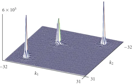
of the 1% of the SPEC’s maximum value are used in simulations. Simulation results, computed at the point (n1T,n2T)=(−0.25,−0.25), are presented inFigure 2. Low
2D SPEC’s concentration, high 2D WD resolution, but with the emphatic cross-terms presence, high quality 2D SM
autoterms’ representation with the only partially suppressed cross-terms, as well as the improved S/SF representation, based on the proposed method, can be noticed from Figures
2(a)–2(d).Figure 2(f)readily proves the pure CTFWD signal representation achieved by the proposed method.
2.3. Noisy Signal Analysis. In practice, signals are always exposed to the additive noise influence. To evaluate noise influence to the proposed method, let us consider the noisy signal x(−→n) = f(−→n) +ε(−→n), where ε(−→n) represents the additive white Gaussian complex noise with variance σ2
ε.
The variance of the real-valued 2D CTFWD estimator (4) is defined by
σxx2
−→ n,−→k
=varCTFWDx
−→ n,−→k
=ECTFWD2x
−→
n,−→k−ECTFWDx
−→
n,−→k2. (6)
It consists of two parts: the signal-and-noise-dependent one, σ2
f ε(−→n,
− →
k), existing only inside regions Di(−→n,−→k), i
= 1,. . .,q, and the noise-only-dependent one, σ2
εε(−→n,
− →
k) existing everywhere (in all frequency-frequency points), σ2
xx(−→n,
−→
k)=σ2
f ε(−→n,
−→
k) +σ2
εε(−→n,
− →
k). Following the procedure from the 1D noisy signal case, [7, 37, 38], after several straightforward transformations, in the case of rectangular lag-window w(−→m), the variance (6) can be derived as
σ2
xx
−→ n,−→k
= ⎧ ⎪ ⎪ ⎪ ⎪ ⎪ ⎪ ⎪ ⎪ ⎨ ⎪ ⎪ ⎪ ⎪ ⎪ ⎪ ⎪ ⎪ ⎩ 2Nσ2 ε − →
L(−→n,−→k)
− →
i=−−→L(−→n,−→k)
SPECf
−→
n,−→k +−→i+σ2
εε
−→ n,−→k,
for−→n,−→k∈Di
−→
n,−→k, i=1,. . .,q,
N2σ4
ε, for
−→
n,−→k∈/Di
−→
n,−→k, i=1,. . .,q, (7)
where σ2
εε(−→n,
−→
k) = N2σ4
ε[
L1(−→n,
− →
k)
i1=1 (L2(
− →n,−→k, +i
1) + L2(−→n,
− →
k,−i1)) +L2(−→n,
− →
k, 0) + 1] andσ2
εε(−→n,
− →
k)=N2σ4
ε outside
regions of supportDi(−→n,
− →
k),i=1,. . .,q(whenL1(−→n,
− →
k)= L2(−→n,
− →
k,±i1)=0).
Note that by performing noisy signal analysis of the proposed method, we have also unified the noisy signal analysis of its special cases (2D SPEC for L1(−→n,
− →
k) = L2(−→n,
− →
k,±i1) = 0, 2D WD for L1(−→n,
− →
k) = L2(−→n,
− →
k,±i1)
= N/2, and 2D SM for L1(−→n,
− →
k) = L2(−→n,
− →
k,±i1) = Lm,
(1) The proposed method minimizes the estimator’s variance σ2
xx(−→n,
− →
k) outside regions Di(−→n,
− →
k), i =
1,. . .,q. Knowing that it also produces the opti-mal autoterms presentation, the proposed method optimizes the peak signal-to-noise ratio in (k1,k2)
points existing outside regions of support. ( The peak signal-to-noise ratio assumes the ratio of the squared peak value of the S/SFD and estimator’s variance σ2
xx(−→n,
−→
k). This is required in many practical appli-cations where the peak values of S/SFD are used to estimate local frequency of an analyzed signal. In this case, we are not interested in the local signal-to-noise ratio, especially in the frequency-frequency points existing outside regions of support (where S/SFDs are equal to zero). In these points, the peak signal-to-noise ratio represents the measure of possible false peak detection (wrong local frequency estimation, [7]).)
(2) The estimator’s variance (7) increases inside regions Di(−→n,−→k),i = 1,. . .,q. However, by taking optimal
number of summation terms in (4), the proposed method decreasesσ2
xx(−→n,
− →
k) and, therefore, improves the peak signal-to-noise ratio regarding the 2D WD and 2D SM in the frequency-frequency points existing inside these regions.
(3) The 2D SPEC minimizes σ2
xx(−→n,
− →
k) in the (k1,k2)
points existing inside regionsDi(−→n,
− →
k),i=1,. . .,q. However, at the same time it produces low signal’s concentration around local frequencies. Therefore, the proposed method can improve 2D SPEC’s estima-tion for the case of highly nonstaestima-tionary 2D signals, even in the regions of support points (k1,k2).
These conclusions have been tested numerically. To this end, signals (5) are exposed to the additive white Gaussian noise with high variance σ2
ε = 1. The same parameters
as in the noiseless case are used here. The considered S/SF representations of the noisy signal are given inFigure 3. They readily prove theoretically derived conclusions. Note that, depending on the noise distribution and the R2selection,
there can exist particular frequency-frequency points outside regions of support in which|STFT(−→n,k1±i1,k2±i2)|2≥R2
and/or|STFT(−→n,k1±i1,k2∓i2)|2≥R2,i1=0,. . .,L1(−→n,
−→
k), i2 = 0,. . .,L2(−→n,
−→
k,−i1), are satisfied. This implies the
nonzero values ofL1(−→n,
−→
k) and/or L2(−→n,
− →
k,−i1) in these
points. However, it does not significantly influence the S/SF representation based on the proposed method, Figures3(d)
and3(e). In line with this conclusion, note that greater values of the reference level R2 (about 5%–10% of the expected
2D SPEC’s maximum value) almost remove these effects,
Figure 3(e).
2.4. Calculation Complexity of the Proposed Method and Comparisons. In this subsection, the proposed method will be compared, regarding the calculation complexity, with the conventional S/SFDs (2D SPEC and 2D WD) and
Table1: Numbers of complex operations by frequency-frequency
point required by the considered S/SFDs. (1) 2D WD (2) calculated
using the FFT routines, (2) 2D SM using the recursive 2D STFT calculation (with 2 complex summations and a complex
multipli-cation, [12]), (3) Proposed method with the 2D STFT calculation
based on the FFT routines, (4) Proposed method using the recursive 2D STFT calculation, whereL2(−→n,−→k)=L1(
−
→n,−→k)
i1=1 (L2(−→n,−→k, +i1) +
L2(−→n,
− →
k,−i1))/2. Multiplications by 2 are not considered, because
the time needed for their execution is much smaller than the time needed for other operations.
S/SFD Additions Multiplications
1 4(log2N+ 1) 2(log2N+ 2)
2 2 +L2
m+Lm L2m+Lm+ 3/2
3
2log2N+L2+
L1(−→n,−→k) +
L2(−→n, − →
k, 0)/2
log2N+L2+
L1(−→n,−→k) +
(L2(−→n, − →
k, 0) + 1)/2
4 2 +L2+L1(
− →n,−→k) +
L2(−→n,−→k, 0)/2
L2+L1(−→n, − →
k) +
L2(−→n,−→k, 0)/2 + 3/2
computationally the simplest reduced interference method (2D SM, see the Introduction). The proposed method based S/SF representation takes variable number of necessary operations (regarding 2D WD autoterms quality) in different frequency-frequency points (k1,k2),k1,k2 =0, 1,. . .,N−1:
the minimal one outside the regions of support (where a great part of these points commonly lie), the higher one inside these regions, and the possible maximum one only in the central points of the widest region (seeFigure 8and the discussion fromSection 5). In this way, the method improves the calculation complexity of the considered S/SFDs for meank1,k2=0,1,...,N−1{L2(−→n,
− →
k) +L1(−→n,
− →
k) +L2(−→n,
− →
k, 0)/2}< 2log2N + 5/2,Table 1. For example, in the analyzed signal (5) case and for Lm = 18, N = 64, average number of
complex operations per frequency-frequency point, required by the proposed method, are 30842/N2 = 7.5 additions
and 28794/N2 = 7 multiplications. Its complexity slightly
differ from the SPEC case (obtained from the proposed method for L1(−→n,
− →
k) = L2(−→n,
− →
k,±i1) = 0), but also
significantly improve calculation complexity of the 2D WD, with 28 complex additions and 16 complex multiplications per frequency-frequency point, and the 2D SM, with 344, 343.5 corresponding operations,Table 1. In addition, among the considered S/SFDs, only the proposed one produces a pure 2D CTFWD signal representation in the practically only important case of multicomponent signals having different autoterms widths,Figure 2. In line with these conclusions, the 2D S/SFD having the same calculation complexity as the proposed method is represented inFigure 2(e). However, it produces only a low concentrated 2D signal representation, very close to the 2D SPEC one.
seriously restrict their applicability. However, hardware implementations (such as the one developed here), when possible, can overcome this drawback, enabling application of these S/SFDs in numerous additional problems in practice.
3. Signal Adaptive Hardware
Implementation Approach
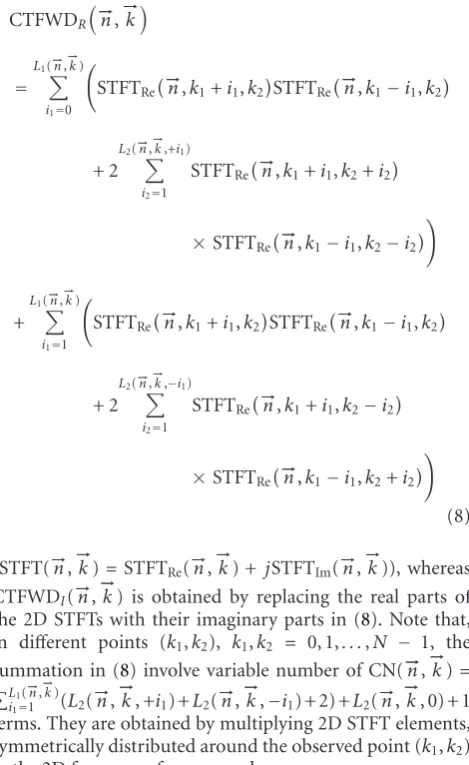
2D CTFWD definition (4) adapted for real time imple-mentation should include only real multiplications. To this end, we express it as a sum of two computational lines, CTFWD(−→n,−→k)=CTFWDR(−→n,−→k) + CTFWDI(−→n,−→k), used
respectively for processing the real and imaginary parts of 2D STFTs (from already available 2D STFT or 2D FFT modules, [20–24, 31]). According to (4), these lines have identical forms. CTFWDR(−→n,
− →
k) is
CTFWDR
−→ n,−→k
=
L1(−→n,−→k)
i1=0
STFTRe
−→
n,k1+i1,k2
STFTRe
−→
n,k1−i1,k2
+ 2
L2(−→n,−→k,+i1)
i2=1
STFTRe
−→
n,k1+i1,k2+i2
×STFTRe
−→
n,k1−i1,k2−i2
+
L1(−→n,−→k)
i1=1
STFTRe
−→
n,k1+i1,k2
STFTRe
−→
n,k1−i1,k2
+ 2
L2(−→n,
− →
k,−i1)
i2=1
STFTRe
−→
n,k1+i1,k2−i2
×STFTRe
−→
n,k1−i1,k2+i2
(8)
(STFT(−→n,−→k)=STFTRe(−→n,
− →
k) +jSTFTIm(−→n,
− →
k)), whereas CTFWDI(−→n,
− →
k) is obtained by replacing the real parts of the 2D STFTs with their imaginary parts in (8). Note that, in different points (k1,k2), k1,k2 = 0, 1,. . .,N − 1, the
summation in (8) involve variable number of CN(−→n,−→k)= L1(−→n,
− →
k)
i1=1 (L2(
−→n,−→k, +i
1) +L2(−→n,
− →
k,−i1) + 2) +L2(−→n,
−→
k, 0) + 1 terms. They are obtained by multiplying 2D STFT elements, symmetrically distributed around the observed point (k1,k2)
in the 2D frequency-frequency plane.
The 2D CTFWD hardware implementation will be pre-sented through the implementation of its real computational line and the control logic, Figures 4 and 5, since the imaginary computational line is identical with the real one, whereas the control units and configuration signals are unique. The design principle follows the developed form of (8), where each summation term is executed during
Table2: Total numbers of complex additions and complex
multi-plications, required by the considered S/SFDs, for differentN. (1)
2D SPEC (the proposed method withL1(−→n,
− →
k)=L2(−→n, − →
k,±i1)=
0), (2) 2D WD calculated using the FFT routines, (3) 2D SM using the recursive 2D STFT calculation, (4) Proposed method using the recursive 2D STFT calculation.
N 1 2 3 4
64 Additions 8192 114688 1409024 30842
Multiplications 6144 65536 1406976 28794
128 Additions 32768 524288 5636096 86477
Multiplications 24576 294912 5627904 78285
256 Additions 131072 2359296 22544384 230630
Multiplications 98304 1310720 22511616 197860
512 Additions 524288 10485760 90177536 578450
Multiplications 393216 5767168 90046464 447380
the corresponding step which takes one CLK cycle. In this way, we are able to balance the amount of work done in each CLK, resulting in minimization of the CLK cycle time. During the first CLK, when −→L(−→n,−→k) = −→0 , the 2D SPEC is calculated from the 2D STFT element, STFT(−→n,−→k), situated in the central point of the convolution window, Figure 6(a). Residual summation terms, obtained for the increased indexesi1 and/or i2 in subsequent CLKs
(second, third,. . .) and existing only in regions of support frequency-frequency points, are the conditional ones. They are used to improve the S/SFD concentration with the goal to achieve the 2D WD one. Therefore, the 2D CTFWD real time implementation requires variable number of CLKs by frequency-frequency point (i.e., by one convolution window position) to be executed, where only 2D SPEC execution CLK (the first one) remains the unconditional one in each point (k1,k2),k1,k2=0, 1,. . .,N−1.
In general, each 2D CTFWD element is produced by sliding 2D convolution window over the 2D STFT input elements and by computing the 2D CTFWD output value according to the input elements and the algorithm (8). The obtained result is a 2D CTFWD element assigned to the center of the 2D convolution window, Figure 6(a). Following these observations, the architecture for real time design of the 2D CTFWD real computational line consists of several main functional units, Figure 4. The STFT-to-CTFWD gateway, Figure 5, represents a functional kernel of the proposed architecture. It is used to produce 2D CTFWD outputs based on the 2D STFT input elements obtained from the convolution window register block. The (2Lm+ 1)×(2Lm + 1) convolution window register block
and 2Lmfirst-in-first-out (FIFO) delays mutually implement
the 2D convolution window function, presented in detail in
31 k1
−32
31 k2
−32
1×10⁴
(a)
6×10⁵
(b)
6×10⁵
(c)
6×10⁵
(d)
8×10⁴
(e)
6×10⁵
(f)
Figure2: S/SF representations of signal (5): (a) 2D SPEC, (b) 2D WD, (c) 2D SM corresponding to the widest signal component, (d)
Proposed method based representation, (e) S/SF representation having the same calculation complexity as the proposed method, (f)
Difference between graphics (b), (d).
The operation principle can be described as follows.
(1) The STFT IN elements are imported to the input memory owing to each double CLK cycle, corresponding to the minimal execution time required by a frequency-frequency point (2D SPEC execution time). This period simultaneously determines sampling rate of the analyzed analogue 2D signal. By eachSTFT Loadcycle, an STFT IN element is moved from the input memory to the convolution window area that is sliced over input 2D STFTs for one position right, as shown inFigure 6.
1×10⁴
31 k1
−32
31
k2
−32
(a)
6×10⁵
(b)
6×10⁵
(c)
6×10⁵
(d)
6×10⁵
(e)
Figure3: S/SFDs of noisy signal (5): (a) 2D SPEC, (b) 2D WD, (c) 2D SM corresponding to the widest signal component, (d), (e) proposed
method based S/SFDs corresponding toR2of 1% and 5% of the expected 2D SPEC’s maximum value.
(in different frequency-frequency points) and CN(−→n,−→k) + 1 times greater than the CLK period.
(3) In the corresponding CLKs, signals x±i1,±i2 and x±i1,∓i2 are generated as: x±i1,±i2 = 1 if
|STFT(−→n,k1±i1,k2±i2)|2 > R2 andx±i1,±i2 =0 otherwise, that is, x±i1,∓i2 = 1 if |STFT(
− →n,k
1±i1,k2∓i2)|2 > R2
and x±i1,∓i2 = 0 otherwise. They, respectively, determine nonzero values of STFT(−→n,k1 ± i1,k2 ± i2) and of
STFT(−→n,k1±i1,k2∓i2),i1=0, 1,. . .,L1(−→n,
−→
k),i2=0, 1,. . .,
L2(−→n,
− →
k,±i1) and simultaneously produce the RegionSup
control signal, RegionSup = xi1,±i2 · x−i1,∓i2. Zero value of the RegionSup signal implies following actions: (1) Through the participation in the CumADD CLK signal generation, disables the corresponding term, non-existing inside the regions of support domains, to enter the summation (8), and (2) Through the participation in the
RESET L and the High Count CLK signals generation, terminates the summation in +i2 and in −i2 (for each
i1, i1 = 0, 1,. . .,L1(−→n,
− →
STFT IN Input memory
2
×
CLK
(2Lm+ 1)×(2Lm+ 1) convolution window register block (k1+Lm,k2+Lm) (k1+lm,k2) (k1+lm,k2−Lm)
(k1,k2+Lm) (k1,k2) (k1,k2−Lm)
(k1−Lm,k2+Lm) (k1−Lm,k2) (k1−Lm,k2−Lm)
FIFO delay (N−(2Lm+ 1))
FIFO delay (N−(2Lm+ 1)) FD FD
Ctrl of windowed convolution
and padding borders STFT-to-CTFWD gateway
CTFWD OUT FIFO delay (FD)
Start convolution (SC) Max. con. win. width (MCWW)
Down border (DB) End of process (EOP) Din
Address Enable (EN)
Configuration registers CLK STFT Load
Start Process Left Border Down Border End Proc SC
MCWW DB EOP
Figure4: Proposed signal adaptive hardware design. In registers, the S/SF position of the stored 2D STFT element is denoted.
Completion RS
Completion Cond CLK
High count outputs Low count outputs RegionSup SHLorNo Termination Ctrl of execution
STFT Load/CTFWD Store RESET/CumADD clear CumADD CLK SPEC EN RESET L High count CLK CLK
inv(CLK) D Q
Con
fi
gu
ra
ti
on
sig
n
als
(fr
o
m
P
C
o
r
M
C)
RESET High count CLK RESETL
High bin count
Low bin count
System CLK
Main ctrl
LU
T
A
d
d
LUT (RAM
or ROM)
Completion SelSTFT 1 SelSTFT 2 SHLorNo Completion Cond Terminaton Inputs from convolution
window register block
MUX1
MUX2 SelSTFT 1
SelSTFT 2
Real (Re) computational line of STFT-to-CTFWD gateway ShLeft CumADD
SHLorNo CumADD CLK CumADD clear
OutREG
CTFWD Store
STFTRe(−→n,k1+i1,k2±i2) STFTIm(−→n,k1+i1,k2±i2)
Ctrl of the region of support determination ADD
R2 Left Border Bottom Border
COMP xi1,±i2 x−i1,∓i2
RegionSup D flip-flop
D Q RS
CLK +
+
Algorithm (8)
N/2−1 N/2−1 2D CTFWD
−N/2
k1 k2
−N/2
2D convolution window
Path of convolution window
2D STFT
2Lm+ 1 Lm
−N/2
N/2−1 k1 k2
N/2−1
−N/2
Lm 2 Lm +1 · · · · · · · · · · · · · · · · · · · · · · · · · · · . . . . . . . . . . . . . . . . . . . . . . . . . . . · · ·... · · · · · · · · · · · · . . . . . . . . . . . . . . . . . . . . . . . . . . . · · ·... (a)
(k1−Lm,k2−N/2)
(k1 ,k2−N/2)
(k1 +Lm,k2−N/2)
(k1−Lm,k2−Lm)
(k1 ,k2−Lm)
(k1 +Lm,k2−Lm)
(k1−Lm,k2 )
(k1 ,k2 )
(k1 +Lm,k2 )
(k1−Lm,k2 +Lm)
(k1 ,k2 +Lm)
(k1 +Lm,k2 +Lm)
(k1−Lm,k2 +Lm+ 1)
(k1 ,k2 +Lm+ 1)
(k1 +Lm,k2 +Lm+ 1)
(k1−Lm,k2 +N/2−1)
(k1 ,k2 +N/2−1)
(k1 +Lm,k2 +N/2−1) · · · · · · · · · · · · · · · · · · · · · · · · · · · · · · · · · · · · . . . . . . . . . . . . . . . . . . . . . . . . . . . . . . . . . . . . (b)
(k1−Lm,k2−N/2)
(k1−Lm+ 1,k2−N/2)
(k1 ,k2−N/2)
(k1 +Lm,k2−N/2)
(k1 +Lm+ 1,k2−N/2)
(k1−Lm,k2−N/2 + 2Lm)
(k1−Lm+ 1,k2−N/2 + 2Lm)
(k1 ,k2−N/2 + 2Lm)
(k1 +Lm,k2−N/2 + 2Lm)
(k1 +Lm+ 1,k2−N/2 + 2Lm)
(k1−Lm,k2 )
(k1−Lm+ 1,k2 )
(k1 ,k2 )
(k1 +Lm,k2 )
(k1 +Lm+ 1,k2 )
(k1−Lm,k2 +N/2−2Lm−1)
(k1−Lm+ 1,k2 +N/2−2Lm−1)
(k1 ,k2 +N/2−2Lm−1)
(k1 +Lm,k2 +N/2−2Lm−1)
(k1 +Lm+ 1,k2 +N/2−2Lm−1)
(k1−Lm,k2 +N/2−1)
(k1−Lm+ 1,k2 +N/2−1)
(k1 ,k2 +N/2−1)
(k1 +Lm,k2 +N/2−1)
(k1 +Lm+ 1,k2 +N/2−1) · · · · · · · · · · · · · · · · · · · · · · · · · · · · · · · · · · · · · · · · · · · · · · · · · · · · · · · · · · · · . . . . . . . . . . . . . . . . . . . . . . . . . . . . . . (c)
(k1 +Lm,k2 +Lm)
(k1 ,k2 +Lm)
(k1−Lm,k2 +Lm)
(k1 +Lm,k2 )
(k1 ,k2 )
(k1−Lm,k2 )
(k1 +Lm,k2−Lm)
(k1 ,k2−Lm)
(k1−Lm,k2−Lm)
(k1 +lm,k2−Lm−1) (k1 +Lm,k2−N/2) (k1 +Lm−1,k2 +N/2−1) (k1 +Lm−1,k2 +Lm+ 1)
(k1 ,k2−Lm−1) (k1 ,k2−N/2) (k1 + 1,k2 +N/2−1) (k1 + 1,k2 +Lm+ 1)
(k1−Lm+ 1,k2−Lm−1) (k1−Lm+ 1,k2−N/2) (k1−Lm,k2 +N/2−1) (k1−Lm,k2 +Lm+ 1)
· · · · · · · · · · · · · · · · · · · · · · · · · · · · · · · · · · · · · · · · · · · · · · · · · · · · · · . . . . . . . . . . . . . . . . . . . . . . . .
2D STFT elements-inputs of the STFT-to-CTFWD getaway
2LmFIFO delays N−(2Lm+ 1) (2Lm+ 1)×(2Lm+ 1) convolution window register block
STFT
(
−→ n, k1 + Lm , k2 + Lm +1 ) (d)
Figure 6: (a) Procedure of 2D convolution window sliding and of 2D CTFWD producing; (b) Actual convolution window position
corresponding to the point (k1,k2) (thick solid line) and its next position (thick dashed line); (c) Actual convolution window position
−i2 and for the next i1, respectively. Further, zero value
of the RegionSup signal, reached in the CLK cycle when
SHLorNo=0 (corresponding to the first zero summation term from (8) not multiplied by 2), terminates the summation (8) ini1, resulting in the calculation completion
(in the next CLK) for the observed point (k1,k2). In that
line, the RS signal, RS=inv(RegionSup), participates in the
STFT Load/CTFWD Store, CumADD clear/RESET signals generation. With a latency of half of a CLK, the system is reset and the execution for the next frequency-frequency point begins. In this way, the RegionSup signal allows the proposed design to optimize the number of CLKs taken in different frequency-frequency points within the execution. The SPEC EN signal provides execution of the unconditional (2D SPEC execution) cycle, even ifx0,0=0.
A look-up table memory (LUT), Table 3, manages the execution. Its locations consist of the 4-bit control signals area and MUX addresses. Functions of generated control signals are given inTable 4. Binary counter Low Bin Count generates LUT’s low addresses, controlling the summation (8) in +i2and in−i2. Binary counter High Bin Count sets
LUT’s high addresses, controlling the summation (8) ini1.
Operations at the bordering positions, as well as the whole S/SF process, are managed by theStart Process,Left Border,
Bottom BorderandEnd Processsignals,Table 4. These signals are generated by considering input parameters from the Configuration registers,Table 5, as well as the synchroniza-tion condisynchroniza-tions related to the CLK and STFT Load cycles. They are produced in the modules that consist of variable length up-down binary counters and binary magnitude comparators whose binary references are parameters from the Configuration registers.
The longest path that determines the fastest CLK cycle time corresponds to the generation of theRegionSupsignal in a half of a cycle, through a multiplier, an adder and a com-parator (Tc/2=Tm+Ta+Tcomp, whereTc,Tm,Ta,Tcompare
CLK cycle, multiplication, addition, and comparison times, resp.). In this way, we enable participation of theRegionSup
signal in theCumADD CLKsignal generation in the second half of the same CLK (see timing diagram from Figure 8). Maximum output register lengths for each used digital unit are given inTable 6. They are derived as functions of the 2D STFT data length (l), maximum convolution window width (Lm) and the number of frequency points (N). Note that
critical point is the width of the CumADD/OutREG. The longest path depends on the 2D STFT data length only.
4. Testing and Verification of
the Proposed Design
The proposed system for S/SF analysis has been verified with an FPGA device real time design. The FPGA implementation approach is chosen in line with the fact that recently high performance devices for solving practical problems in signal processing tend to be implemented in an FPGA, instead of in a DSP, chip. This is possible because the gate densities available in FPGAs now allow fairly sophisticated DSP algorithms to be implemented within a single chip, [39,40].
31 k1
−32
31 k2
−32
6×10⁵
Figure 7: S/SF representation of the analyzed signal (5) in
(n1T,n2T) = (−0.25,−0.25), obtained by using the proposed
hardware design withLm=5, implemented in FPGA device.
Additionally, languages used for the hardware description of FPGA chips provide a high level behavioral design methodology, requiring high flexibility from the targeted device, so that the synthesis tool will be able to produce both efficient device utilization and high performance. Also, usage of recent FPGA chips with huge internal memory blocks is considered to be a powerful tool for implementation of convolution and delay operators that are of essential importance in implementation of DSP algorithms.
Hardware realization of the proposed system withLm =
5 is performed by using the EP2S15F672C5 device from the Stratix II family. Rates of utilization of device’s silicon resources are given in Table 7. Before programming the selected FPGA device, the compilation and simulation have been performed by processing the test signal (5). The 2D STFT elements (their real and imaginary parts), numerically computed inSection 2, normalized to the range [0 255], and rounded to the 8-bit integers, are imported to the designed system input. Results of the real time implementation are presented inFigure 7. Accuracy of these results can easily be checked by comparison with the numerical results given in
Figure 2(d). Also, the obtained results can be readily proven by analyzing simulation results given inFigure 8. In line with the simulation results analysis, note that the developed signal adaptive system withLm =5 requires convolution window
register blocks (for storing the real and imaginary parts of the input 2D STFT elements) of (2Lm + 1)×(2Lm+ 1) =
121 parallel-in-parallel-out registers. However, presentation of the content of all these registers in a single figure is impossible. Therefore, in Figure 8 we present contents of the central registers and their neighborhood registers, named in line with their relative position with respect to the central ones. For example, in the first marked instant, corresponding to the outside regions of support frequency-frequency point, CTFWD OUT=2D SPEC=(−3)2+ 92=
90 has been derived from (8) in two CLKs, since x0,0 =0
(32+ 92 = 90 < R2 =94). Note that multiplication and
shift operations are parallel, while adding has a latency of half of a CLK. In the second marked instant, corresponding to the marginal frequency-frequency point from the detected region of support, CTFWD OUT=12+ (−11)2=
Table3: Content of LUT memory locations for givenLm. ADDM,Mdenotes address of central element of the convolution window register
block, symboldenotes shift left logical operation andr=Length(SelSTFT 1). Control signals area contains following bits: (1)SHLorNo,
(2)Completion Cond, (3)Termination, (4)Completion.
Address Ctrl Signals Area
SelSTFT 1 SelSTFT 2
High Low 1 2 3 4
0 0 0 0 0 0 ADDM,Mr ADDM,M
0 1 1 1 0 0 ADDM,M+1r ADDM,M−1
..
. ... 1 0 0 0 ... ...
0 Lm 1 0 1 0 ADDM,M+Lmr ADDM,M−Lm
1 0 0 0 0 0 ADDM+1,Mr ADDM−1,M
1 1 1 1 0 0 ADDM+1,M+1r ADDM−1,M−1
..
. ... 1 0 0 0 ... ...
1 Lm 1 0 1 0 ADDM+1,M+Lmr ADDM−1,M−Lm
2 0 0 0 0 0 ADDM+1,Mr ADDM−1,M
2 1 1 1 0 0 ADDM+1,M−1r ADDM−1,M+1
..
. ... 1 0 0 0 ... ...
2 Lm 1 0 1 0 ADDM+1,M−Lmr ADDM−1,M+Lm
..
. ... ... ... ... ... ... ...
2Lm−1 0 0 0 0 0 ADDM+Lm,Mr ADDM−Lm,M
2Lm−1 1 1 1 0 0 ADDM+Lm,M+1r ADDM−Lm,M−1
..
. ... 1 0 0 0 ... ...
2Lm−1 Lm 1 0 1 0 ADDM+Lm,M+Lm r ADDM−Lm,M−Lm
2Lm 0 0 0 0 0 ADDM+Lm,Mr ADDM−Lm,M
2Lm 1 1 1 0 0 ADDM+Lm,M−1r ADDM−Lm,M+1
..
. ... 1 0 0 0 ... ...
2Lm Lm 1 0 1 0 ADDM+Lm,M−Lmr ADDM−Lm,M+Lm
2Lm+ 1 0 0 0 0 1 0 0
Table4: Function of control signals generated by the Main Ctrl and the ctrl of windowed convolution and padding borders.
Control signal Effect
SelSTFT1,2
Enable sharing of the STFT-to-CTFWD gateway for different 2D STFT inputs in different CLKs within the
execution in the observed frequency-frequency point
SHLorNo Provides multiplication by 2 of the partial product term according to (8)
Completion Cond Allows theRSsignal to produce the completion CLK from the conditional one
Termination&
Completion
Provide termination of the summation (8) in +i2and in−i2and its completion, respectively, in
frequency-frequency points in which theRegionSupsignal cannot achieve zero value and, therefore, cannot
assume the role described in the operation principle 3. ( In practical implementations, the relatively smallLm
values, 5≤Lm≤7, are usually applied. They provide the desired—2D WD—concentration (compare the
representation fromFigure 2(d), obtained forLm=18, with the representation fromFigure 6, obtained for
Lm=5), but also significantly simplify hardware implementation (seeTable 8). However, a predefined
maximum convolution window width corresponding to theseLmvalues can be smaller than the theoretically
required one in the points (k1,k2) existing around the local frequency. Therefore, in these points, theRegionSup
signal cannot achieve zero value, needed for the termination of the summation (8) in +i2and in−i2and its
completion, according to the principle 3 of the hardware operation.)
Left Border&
Bottom Border
Through the participation in theRegionSupsignal generation, allow padding the left and bottom borders with
Table5: Parameters from configuration registers, expressed by the number of neededSTFT Loadcycles.
Configuration register Parameter specified and its description Parameter’s value
Start Convolution (SC) Start of the convolution window operation LmN+Lm
FIFO Delay (FD) Delay for generating data in row’s time index N−(2Lm+ 1)
Conv. Win. Size (CWS) Size of convolution window 2Lm+ 1
Bottom Border (BB) Bottom border position N×(N−1)
End of Frame (EOF) End of frame position N×N−1
Table6: Output registers lengths for used digital units depending on the parametersl,Lm, andN.
Length of MUXs MULTs ADD ShLeft CumADD, OutREG
Parametersl,Lm,N l 2·l CEIL(log2(2·(22l−1))) 2·l+ 1 CEIL(log2((22l+1−1)×(2L2m+ 3Lm+ 1)))
Table7: Summarized resource utilization for real device andLm=5,N=64 and 2D STFT data lengthl=8.
Chip Family Recommended Device Logic utilization Combinational ALUTs Dedicated logic registers Total registers
Stratix II EP2S15F672C5 19% 1,027/12,480 (8%) 1,905/12,480 (15%) 1905
Total I/O Total virtual Total block memory DSP block 9-bit Total Total
Pins used pins used bits used elements PLLs DLLs
345/367 (94%) 0 75,066/419,328 (18%) 2/96 (2%) 0/6 (0%) 0/2 (0%)
Table8: Hardware complexity of the considered implementations of 2D systems.
Implementation No. of used functional units No. of memory locations
No. of adders No. of multipliers No. of shift left reg.
Parallel (when it is possible) 4L2
m+ 4Lm+ 1 4L2m+ 4Lm+ 2 4L2m+ 4Lm 4NLm+ 4Lm+ 8
MCI with a fixed number of CLKs 3 2 2 4NLm+ 2L2m+ 6Lm+ 10
Proposed signal adaptive 5 6 2 2N2+ 4NL
m+ 2L2m+ 8Lm+ 10
Table9: CLK cycle times and execution times (by frequency-frequency point) of the considered implementations of 2D systems.TcP,TcSF,
TcSAare CLK cycle times in the cases of the parallel design, MCI one with a fixed number of CLKs and the signal adaptive one, respectively,
whereasTsis the 1-bit shift time. Execution time of the proposed design has been calculated for the considered signal (5) andN=64,Lm
=5. Total number of CLKs taken by the proposed design is 35326, whereas the average number of CLKs by frequency-frequency point is
35326/642=8.6245.
Implementation Clock cycle time Execution time
Parallel (when it is possible) TcP=2Tm+ (2L2m+ 2Lm+ 2)Ta+Ts TcP
Serial with a fixed number of CLKs TcSF=Tm+ 2Ta+Ts (2L2m+ 2Lm+ 2)TcSF
Proposed signal adaptive TcSA=2Tm+ 2Ta+ 2Tcomp 8.6245×TcSA
been derived from (8) in four CLKs, sincex0,−1=0 ((−3)2+92
=90< R2=94) andx
−1,0=0 (12+ 12=2< R2=94). In the
third marked instant, corresponding to the region of support frequency-frequency point, CTFWD OUT=(−10)2+ 102+ 2×(10×1 + (−10)×(−11))=440 has been derived from (8) in five CLKs, sincex0,−2=0 ((−3)2+ 92=90< R2=94)
andx−1,0=0 (12+ 12 =2 < R2=94). Variable number of
CLKs, taken by the proposed design in different frequency-frequency points, can easily be observed by considering the period of theSTFT Loadcycle, or the period of the RESET
cycle inFigure 8. Illustration of the number of taken CLKs in the corresponding frequency-frequency points is given by the gray-scale shaded graph inFigure 9.
5. Comparative Analysis
CLK RS RegionSup STFT Load RESET CumADD CLK Reg Cent Re Reg Cent Im Reg Left1 Re Reg Left1 Im Reg Right1 Re Reg Right1 Im Reg left2 Re Reg Left2 Im Reg Right2 Re Reg Right2 Im Reg Up1 Re Reg Up1 Im Reg Dwn1 Re Reg Dwn1 Im CTFWD OUT Name
3.45 ms 3.451 ms 3.452 ms 3.453 ms +3.451708031 ms +3.45229925 ms +3.45310864 ms
0 0
−12 8
0 0
0 0
9 −11
9 −11
0 0
0 9 −11
−3 9
−3 9 0 0
0 0
9 −11 −3
9
1 −11
1 −11
−3 9 1 −11
9 −11 −10 10
−10 10
202
1 −11 −10 10 −3 9 10 −10 9 −11
10 −10
90
−10 10 10 −10
1 −11
−1 11 −3 9 −1 11
122 1 1
10 −10 −1 11 −10 10 2 −10
1 −11
2 −10
440
Figure8: Illustration of the simulation results around the frequency-frequency instant when the region of support is detected.
−32
k2
31
−32
k1
31
Figure 9: Illustration of the number of CLKs taken by the proposed design in corresponding frequency-frequency points during the
execution. Different numbers of CLKs are illustrated by gray-scale shaded points, where the white ones denote minimal number of 2 CLKs,
whereas the black ones denote maximum number of 2L2
m+ 3Lm+ 2=67 CLKs.
[33], and the existing MCI one with a fixed number of CLKs, [34]. Trade-offs and comparisons of the considered implementation approaches are summarized in Tables8and
9. In general, MCI designs imply both minimal hardware requirements and much shorter CLK cycle time in com-parison to the parallel design. Note that the minimal total number of used memory locations in parallel design is the consequence of the LUT memory absence in this case (i.e., absence of LUTs of 2L2
m + 3Lm + 2 locations and of
2L2
m+ 2Lm+ 2 locations in the cases of the proposed signal
adaptive design, Table 3, and the MCI design with a fixed number of CLKs, [34], resp.). Also, the proposed signal adaptive design includes two input memories, capacity of maximum N2 locations, used to store real and imaginary
parts of input 2D STFT elements and to allow importing (in process) of these elements with a variable (STFT Load) cycle. Input memories additionally allow the fastest possible sampling interval of the analyzed analogue 2D signal in all considered implementation cases. However, observe that the total number of used memory locations remains quite small in all these cases.
part of total frequency-frequency points commonly lie), the higher one inside these regions, and the possible maximum one only around the central points of each region of support, Figure 9. In this way, the proposed design can significantly improve the execution time with respect to the other designs, removing the main drawback of the MCI architectures in comparison to the parallel ones, [34]. For example, in the analyzed signal (5) case, when Lm =5,N
=64 are applied, the proposed design improves execution time in comparison to the other corresponding designs for Ts,Tcomp Tm < 2.935×Ta, Table 9. Finally, only
the proposed design produces a pure 2D CTFWD signal representation, optimizing both the calculation complexity and the noise influence suppression. Non-adaptive systems cannot produce so high S/SF representation quality, Figures
2,3, and6.
In accordance with the design principle considered here, the number of CLKs taken in different frequency-frequency points corresponds to the number of real summation terms (or to the number of real multiplications) in (8) incremented for the completion CLK and, in some cases (region of sup-port points that include non-maximum number of summa-tions), for some termination CLKs. Therefore,Figure 9can simultaneously approximate the distribution of the number of necessary operations taken by frequency-frequency point. In line with this notation, observe that, in this case, white shaded frequency-frequency points correspond to 2 complex additions (used in the recursive 2D STFT calculation, [12], since 2D SPEC calculation includes only one summation term and does not include summation execution) and 3/2 complex multiplications (2 real multiplications-used, according to (8), in real and in imaginary computational line-corresponding to a half of a complex multiplication and a complex multiplication for the recursive 2D STFT calculation, [12]). In addition, note that this observation is in a full correspondence with theoretical analysis, summarized inTable 1.
6. Conclusion
Signal adaptive multiple-clock-cycle hardware design for S/SF signal analysis has been developed, based on the 2D method for improved S/SF signal representation, also proposed here. The proposed design optimizes critical design performances, related to hardware complexity, making it possible to perform S/SF analysis by using standard devices like FPGA. Allowing the developed 2D system to take a variable number of CLKs in different frequency-frequency points, the signal adaptive design optimizes the execution time, significantly improving it in comparison to the other designs (the parallel one and the existing MCI one with a fixed number of CLKs). In this way, the design simul-taneously produces the optimal—2D WD—presentation of autoterms, as well as the pure cross-terms-free S/SF signal representation in the practically only important case of the nonstationary multicomponent signals having different widths of autoterms.
References
[1] L. Cohen, Time-Frequency Analysis, Prentice-Hall, Upper
Saddle River, NJ, USA, 1995.
[2] W. J. Pielemeier, G. H. Wakefield, and M. H. Simoni,
“Time-frequency analysis of musical signals,”Proceedings of the IEEE,
vol. 84, no. 9, pp. 1216–1230, 1996.
[3] F. Hlawatsch and G. F. Boudreaux-Bartels, “Linear and
quadratic time-frequency signal representations,”IEEE Signal
Processing Magazine, vol. 9, no. 2, pp. 21–67, 1992.
[4] J. Jeong and W. J. Williams, “Kernel design for reduced
inter-ference distributions,”IEEE Transactions on Signal Processing,
vol. 40, no. 2, pp. 402–412, 1992.
[5] LJ. Stankovi´c, “A method for time-frequency analysis,”IEEE
Transactions on Signal Processing, vol. 42, pp. 225–229, 1994. [6] LJ. Stankovi´c, “Multitime definition of the Wigner higher
order distribution: L-Wigner distribution,”IEEE Signal
Pro-cessing Letters, vol. 1, no. 7, pp. 106–109, 1994.
[7] LJ. Stankovi´c, V. Ivanovi´c, and Z. Petrovi´c, “Unified approach to noise analysis in the Wigner distribution and spectrogram,”
Annales des T´el´ecommunications, vol. 51, no. 11-12, pp. 585– 594, 1996.
[8] D. E. Dudgeon and R. M. Mersereau,Multidimensional Digital
Signal Processing, Prentice-Hall, Upper Saddle River, NJ, USA, 1984.
[9] J. W. Woods, Multidimensional Signal, Image and Video
Processing and Coding, Elsevier, Amsterdam, The Netherlands, 2006.
[10] L. D. Jacobson and H. Wechsler, “Joint
spatial/spatial-frequ-ency representation,”Signal Processing, vol. 14, no. 1, pp. 37–
68, 1988.
[11] A. Jakobsson, S. L. Marple Jr., and P. Stoica, “Computationally
efficient two-dimensional capon spectrum analysis,” IEEE
Transactions on Signal Processing, vol. 48, no. 9, pp. 2651–2661, 2000.
[12] S. Stankovi´c, LJ. Stankovi´c, and Z. Uskokovi´c, “On the local frequency, group shift, and cross-terms in some mul-tidimensional time-frequency distributions: a method for
multidimensional time-frequency analysis,”IEEE Transactions
on Signal Processing, vol. 43, no. 7, pp. 1719–1724, 1995. [13] Y. M. Zhu, F. Peyrin, and R. Goutte, “Transformation de
wigner-ville: description d’un nouvel outil de traitement du
signal et des images,”Annales des T´el´ecommunication, vol. 42,
no. 3-4, pp. 105–118, 1987.
[14] Y. M. Zhu, R. Goutte, and M. Amiel, “On the use of two-dimensional Wigner-Ville distribution for texture
segmenta-tion,”Signal Processing, vol. 30, no. 3, pp. 329–353, 1993.
[15] G. Cristobal, C. Gonzalo, and J. Bescos, “Image filtering and analysis through the Wigner distribution function,” in
Advances in Electronics and Electron Phisics, P. W. Haekes, Ed., Academic Press, Boston, Mass, USA, 1991.
[16] J. Hormigo and G. Cristobal, “High resolution spectral
analysis of images using the pseudo-wigner distribution,”IEEE
Transactions on Signal Processing, vol. 46, no. 6, pp. 1757–1763, 1998.
[17] S. R. DeGraaf, “SAR imaging via modern 2-D spectral
estimation methods,”IEEE Transactions on Image Processing,
vol. 7, no. 5, pp. 729–761, 1998.
[18] LJ. Stankovi´c, S. Stankovi´c, and I. Djurovi´c,
“Space/spatial-frequency analysis based filtering,”IEEE Transactions on Signal