ABSTRACT
LAL, DEEKSHA. High-Performance Analog-to-Digital Interfaces in Advanced SiGe BiCMOS Processes for Millimeter-Wave Applications. (Under the direction of Dr. David S. Ricketts.)
Emerging communication technologies of the near future are being enabled by the frequencies at or near the millimeter-wave (mmWave) spectrum (30-300GHz), which provides faster data rates. For very high performance wired and wireless applications in mmWave, such as digital phased arrays, 100GbE and 400GbE Ethernet, and RF Sampling oscilloscopes, several challenges still exist in meeting the diverse dynamic range, bandwidth and integration needs. This work investigates the ability of advanced SiGe BiCMOS technologies to address these challenges, especially in the Analog-to-Digital Converter (ADC) block - which is the common denominator for the digital signal processing used in these applications. Over the past decades, ADC design has shifted away from BiCMOS processes, due to the high integration and digital calibration capabilities of scaled CMOS technologies. However, advanced BiCMOS processes, especially the 90nm SiGe BiCMOS process from GlobalFoundries, show promise for the design of multi-GS/s ADCs, with the combined benefit of high fT npn HBTs that have high intrinsic gain, and the digital integration possible from the 90nm CMOS available in this process.
The objective of this research is to push the performance limits for ADCs for mmWave applications using Silicon-Germanium (SiGe) Heterojunction Bipolar Transistors (HBTs). High performance receivers for these applications must have low cost, low power, small form factor, high sampling rate, medium to high resolution and a wide input bandwidth. The scope of this work is to first determine the design bottlenecks in ADCs through system level VerilogA and Simulink modeling, and then optimize and integrate circuit level designs of those bottlenecks to design front-ends for analog-to-digital blocks. The research includes the design of high speed sampling Track and Hold Amplifiers, Analog to Digital Converters, and one section focusses on BiCMOS mmWave mixers.
from low device intrinsic gain. It is proposed that ADCs implemented in BiCMOS have the potential to change these trends, through performance improvements that lower the calibration requirements for GS/s TI ADCs, and leverage the high performance npn HBTs available. The review is used to identify the Pipelined ADC as a potential candidate for investigating this research. The aim is to develop techniques and methodologies necessary to achieve these goal, and examine the benefits and limitations BiCMOS processes may present to linearity and bandwidth improvements in TI ADCs.
A detailed analysis and illustration of the functioning and operation of a 1GS/s RF sampling Pipelined ADC, as published in [ADB+14], is performed, through system
modeling in VerilogA. It is demonstrated that the BiCMOS designs of the three major blocks of a pipelined ADC - the comparators for the Flash sub-ADC, the sampling network, and the OTA - are comparable in performance in speed and power to the CMOS designs published in [ADB+14], and that the design of multi-GS/s high performance pipelined
ADCs in BiCMOS has substantial potential. This sets the stage for further analysis of these blocks in di↵erent technologies. The dual-rank sampling stages for TI ADCs are investigated due to their front-end linearity and bandwidth limiting performance. The front-end sampling network for multi-GS/s ADCs is chosen as critical to their overall noise and linearity performance, and through an analysis of prior state-of-the-art sampler designs, the designs, architectures, and performance trade-o↵s for their implementations are compared and contrasted, particularly for Switched-Capacitor and Switched Emitter Follower designs in advanced CMOS and BiCMOS processes.
for a 90nm BiCMOS sampler than a 28nm sampler, while 28nm CMOS switches are faster for the sampling aspect [LAR18].
The last part of this research performs an investigation of the linearization technique using a replica capacitor for high speed sampling bu↵ers. This includes provision of a small-signal and large-signal explanation for its functioning and linearization e↵ects, and the presentation of a design methodology for designing samplers using this technique across three di↵erent processes - a 90nm BiCMOS process, a 28nm CMOS process, and a 45nm PDSOI process. A new explanation for the linearization e↵ect by the replica capacitor is presented, by delineating the HD3 from the follower device and the common-gate device. Finally, a methodology for the design of these bu↵ers across the three di↵erent processes is provided.
A final contribution is from the demonstration of a state-of-the-art 140-160GHz dual-sideband mixer, as shown in Appendix A, and published in the 2016 European Microwave Conference [LAR16]. A comparison with prior art in SiGe receivers in similar frequency ranges demonstrates this work to have the widest 3dB IF and RF bandwidths, and a compact footprint of 0.33mm2. The measured 3dB RF bandwidth extends beyond 30GHz,
©Copyright 2019 by Deeksha Lal
High-Performance Analog-to-Digital Interfaces in Advanced SiGe BiCMOS Processes for Millimeter-Wave Applications
by Deeksha Lal
A dissertation submitted to the Graduate Faculty of North Carolina State University
in partial fulfillment of the requirements for the Degree of
Doctor of Philosophy
Electrical Engineering
Raleigh, North Carolina
2019
APPROVED BY:
Dr. David S. Ricketts Dr. Brian A. Floyd
Chair of Advisory Committee
Dr. Paul D. Franzon Dr. Chih-Hao Chang
Technical Consultant:
DEDICATION
To everyone who fed and nurtured my bookconsuming tendencies
-There is no Frigate like a Book To take us Lands away Nor any Coursers like a Page
Of prancing Poetry — This Traverse may the poorest take
Without oppress of Toll — How frugal is the Chariot That bears the Human Soul —
BIOGRAPHY
Deeksha Lal was born and raised in Delhi, India. She received her Bachelors in Engineering degree (First Class with Distinction) in Electrical Engineering from Delhi College of Engineering, Delhi, India in 2013.
In Fall 2013, she joined the PhD program in the Electrical and Computer Engineering Department at North Carolina State University. As a Research Assistant with Dr. David Ricketts, her work focussed on high-performance sampler front-ends for ADCs, and design of mmWave mixers. In the summers of 2015 and 2016, she was an intern with the High Speed Converters group at Analog Devices Inc., Greensboro, NC, where she continued research on samplers for GS/s ADCs, under the mentorship of Dr. Ahmed M. A. Ali.
ACKNOWLEDGEMENTS
Doctoral degrees are made possible by standing, and staying, on the shoulders of giants. It took me a long time to climb to the shoulders, and therefore, the list of acknowledgements for people who were pushing me, pulling me, or standing by the side and cheering me on, is long. Thanks and gratitude are thus due
-To Dr. Ricketts, for giving me opportunities to grow and succeed, and for constantly reminding me that I have to finish and graduate. For pushing me to do research, ask questions, test my hypothesis with simple tests, and to publish. For mentoring me when I got stuck in analysis, and for providing resources on how to move forward. For supporting me financially through the program, and for wisdom on writing and anecdotes on success.
To Dr. Floyd, for patiently mentoring and listening throughout, and for teaching the analog IC course with such surprising simplicity that it raised my hopes about making it somewhere in this specialization. For his open-door policy, and allowing me to bug him with questions, both academic and otherwise. For the opportunity to be a TA for ECE511 - the highlight of my semester - it helped me determine the boundaries of my ignorance
and knowledge. For teaching me how to teach, and discover my love for it.
To Dr. Ali, for giving me the freedom to do research unimpeded by funding or deadlines for two summers, and thus providing me tremendous impetus for independent decision making and research. For instilling in me the passion and the excitement that comes with discovering new circuits and analyzing them, and for helping me making sense of their devilry. For agreeing to be on my PhD committee, for his kindness when I made mistakes, his patience in explaining them, and supporting me all the way to the end.
To Dr. Franzon, for being kind and asking all the hard questions of my research. For his creativity in re-structuring the graduate program as the Director of Graduate Programs, and providing endless resources that helped sca↵old our PhDs. To Dr. Chih-Hao Chang, for critical comments and support with my research. To Dr. Davis, for being friendly and open, and for sharing ideas and thoughts on life and its challenges.
of financial disruption in a foreign land, that ‘money is no object’ - their support was extraordinary. To my mother, for teaching me the love of creativity in all things with her beautiful hands, and to my father, for sharing experiences of unending (successful and unsuccessful, but always unusual) experiments with cooking, dealing with people, and turning adversity to one’s advantage.
To Shalini, a PhD graduate of the recent past, always a step ahead of me and trying things before I did - and sharing all her successful and not-so experiences for me to learn from. For her words of comfort, an unfailing stream of hope, o↵ers of financial support, dreams of future vacations, logical streams of ideas, introductions to unusual hobbies, immediate supplies of books on demand, and the life that came with Yog. For providing, with Prabuddh, annual retreats from the wilderness and often same-ness of Raleigh.
To Kirti, a PhD in parallel, for constantly putting himself in my shoes, and challenging his imagination to keep up with the myriad circumstances that a PhD o↵ers. For tremen-dous love and support, for unyielding patience with me, for hope that we would finish, and for faith and empathy in humanity despite the sea that resisted that classification. For his emergency cooking supplies, for motivating me to run, and for embarking on difficult adventures with me. For hikes, bikes, and walks, on mountains, by lakes, and the sea.
To Prabuddh, for emotional support in trying situations, and for introducing me to acrylic and finger painting, which since then have provided outlets for the cycles of frustration, depression, demotivation, and inspiration that come with the doctoral program. For his unusual and often challenging solutions to difficult situations, and people, which have helped all of us pull together, and pull through.
To Morteza, Carter, Kathryn, Junyu, Michael, Reza, Raunak, for supporting my PhD through infrastructure, experiences and training in the group. To Steve, for helping with wirebonding, measurements, instruments, lab spaces and design kits.
To Analog Devices Inc., for the generous internship experiences, and the entire High Speed ADCs team - Robert, Paritosh, Huseyin, Russ, Chris, Scott Bardsley, Scott Puckett, Ushma, Mohit, Frank, Brian and Tom, Meredith, Gerry, Sandra for incredible support, guidance and encouragement. To Athreya, Sumukh, Asma, Sagar, Nishchala, and Niranjan for support and fun times in Greensboro.
To Ashley, for late night shenanigans and being family when Raleigh was still foreign, for taking up enormously ambitious cooking projects and travel with me, for her inspiring strength, and for making me feel that anything was possible. For sharing my enthusiasm in everything from plants to bird feeding to giftgiving to compulsive cleaning projects -these organized crimes kept me sane through the toughest parts of my PhD.
To Vikas, for mental and travel support, and for helping relieve stress by enabling our fitness adventures - as long as we made it through the exercises, the consequences were immaterial (kind of like our PhDs). For his practical advice, for saying ‘just finish and earn a lot of money and spend it wisely’, and for extraordinary food and friendships.
To Viswanath and Sandeep, fellow PhDs and friends with shared insight on how to survive, and for the creativity they brought with them to cooking and research. To Vishwa, for helping us all have a life outside of research - with his endless ideas on entertainment and recipes, introductions to amazing South Indian food, philosophical discussions, and for sharing and feeding my love for dogs, cats, Harry Potter and magical kitchen utensils. To Meenakshi aunty, for wonderful (always hot) food and company.
To Sandeep, for making MRC and research better for all of us, with his relentless pursuit of problem-solving of everyone’s problems, by answering questions for science and not for grades, by questioning authority, making us take co↵ee breaks, cooking unbelievably tasty annual curd-rice and pineapple curries, and supplying gossip.
To Munirah, for enterprising brunches and never-ending witty conversation, for cheering all of us on, and for inspiring me to be always open to new experiences and challenges.
To my extended family, for getting together during visits to India, reminding me how much I missed being home. To my grandmothers, who I missed meeting one last time before they passed away, because I was here working on my PhD - they told me ‘khoob jio aur khoob pado’ - or ‘may you live long and educate yourself’ - I wish they were here to see me finish. To Daddy and Badi Mummy - for their unwavering confidence in me. To Guler bhaiya and Reenu didi - for looking after me like her own children, and to Riya and Ridhi for their creativity, wit and supporting mummy and papa while we were here. To the Bhanushalis, for dreams of vacations in Mumbai, and to Divya, Vidhi, Komal and everyone else for their optimism and continued support.
Cadence debugging e↵orts, and the occasional badminton, and to Madhuja, Jacob, Cody, Zhangjie, Sayan, Tiantong, Emmanuel - for help and support.
To Deepam, for demands of cooking and travel these past five years, and to Aseem, for being there to support both. To Suruchi, Sarah, Sanjana and Yuganka - for a sense of grounding when all felt lost, and to Shreya, Jayant and Tushar for fun trips to the Bay area. To Abhijeet, Mayank, for friendship and freedom. To Norb, Marion, Karen and Tommy, for invitations to feasts and games, when we most needed them. To Shvetha, Gargi, Nazia, for being roommate-families throughout.
To the resources and community at NCSU
-The sta↵ at the NCSU Health and Counseling Center, especially Dr. Bengston, for their kindness and empathy through the multiple ailments that plagued me - always curing me in time to meet deadlines.
To the ECE and COE administrative sta↵, especially Jessica and Robyn, for enabling my travels and funding the tough ones, and for maintaining a steady, efficient and coordinated system.
To the Graduate School for training and workshops on teaching, communication, conflict resolution, writing and so much more - Vanessa and Colleen conducted and planned these sessions meticulously and brought so much experience with them.
To the sta↵and instructors at the Carmichael gym - Carrie, Brian, Stoops, and many others - for their inspiring levels of fitness and focus on health, and a contagious spirit of discipline and joy in all they taught. I discovered them very late in the PhD program, but it was not too late - my mental and physical health benefitted tremendously from their teaching, and it was in the last leg that I needed it the most.
To everyone at Anokiwave for an exciting summer of 2018 in Boston - Rob, Wade, Kevin, Meaghan, Fred, Zarion, Hakan, Susanne, Sally, Dan, Laure, Logan, Deb and many others - life there made everything else look dull in comparison.
TABLE OF CONTENTS
LIST OF TABLES . . . xi
LIST OF FIGURES . . . xii
Chapter 1 Introduction . . . 1
1.1 Motivation . . . 1
1.1.1 What is the fastest data transfer that can be achieved? . . . 4
1.1.2 How faithfully can high speed data be demodulated? . . . 5
1.1.3 What technologies enable multi-GS/s radios? . . . 5
1.2 Choice of technology - Bulk CMOS, BiCMOS, InP and PDSOI . . . 6
1.2.1 CMOS and Bipolar processes . . . 6
1.2.2 SiGe HBTs and InP HBTs . . . 9
1.3 Review of Bipolar transistors . . . 9
1.4 Focus and outline of this work . . . 11
1.5 Thesis Organization . . . 13
1.6 Contributions of this work . . . 15
1.7 Publications from this work . . . 19
1.7.1 Journal Paper . . . 19
1.7.2 Conference Papers . . . 19
Chapter 2 System and Circuit Design for a Pipelined ADC . . . 20
2.1 Introduction . . . 20
2.2 Background . . . 20
2.3 Motivation . . . 24
2.4 The Sampling Pipelined ADC architecture . . . 26
2.5 Behavioral Modeling . . . 28
2.5.1 Sample and Hold Amplifier . . . 33
2.5.2 Flash Comparators . . . 33
2.5.3 Encoders . . . 36
2.5.4 Multiplying Digital to Analog Converter (MDAC) . . . 36
2.5.5 Modeling of digital blocks . . . 37
2.5.6 Characterization of ADC output in simulation . . . 38
2.6 Circuit Design . . . 38
2.6.1 Comparators for the 3-bit Flash sub-ADC . . . 39
2.6.2 Flash ADC Driver Logic . . . 44
2.6.3 Sampling Network . . . 47
2.6.4 Residue Amplifier: Operational Transconductance Amplifier (OTA) 48 2.7 Conclusion and Future Work . . . 55
Chapter 3 Sampler Architectures . . . 58
3.1 Introduction . . . 58
3.2 Background . . . 59
3.3 Motivation . . . 61
3.3.1 Multi-rank samplers for TI ADCs . . . 64
3.4 Sampler noise and distortion . . . 65
3.4.1 Switching distortion . . . 65
3.4.2 Input bu↵er distortion . . . 66
3.5 Sampler architectures . . . 69
3.5.1 Class AB Push-pull THA . . . 70
3.5.2 Switched Emitter Follower . . . 70
3.5.3 Class AB Push-pull THA . . . 71
3.5.4 Switched-capacitor Source Follower sampler . . . 71
3.6 Conclusion . . . 73
3.7 Contribution of this chapter . . . 74
Chapter 4 A First-Rank Sampler . . . 75
4.1 Introduction . . . 75
4.2 THA design and operation . . . 77
4.3 Measured Results . . . 78
4.4 Discussions and Conclusion . . . 84
4.5 Contribution of this Chapter . . . 85
Chapter 5 Second-Rank Samplers . . . 87
5.1 Introduction . . . 87
5.2 System Design . . . 89
5.3 Circuit Design . . . 90
5.4 Simulation Methodology . . . 92
5.5 Simulation Results and Discussion . . . 93
5.6 Conclusion . . . 94
5.7 Contribution of this chapter . . . 94
Chapter 6 Linearization of Sampling Bu↵ers . . . 96
6.1 Introduction . . . 96
6.2 Small-signal modeling for emitter and source followers . . . 96
6.2.1 A traditional emitter follower bu↵er . . . 97
6.2.2 An emitter follower bu↵er with a replica capacitor . . . 99
6.2.3 A traditional source follower . . . 102
6.2.4 A source follower with a replica capacitor . . . 104
6.2.5 Validation of small-signal models . . . 106
6.3 Large signal e↵ects of CR . . . 107
6.3.2 Transient operation of followers withCR . . . 109
6.3.3 Analysis of linearity performance . . . 114
6.3.4 HD3 for an emitter follower . . . 117
6.3.5 Derivation of HD3 for a source follower . . . 117
6.3.6 Linearity of Followers vs Common-Gate/Base Amplifiers . . . 122
6.3.7 HD3 for a common-base amplifier . . . 123
6.3.8 HD3 for a common-gate amplifier . . . 123
6.3.9 Linearity analysis of superimposed circuits . . . 125
6.4 Proposed design methodology . . . 129
6.5 Conclusion . . . 129
6.6 Contribution of this Chapter . . . 130
Chapter 7 Conclusion . . . 132
7.1 Summary . . . 132
7.2 Conclusion . . . 137
7.3 Future Work . . . 142
REFERENCES . . . 144
APPENDICES . . . 156
Appendix A mm-Wave Double Sideband Mixers . . . 157
A.1 Introduction . . . 157
A.2 D-band Direct Conversion Receiver Design . . . 159
A.3 Measurement Results . . . 162
A.4 Design of a G-band upconverting Gilbert mixer . . . 165
A.5 Conclusion . . . 165
A.6 Contribution of this work . . . 167
Appendix B Spectral Analysis of VerilogA Pipelined ADC . . . 168
Appendix C VerilogA Codes for ADC modeling . . . 171
C.1 Sample and Hold Amplifier . . . 171
C.2 Multiplexer for MDAC . . . 173
C.3 Comparators for Flash sub-ADC . . . 175
C.4 Encoder . . . 176
C.5 Encoder for last stage of Pipelined ADC . . . 181
LIST OF TABLES
Table 1.1 Table showing ADC requirements for 100Gb/s Transmission [PHN09] 3
Table 2.1 Table showing the logic for the Flash driver. . . 44
Table 3.1 Performance Comparison of high speed samplers in SiGe, InP and CMOS Processes . . . 63
Table 4.1 Performance Comparison of high speed THAs in SiGe, InP and CMOS Technologies . . . 83
LIST OF FIGURES
Figure 1.1 An illustration of the wired and wireless communication applications driving the demands for faster speeds and higher data rates for inte-grated solutions. . . 2 Figure 1.2 Conceptual illustration of Shannon’s Box, which represents boundaries
of dynamic range and bandwidth. . . 4 Figure 1.3 Plot showing that data rate saturates with increasing bandwidth and
SNR is a fundamental limitation to capacity, C. However, SNR can be improved by increasing either of Pt, Antenna gain, or NF, as in Eq. 1.3. . . 5 Figure 1.4 An illustration of a typical direct-conversion radio, showing
propaga-tion of RF signal, third order non-linearities and the noise floor. It is demonstrated that the dynamic range may be limited by the SNDR and not necessarily by the SNR. . . 6 Figure 1.5 The circuit schematic of the simplest analog driver, an emitter follower,
showing its emitter impedance ZE to be composed of the emitter
resistance RE and the sampling or load capacitance CS, the bias
current IC, and the transconductance gm. . . 7
Figure 1.6 Illustration showing the currents and voltages for a BJT device, and the IV characteristics and regions of operation. . . 10 Figure 1.7 The small signal model of the BJT is shown, with the base and
collector currents and the small-signal parameters. . . 10 Figure 1.8 The block diagram of a heterodyne receiver is shown, consisting of
an LNA, a downconverting mixer, and the sampling and quantization by a TI ADC sampling at FS. The dashed box on the right shows
the M-channel TI ADC, which uses dual-rank samplers, the first-rank sampler functioning at FS, and the following M second-rank samplers
operating at 1/Mth speed of F
S. . . 11
Figure 2.1 A diagrammatic illustration of the output spectrum on an ADC, often determined using a Fast Fourier Transform (FFT). Harmonics of the fundamental frequency, F1, are shown, where a subscript ‘a’ shows harmonics that have aliased from the second Nyquist region. SFDR is shown as the di↵erence between the fundamental and the largest spur. The average noise floor is also annotated. . . 21 Figure 2.2 Plot showing relative location of various ADC architectures in the
resolution vs sampling speed space. Figure adapted from [FF15]. . . 24 Figure 2.3 A state-of-the-art comparison using the Schreier FoM described with
Figure 2.4 The architecture of the 14-bit six-stage pipelined ADC studied in this chapter. . . 27 Figure 2.5 Architecture of a single stage of the sampling Pipelined ADC, showing
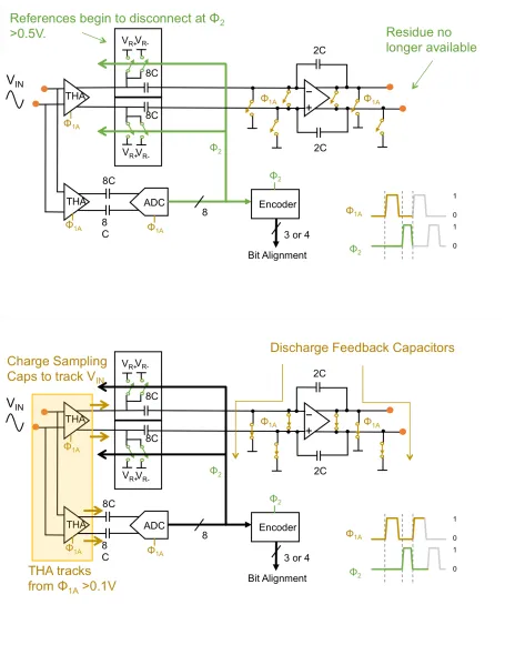
the timing diagram, the sampler, the flash stage, and the MDAC. . 27 Figure 2.7 Heirarchical top down design approach . . . 33 Figure 2.8 Non-idealities of the flash sub-ADC and the MDAC to be incorporated
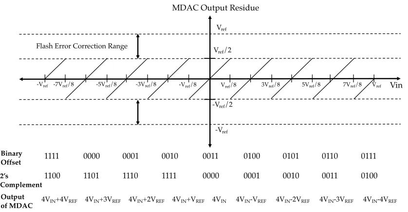
into the models. . . 34 Figure 2.9 The residue plot for a mid-tread 3-bit sub-ADC with nine subranges
[ADB+14] . . . . 34
Figure 2.10 The residue plot for a mid-rise 4-bit sub-ADC with fifteen subranges 35 Figure 2.11 Behavioral model of the opamp used in the MDAC. . . 36 Figure 2.12 An illustration of the opamp slew rate and settling behavior. . . 37 Figure 2.13 The circuit design for the pipelined ADC, here showing a single stage.
The di↵erent parts of the circuit are annotated, including (1) the sampling network (2) the 3-bit sampling flash sub-ADC (3) the logic driver for the MDAC (4) the OTA and (5) the MDAC references with the capacitor bank. . . 39 Figure 2.15 Circuit schematic showing the first design of the comparator in a
90nm BiCMOS process. . . 42 Figure 2.16 Circuit schematic showing the second design of the comparator in a
90nm BiCMOS process. . . 44 Figure 2.17 Circuit diagrams showing three kinds of possible driver logic for the
Flash sub-ADC - (a) NAND and NOT gates using CMOS logic , (b) AND gate using an Emitter Coupled Logic, and (c) NAND and NOT gates using BiCMOS logic. . . 45 Figure 2.18 Circuit schematics to illustrate the concept of BiCMOS logic. . . 46 Figure 2.19 Circuit schematic showing the modified BiCMOS design for the driver,
including the BiCMOS NAND gate, an inverter and a voltage boosting circuit. . . 47 Figure 2.20 The design of the sampling network and the bootstrapping used in
this work. . . 48 Figure 2.22 The BiCMOS design of the operational amplifier. . . 51 Figure 2.23 Small signal equivalent circuit for the first stage of the op-amp. . . 51
Figure 3.1 An illustration of the operation of a track and hold amplifier, shown here as the front-end of an ADC -multiplication of a sampled signal with a hold signal is shown as multiplication in the time domain and convolution in the frequency domain. . . 59 Figure 3.2 A zoomed image of state-of-the-art ADCs and samplers plotted in
Figure 3.3 (a)A block diagram showing a TI ADC with a sampling speed, FS,
composed of M channels, each with an ADC running at FS/M sampling
speed and (b) modified block diagram to show the dual-rank samplers used to reduce timing and bandwidth mismatches in the ADC. . . . 64 Figure 3.4 Non-linearities in a sampling waveform are compared visually and
their causes are shown conceptually. . . 66 Figure 3.5 Table delineating the cause, e↵ect and solutions of the non-linearities
caused by switching in a sampler. . . 67 Figure 3.6 Table delineating the cause, e↵ect and solutions of the non-linearities
caused by the design of the input bu↵er in a sampler. . . 67 Figure 3.7 Plot showing (i) variation of HD3 over frequency based on (3.6),
(ii) simulated HD3 of an EF in 90nm BiCMOS that compares well with (ii), and (iii) for every 100fF increase inCS,HD3 drops by 5dB, demonstrating the trade-o↵ with kT/C. . . 68 Figure 3.8 Variation of quantization noise and kT/C components of SNR where
(i) at higher resolutions, kT/C dominates SNR and (ii) decreasing it by increasing CS degrades HD3 in Fig. 3.7. . . 68 Figure 3.9 Circuit schematic of three sampler/track-and-hold amplifier
architec-tures - the switched emitter follower, the class AB Push-Pull THA, and the switched-capacitor sampler. The circuits are usually implemented fully di↵erential but are shown single-ended for simplicity. . . 70
Figure 4.1 Circuit schematic for the di↵erential design of the THA presented in this chapter. The design comprises of the input bu↵er, the track and hold stage as an SEF, and the output bu↵er. Voltages and currents used for the design are detailed. . . 76 Figure 4.2 Circuit schematic for the current-mode logic (CML) used for the clock
bu↵ers. . . 76 Figure 4.3 Chip photograph of the THA showing four stages. Also are detailed
pads for di↵erential input/output, single-ended clock input and DC biases. . . 78 Figure 4.4 Measurement setup showing the THA IC as a Device Under Test
(DUT), measured using signal generators, baluns, oscilloscope and power supply. . . 79 Figure 4.5 An iilustration of the Nyquist Zone clocking used to confirm the
operation of the circuit. . . 79 Figure 4.6 Measured di↵erential output waveform showing track-and-hold
oper-ation. A 50MHz input signal is being sampled at a 0.9GSamples/s sampling rate. . . 80 Figure 4.7 Beat Frequency test for a 40.002GHz input signal being sampled at
Figure 4.8 Measured results for P1dB from single tone measurements for 40GS/s
sampling rate. P1dB remains above 0dBm for the measured range. . 81
Figure 4.9 Measured SFDR2 and SFDR3 at 40GS/s upto 15GHz input frequen-cies. . . 81 Figure 4.10 Measured results for THD for sampling at 40GS/s. THD is calculated
at P1dB input power for large signal analysis and 10dB below P1dB for small signal analysis. . . 81 Figure 4.11 Spectrum showing intermodulation products for two tones at 14.96GHz
and 15.04GHz for 40GS/s sampling rate. . . 82 Figure 4.12 Measured results for two tone tests showing IIP3 and OIP3 for input
frequencies upto 19GHz sampled at 40GS/s. . . 82 Figure 4.13 Comparison plot showing IIP3 data of this work with existing designs
in SiGe, CMOS and InP technologies. Data is taken from cited works and is accurate within +/-0.5dB. . . 84 Figure 4.14 The state-of-the-art plot from Fig. 2.3 showing ADCs and samplers
using the Schreier FoM, annotating this work. It is shown that the 40GS/s ADC is state-of-the-art. . . 85
Figure 5.1 Block diagrams for the four test-benches simulated to analyze the performance of SHAs in BiCMOS and CMOS. (i) Case A simulates bu↵ers driving 450fF of CS. (ii) Case 2a simulates the switching distortion, (iii) Case 2b simulates tracking distortion for always-on switches for analyzing results from (ii) and (iv) Case 3 shows the complete SHA. (v) shows the (a) sample/hold switching circuitry and (b) the behavioral model of the OTA used to simulate SHAs in Cases 2a and 3. Timing diagram for switching is shown in (vi). All circuits are simulated di↵erentially and are shown single-ended for simplicity. 88 Figure 5.2 Circuit schematic for (a) an Emitter Follower in 90nm BiCMOS and
(b) a Source Follower in 28nm CMOS. . . 90 Figure 5.3 Simulation results showing (a) comparison of SFDR for bu↵er circuits
driving capacitance CS (no switches) (b) SFDR using bootstrapped switches driven by ideal bu↵ers (c) SFDR for overall SHA performance using real circuit bu↵ers and switches. . . 91 Figure 5.4 Simulation results for Case 2b, where the bu↵er is driving CS using
switches that are always-on. (a) Tracking BW versus input switch width, (b) SFDR versus input switch width. . . 92
Figure 6.1 Figure showing, for an Emitter Follower, (a) the circuit schematic and (b) the small-signal model. . . 97 Figure 6.2 Figure showing, for an Emitter Follower with the replica capacitor,
Figure 6.3 Figure showing, for a Source Follower, (a) the circuit schematic and (b) the small-signal model. . . 103 Figure 6.4 Figure showing, for a Source Follower with the replica capacitor, CR,
(a) the circuit schematic and (b) the small-signal model. . . 104 Figure 6.5 Plot showing the theoretically calculated output to input transfer
function ratio for the followers in 90nm BiCMOS, 28nm CMOS and 45nm PDSOI processes. . . 107 Figure 6.6 Plot showing the simulated output to input transfer function ratio
for the followers in 90nm BiCMOS, 28nm CMOS and 45nm PDSOI processes. . . 108 Figure 6.7 Plot comparing the theoretically calculated and simulated small-signal
current through the replica capacitor, izr. . . 108 Figure 6.8 Simulated data plotting the SFDR for three followers in 90nm
BiC-MOS, 28nm CMOS and 45nm PDSOI processes versus input frequency are shown in (a), (b) and (c) respectively. (d) shows the a comparison of the linearity performance of the three bu↵ers, at the CR values where their SFDR is optimized. . . 109 Figure 6.9 A plot of the cross section of the change in SFDR relative to the
no CR case versus CR from Fig. 6.8, showing that SFDR peaks at di↵erentCR values for the three processes. . . 110 Figure 6.10 Circuit schematic of (a) a traditional source follower and (b) a source
follower with CR. The bias devices, N3 and N4 are highlighted, and (c) plots the voltages V GS and V T H, and the source currentIS to
show the e↵ect of CR. . . 111 Figure 6.11 Circuit schematic of (a) a traditional emitter follower and (b) an
emitter follower withCR. The bias devices, Q3 and Q4 are highlighted, and (c) plots the voltage V BE and the emitter current IE to show the e↵ect of CR. . . 112 Figure 6.12 A plot of the simulated large signal current drawn by the capacitor of
460fF for an input signal of 0.5mVpp. . . 113 Figure 6.13 Simulated variation in (a) current of the emitter/source followers
Figure 6.14 Testbenches used for simulation, showing (a) a traditional emitter follower, (b) an emitter follower with an ideal current source, (c) an emitter follower linearized by using CR, composed of (d) an emitter follower with an ideal current source and CR at the base, connected to ground with (i) a full scale input voltage and (ii) half the full scale input voltage, and (e) showing (c) divided into a common-base device biased with an inductor to a dc voltage at the collector, and showing the follower device connected to incorporate any loading e↵ect. . . 115 Figure 6.15 Simulations of the three followers showing (a) the SFDR of the currents
from Fig. 6.14-d-(i) and (ii). . . 116 Figure 6.16 Circuit of a simple source follower driving a capacitive load, annotated
with bias voltage of the gate and drain, and the input and output voltage nodes. . . 117 Figure 6.17 Simulations of the three followers showing the SFDR of the currents
from Fig. 6.14-d-(ii), the source follower breakout, and Fig. 6.14-e., the common-gate breakout circuit. . . 122 Figure 6.18 Plot of HD3 and HD1 for the currents of the common-gate and source
follower amplifiers as shown in Fig. 6.14(d) and (e). . . 124 Figure 6.19 Plot showing the simulated SFDR of the SF, CG and CS currents
for Fig. 6.14-c. designed in BiCMOS, with the relative phases of the fundamental and HD3 of the CG and the SF. . . 125 Figure 6.20 Plot showing the simulated SFDR of the SF, CG and CS currents for
Fig. 6.14-c. designed in 28nm CMOS, with the relative phases of the fundamental and HD3 of the CG and the SF. . . 126 Figure 6.21 Plot showing the simulated SFDR of the SF, CG and CS currents
for Fig. 6.14-c. designed in 45nm SOI, with the relative phases of the fundamental and HD3 of the CG and the SF. . . 127 Figure 6.22 Plot showing the simulated SFDR for the three followers with
in-creasing CR, and the corresponding ratio of common-gate current to source-follower current. . . 128
Figure A.1 (a) Block diagram of a typical homodyne or low-IF receiver. The dashed line shows the receiver presented in this work. Also shown are circuit schematics of (b) the double balanced Gilbert mixer with on-chip LO/RF marchand baluns, and (c) the VGA with gain control and emitter follower bu↵ers. . . 158 Figure A.2 Illustration of step-by-step impedance transformation of the di↵
eren-tial RF impedance into a single-ended 50⌦ source. . . 161 Figure A.3 Chip photograph of the receiver detailing the single ended RF/LO
CHAPTER 1
INTRODUCTION
1.1
Motivation
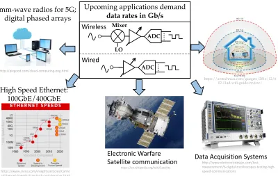
Wireless communication technologies of the near future are being enabled by frequencies at or near the millimeter-wave (mmWave) spectrum, from 30-300GHz. This is because the latter has the potential to support higher data rates that can enable ultra-broadband devices [KPR12]. There has been an exponential increase in the number of connected devices, and 5G is expected to combine very high carrier frequencies with massive bandwidths, extreme base station and device densities, and unprecedented numbers of antennas. 5G phased array antenna systems with digital beamforming rely on flexible and adaptive digital signal processing, which can be enabled by ultra-high speed ADCs. This makes ADCs instrumental for digital phased arrays, which will supply the spatial filtering required to massively increase the number of handsets supported by a single base station. Digital phased arrays would further add to the flexibility and number of simultaneous users (handsets) but further increases in ADC sample rate and bandwidth are required for digital phased arrays to emerge at 5G [ABC+14]. Over 60% of the world’s population
http://pixgood.com/cloud-computing-png.html
mm-wave radios for 5G; digital phased arrays
High Speed Ethernet: 100GbE/400GbE
https://www.ciena.com/insights/articles/Carrie r-Ethernet-Speeds-Standards-and-Services.html
Data Acquisition Systems Electronic Warfare
Satellite communication https://en.wikipedia.org/wiki/Satellite
http://www.electronicdesign.com/test- measurement/6-digital-oscilloscopes-testing-high-speed-communications
LO Mixer
ADC ....
ADC ....
https://arstechnica.com/gadgets/2016/12/8 02-11ad-wifi-guide-review/
Upcoming applications demand
data rates in Gb/s
Wired Wireless
Figure 1.1. An illustration of the wired and wireless communication applications driving the demands
for faster speeds and higher data rates for integrated solutions.
For wireline communication technologies, the current most common high speed stan-dard is 100 GbE, while 400GbE stanstan-dards are expected in the future. ON-OFF modulation techniques are becoming obsolete due to low power efficiency at high bit rates, and more sophisticated formats such as dual-polarization quadrature phaseshift keying (DP-QPSK) are being used. A DP-QPSK coherent receiver needs 4 ADC channels, since there are two optical polarizations, and each needs two ADCs to digitize an I/Q signal. To achieve 100Gb/s net line rate, a baud rate of at least 28Gbaud/s is used to allow for overhead, which needs 56Gs/s ADCs [Ded10]. Similarly, a transmitter and receiver for 100Gb/s Coherent Networks can be implemented by using four 64Gb/s ADCs [CCN+17]. The ADC
Table 1.1
Table showing ADC requirements for 100Gb/s Transmission [PHN09]
Constellation ADC BW (GHz)
ADC Sampling
Rate (GS/s) ADC ENOB
4-QAM 25 50 >3.8
16-QAM 12.5 25 >4.9
64-QAM 8.33 16.67 >5.7
256-QAM 6.25 12.5 >7
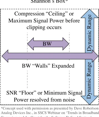
BW
BW
SNR “Floor” or Minimum Signal Power resolved from noise Compression “Ceiling” or Maximum Signal Power before
clipping occurs
D
yna
m
ic
R
ange
D
yna
m
ic
R
ange
BW “Walls” Expanded Shannon’s Box*
*Concept used with permission as presented by Dave Robertson, Analog Devices Inc., in SSCS Webinar on ‘Trends in Broadband Converters and the Quest for the Software Defined System’
Figure 1.2. Conceptual illustration of Shannon’s Box, which represents boundaries of dynamic range
and bandwidth.
1.1.1
What is the fastest data transfer that can be achieved?
Theoretically, the capacity of a channel in bits/sec is determined by the Shannon-Hartley Theorem (Eq. 1.3) as a relationship with the bandwidth (BW) of the signal and its Signal to Noise Ratio, SNR [SW63]. Wider bandwidths and higher SNR, as visualized by Shannon’s box as shown in Fig. 1.2, enable faster data rates.
SNR is a fundamental limitation to capacity, and degrades with wider bandwidths as shown in Fig. 1.3, where k is Boltzmann’s constant and T is the noise temperature. Traditionally this limitation is overcome by increasing the signal power, Psig, by increasing
the transmitted power, the antenna gain, or reduction in the receiver Noise Figure (NF). For Multiple In Multiple Out (MIMO) systems, the capacity can be even higher by a factor of M, where M is the number of antennas being used for multi-antenna transmission. However, for high speed receivers SNR may not be the fundamental limitation, which is a focus of this work.
C =BWlog2(1 +SN R) (1.1)
=BWlog2 ✓
1 + Psig
kT.BW
◆
=BWlog2
✓
1 + PtGrGt( 0
4⇡d) kT.BW.N F
◆
(1.3)
1.1.2
How faithfully can high speed data be demodulated?
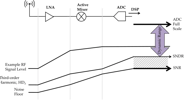
A high data rate receiver must be able to demodulate input signals faithfully. This property, also called the dynamic range, is defined within the bounds of the sensitivity of the signal from noise, and the signal compression due to non-linearity of the transfer functions receiver. Firstly, from the last section, higher data rates demand higher SNR -which a↵ects the lower end of the dynamic range. Part of the SNR referred to the input of the receiver is defined by its input referred Noise Figure (NF), which must be minimized. For high speed receivers that use Analog to Digital Converters (ADCs) for digitization of the baseband, the lower end is no longer limited by the SNR, but is instead determined by the Signal to Noise and Distortion Ratio (SNDR), as shown in Fig. 1.4. The purpose of this work is to determine how high speed receivers can be designed for higher SNDR, or lower nonlinearities, to enable a larger dynamic range.
Figure 1.3. Plot showing that data rate saturates with increasing bandwidth and SNR is a fundamental
limitation to capacity, C. However, SNR can be improved by increasing either of Pt, Antenna gain, or NF, as in Eq. 1.3.
1.1.3
What technologies enable multi-GS/s radios?
Third-order Harmonic, HD3
SNDR ADC
LNA ActiveMixer DSP
Noise Floor
ADC Full Scale
Example RF
Signal Level SNR
D
y
n
am
ic
R
an
g
e
Figure 1.4. An illustration of a typical direct-conversion radio, showing propagation of RF signal, third
order non-linearities and the noise floor. It is demonstrated that the dynamic range may be limited by the SNDR and not necessarily by the SNR.
moving to the mmWave spectrum, where for the same fractional bandwidth, much wider bandwidths are available - 10 percent fractional bandwidth at 1GHz is 100MHz, while at 100GHz it is 10GHz. Moreover, the current sub-3GHz spectrum is crowded, and mmWave transceivers can have a large number of antennas packed into a small area, due to the shorter wavelengths, thus enabling beamforming with large antenna gains [KPR12]. Advanced processes with fT and fmax in the GHz and THz range in CMOS [Sam14], SiGe
BiCMOS [SRC+16] and InP [UCG+16] have already enabled mmWave radio applications
[DPS+07] [NST+09] [LCSV09] [VGRN+11]. However, several trade-o↵s exist for the
performance in these processes, which are discussed as follows.
1.2
Choice of technology - Bulk CMOS, BiCMOS,
InP and PDSOI
1.2.1
CMOS and Bipolar processes
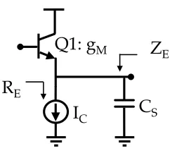
CS RE
ZE
IC
Q1: gM
Figure 1.5. The circuit schematic of the simplest analog driver, an emitter follower, showing its emitter
impedance ZEto be composed of the emitter resistance REand the sampling or load capacitance CS, the
bias current IC, and the transconductance gm.
performed. Usually the second order harmonic can be reduced or even eliminated through di↵erential circuit implementations, which makes identification and minimization of the third order harmonic an important aspect of receiver design.
A typical emitter follower bu↵er driving a capacitive load (CS), which is a fundamental
driver used in analog designs, is shown in Fig. 1.5. For this bu↵er, the gain bandwidth response is determined by the device’s transconductance, gm and sampling or parasitic
capacitance, as shown in Eq. 3.3. This reduces to a relationship between the collector current, IC, the thermal voltage VT, and CS.
GBW = gm
CS = IC
Vt . 1
CS
(1.4)
For this bu↵er, the magnitude of the third harmonic non-linearity or HD3 can be derived to be as in Eq. 3.4, where ZE is the impedance at the emitter and Vin is the
input amplitude [WS98]. ZE is defined as in Eq. 3.5 to be the impedance of the current
mirror load , and the sampling capacitance. For high frequency applications, and since the current mirror load is generally very high in output resistance RE, ZE reduces to just CS.
HD3 = 1 12.
V2 in V2 t
. 1
(gmZE)3
(1.5)
where ZE =RE|| 1
j!CS ⇡ 1
j!CS
(1.6)
Eq.3.6 represents the relationship between the third harmonic distortion of the bu↵er with its GBW, limited by CS. The HD3 in Eq. 3.6 is thus decided by Vin, which is a
HD3 =
1 12.
V2 in V2 t
. f 3 in
(GBW)3 (1.7)
The GBW is generally lower than the fT of the respective process. Since CS is typically
determined by either the load or the noise specifications of the system, the alternative to higher GBW is higher gm, in which emitter followers of Bipolar processes are superior as
compared to the source followers of CMOS processes. Thus, receivers designed with high gm HBTs benefit from a higher linearity performance.
Partially-Depleted Silicon-on-Insulator (PDSOI) processes include a thin buried oxide layer and a heavily doped substrate, which reduces the impact of several short-channel e↵ects, as the elevated substrate bias reduces short channel threshold roll-o↵. Firstly, it reduces the overall noise, with lower gate and parasitic darin/source di↵usion capacitances; secondly, it lowers the device threshold, as short channel e↵ects are lower, and thirdly, latch-up constraints are removed, since device body isolation prevents the parasitic bipolar device between FET devices. At certain bias conditions, 28nm SOI processes have been shown to strongly outperform 28nm Bulk CMOS processes in linearity. Minimization of non-linearity has been seen to appear at lower biases as compared to bulk counterparts [KEG+17].
modern HBTs enable high sensitivity in high speed receivers.
There has also been a push from specialized to mainstream technologies like CMOS by industrial partners, driven by economies of scale based on Moore’s Law. The greatest benefit for scaled CMOS for ADC design is in the digital logic, where faster switching speeds and smaller device lengths allow for better digital logic performance and reduction in the area footprint. However, highly scaled CMOS processes su↵er from lower dynamic range, intrinsic gain and output impedance, and challenging electrical, thermal and physical limitations. Scaled CMOS processes that can support RF functionality are becoming increasingly expensive from higher complexity and mask count, which makes them low cost only for large volume productions. For mmWave applications that require medium levels of volume and integration, SiGe BiCMOS processes may become more economically practical, with comparable fT/fmax and better gain and drivers for high
frequency designs than scaled RF CMOS [Sch10].
1.2.2
SiGe HBTs and InP HBTs
It should be noted that high performance HBTs are o↵ered by both InP and BiCMOS processes [SRC+16] [UCG+16]. Traditionally, InP processes have dominated power and
noise performance in the mmWave regime, but for higher cost, lower yield, and harder integration with CMOS [Cre03]. SiGe BiCMOS processes are now emerging to bridge the gap between highly scaled CMOS and high performing InP, by providing competitive integration, yield, and cost benefits [PAG+14] [Jar07]. 55nm BiCMOS is now a reality
[VCC+16] [CAR+14], with BiCMOS processes exploiting the high transconductance of
HBTs to integrate with the mixed-signal advantages of CMOS. This work thus uses an advanced SiGe BiCMOS process to enable mmWave applications.
1.3
Review of Bipolar transistors
IB B
E C
VCE VBE
VBC + -+
-+
-IE IC
E
Cut-off IC
VCE VBE0
VBE1 VBE2 VBE3 VBE4
Forward Active Saturation
BVCEO
Figure 1.6. Illustration showing the currents and voltages for a BJT device, and the IV characteristics
and regions of operation.
+
-vbe1 r!1 C!1 gm1vbe1 ro1 CE1
ib
ic
C
E B
Figure 1.7. The small signal model of the BJT is shown, with the base and collector currents and the
small-signal parameters.
from collector to emitter is denoted by ↵⇡1. The current relationship is given by
IB+IC =IE (1.8)
The variation in the output current and thus voltage is due to base width modulation, very similar to channel length modulation. As theVCE increases, the VCB becomes more reverse biased, which increases the depletion width, which increases the current IC, in turn increasing and changing VBE, thus the emitter voltage also changes. So for two di↵erent input voltages, the reverse bias will be di↵erent, and so the VBE will be di↵erent. The current relationship is exponential between the base current and the base-emitter voltage, as shown in Eq. 1.9.
IC =ISe
VBE
V T (1.9)
gm = IC VT
(1.10)
ro = VA
IC
(1.11)
Cin =gm⇤ QF
IC
(1.12)
Heterojunction Bipolar Transistors (HBTs) have a heterojunction barrier, which is implemented in the base emitter junction. This barrier reduces the parasitic injection of holes from the base in the emitter, thus giving a much higher current gain than the BJT. The base doping can be increased to decrease the base connection resistance, while still having sufficient current gain. The peak fT of a SiGe HBT improves significantly over a Si HBT, as the band o↵set at the EB junction improves the SiGe HBT frequency response [Cre98].
1.4
Focus and outline of this work
LO
Mixer IF VGA ADC TI
DSP
FS
SHA
M Channels ADC
ADC
ADC SHA
FS/M
SHA
FS/M
FS/M
SHA FS
LNA
Figure 1.8. The block diagram of a heterodyne receiver is shown, consisting of an LNA, a downconverting
mixer, and the sampling and quantization by a TI ADC sampling at FS. The dashed box on the right
shows the M-channel TI ADC, which uses dual-rank samplers, the first-rank sampler functioning at FS,
and the following M second-rank samplers operating at 1/Mth speed of F
This work focusses on the investigation of a mmWave heterodyne receiver, as shown in Fig. 1.8 to be consisting of an LNA, a mixer, and an ADC. Compared to the other two blocks, the LNA is a relatively linear component, but the mixer and the ADC, on the other hand, are strongly non-linear - the frequency translation in mixers produces numerous other frequency products with strong implications for interference and blocking, and the sampling-quantization process in ADCs introduces its own set of non-idealities. Thus, the dynamic range, speed and integration capabilities of a D-band mixer and an ADC to digitize the baseband are investigated. This work attempts to utilize BiCMOS in the traditional design philosophy of high speed, bandwidth and dynamic range radios. The research proposed here uses primarily Global Foundry’s 90nm SiGe BiCMOS process (9HP), featuring an fT=300GHz and fmax=350GHz. In addition, 9HP provides accurate
device and circuit models, high quality passive devices and metallization systems suitable for mmWave routing, and higher levels of integration and lower power consumption compared to the current 180nm or 130nm SiGe nodes [PAG+14]. The bulk of this work
focusses on ADCs, and thus the work on a D-band mixer in included in Appendix A. The digitization of the wide-band IF is proposed to be performed by a 40GS/s Time-Interleaved (TI) ADC, which uses dual-rank samplers to reduce the clock skew non-linearities. The first-rank sampler runs at the full sampling speed, 40GS/s, and the second-rank sampler can be integrated as the front-end to each channel of the TI ADC. Thus, an investigation is carried out into the design of first-rank and second-rank samplers in a 90nm BiCMOS process, and performance is compared to designs in other state-of-the-art processes such as 28nm Bulk CMOS and 45nm PDSOI. The first sampler functions at full sampling speed of 40GS/s, and is followed by dedicated samplers for each channel, which are M times slower. The design of these two samplers in BiCMOS promises not only high linearity and wide-band benefits, but also the possibility of lowering the calibration and the multi-channel interleaving requirements that are generally associated with TI ADCs. Second-rank samplers designed in 28nm CMOS and 90nm BiCMOS are compared for benefits and tradeo↵s in linearity and speed performance. It is determined that samplers designed in 90nm BiCMOS processes have performance that is comparable to samplers in 28nm CMOS. To further understand this result, the process of linearization for sampling bu↵ers using a replica capacitor technique [ADB+14] is investigated in detail,
its e↵ect on linearity in sampling bu↵ers designed in 28nm CMOS, 45nm PDSOI and 90nm BiCMOS processes is also presented.
1.5
Thesis Organization
The thesis is organized as follows. Chapter 2 presents a background on ADCs, where the e↵ects of the sampling and quantization function on the system linearity and noise are discussed. This includes a description of the various parameters used to measure the nonlinearity and noise in ADCs - SNR, SNDR, ENOB, SFDR, THD, and so on. The research in this work is then motivated through a comparison of state-of-the-art ADC architectures, particularly in the GS/s space, using the Schreier figure of merit. The 1GS/s sampling pipelined ADC architecture published in [ADB+14] is chosen for further
investigation, and its architecture, functioning and operation is illustrated by system modeling in VerilogA. Three major blocks of this ADC - the sampling network, the Flash sub-ADC comparator and driver, and the charge-redistribution OTA are chosen for circuit design in a 90nm BiCMOS process, and their performance is shown to be comparable to the published performance in 28nm CMOS, thus showing potential for high speed ADC designs in 90nm BiCMOS.
Based on the modeling and system analysis from Chapter 2, Chapter 3 chooses to focus on the sampling network block of high speed pipelined ADCs. Background is provided on the sampling and aliasing aspects of front-end samplers for ADCs, and research for this work is motivated by performing a state-of-the-art comparison, again using the Schreier figure of merit, for multi-GS/s samplers, where it is proposed that for >10GS/s first-rank samplers, fully bipolar switched emitter follower designs can be optimal, while for slower, second-rank samplers, integrated SC samplers, perhaps designed in BiCMOS processes, that can be lower power and good performance, may be ideal. The system design for samplers in TI ADCs is discussed, and background on noise and distortion of samplers is presented. Three di↵erent sampler architectures - the Switched Emitter Follower, the Class AB Push-Pull THA, and the SC Sampler - and their operation are discussed in detail.
Proceedings of the 2015 IEEE Custom Integrated Circuits Conference [LAR15]. The sampler architecture and design is presented along with its fabrication and measurement setup details, and its performance is shown to be better than previous scaled CMOS designs, and comparable to InP designs while consuming half the power of the latter.
comparing their relative nonlinearities to show how a superposition of the two provides better linearity than using the follower by itself. A methodology for design of samplers using the linearization technique from replica capacitors in di↵erent processes is presented.
Finally, in Chapter 7, this research is concluded, and future work is presented. Appendix A presents the research work for the design, fabrication, and measurement results of a state-of-the-art D-band (140-160GHz) dual side-band mixer, designed in a 90nm SiGe BiCMOS process. The text of this chapter, in part or in full, is a reprint of the material as it appears in the Proceedings of the 2016 European Microwave Conference [LAR16]. Appendix A.6 presents the results of FFT carried out on the VerilogA model of the sampling Pipelined ADC presented in Chapter 3, and Appendix C documents the VerilogA codes used in the modeling process.
1.6
Contributions of this work
Using a literature review, Chapter 2 shows that the ADC design space with sampling frequencies >5GS/s is lacking in BiCMOS designs, with predominant focus on scaled CMOS designs. One reason for this is that prior SiGe BiCMOS processes have had the CMOS node lack the Bipolar by several generations, which has made it difficult to exploit the strengths of both using true BiCMOS designs. Scaled CMOS designs also have to be extensively supported by digital calibration due to errors introduced from lower device intrinsic gains. Pipelined ADCs show a lot of potential as the key architecture for such high speeds, as they have been pushing the FoM. GlobalFoundries’ 90nm SiGe BiCMOS process has the same fT as 28nm CMOS, and both the Bipolar and the CMOS are available at 90nm. The potential of this process in enabling high performance BiCMOS ADCs still remains to be explored- prior art has designed BiCMOS ADCs using 180nm or 130nm SiGe BiCMOS. The 90nm BiCMOS process promises to have good CMOS performance, along with high HBT intrinsic gain, and together these may hold promise for design of high performance GS/s BiCMOS ADCs.
The contribution of this chapter is in the form of a detailed analysis and illustration of the functioning and operation of a 1GS/s RF sampling ADC designed in 28nm CMOS, as published in [ADB+14], through system modeling in VerilogA. This includes the operation
for bit alignment and addition. The modeling process allows for determination of the specifications of each of these blocks, for example, the gain and bandwidth requirements of the residue OTA for 1GS/s operation. The second contribution of this chapter is in demonstrating that the 90nm BiCMOS designs of the three major blocks of a pipelined ADC - the comparators for the Flash sub-ADC, the sampling network, and the OTA - are comparable in performance to the 28nm CMOS designs published in [ADB+14], and that
the design of multi-GS/s high performance pipelined ADCs in BiCMOS has substantial potential.
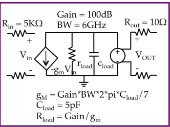
This is especially notable in the BiCMOS design of the OTA, where gain of 101dB and UGBW of 6GHz is obtained from a three-stage design. The architecture is similar to that designed for a 250MS/s Pipeline ADC in a 180nm BiCMOS process in [ADS+06].
In the design in [ADS+06], the requirements of the OTA for 16-bit performance are
100dB gain and 2GHz UGBW, but due to difficulty in obtaining that performance in the process, the requirements are relaxed and digital calibration used to fix the errors introduced. This difficulty is probably due to the lower fT of the process itself at the 180nm node, and the CMOS devices having low performance and higher parasitics due to the CMOS node lagging behind the Bipolar node, which has traditionally been the norm for BiCMOS processes. For the 1GS/s Pipeline ADC design in [ADB+14], the OTA
designed in 28nm CMOS requires a gain of 90dB and a UGBW of 6GHz, However, due to the low intrinsic gain of 28nm CMOS devices, the requirements are lowered to 75dB gain and 4GHz bandwidth, and similar to [ADS+06], significant digital calibration is
performed to subsequently reduce the errors from the residue amplification process. In this chapter, an OTA is designed in the 90nm BiCMOS process, where the fT of HBTs is 310GHz, and the CMOS is available at the same node, 90nm. The greatest advantage is from the exceptionally high gm⇤ro of the HBTs, as discussed analytically in Fig. 2.23 -where the output impedance of a single HBT is equivalent to, or even better, than that of a 3-tier MOS cascode stage. This allows for very high gain (101dB) to be obtained, without sacrificing the input and output swing requirements, and also allowing for a much higher UGBW (6GHz) than is possible from a scaled CMOS design.
digital logic, and in order to contrast it with Bipolar designs, a comparison of digital logic, Emitter-Coupled Logic, and BiCMOS logic is performed in a 90nm BiCMOS. It is shown that the power consumption and propagation delays for CMOS logic, ECL and BiCMOS logic are 0.5mW, 6mW, and 0.8mA and 100ps, 120ps and 42ps respectively. For similar propagation delays, ECL consumes an order of magnitude higher power than CMOS logic. On the other hand, BiCMOS logic consumes about 60% more power than CMOS logic, but can be much faster (at 50% lower delay) when the high speed of npn HBTs is harnessed together with 90nm CMOS switches. It should be noted that this is a first-order analysis which compares the performance of these blocks in simulation - the performance might change in post-layout simulation and with more design optimization, but as it stands, significant insight is obtained on the potential of BiCMOS ADC designs. A straightforward comparison of power consumption for these blocks could not be performed because published data was not available for the individual blocks [ADB+14, ADS+06].
This chapter sets the stage for further analysis of these blocks in di↵erent technologies. Chapter 3 chooses the front-end sampling network for multi-GS/s ADCs as critical to their overall noise and linearity performance, and through an analysis of prior state-of-the-art sampler designs, compares and contrasts the designs, architectures, and performance trade-o↵s for their implementations, particularly for Diode-based, SC and Switched Emitter Follower designs in advanced InP, CMOS and BiCMOS processes. This comparison provides preliminary information on the performance that can be achieved from sampler designs, and how linearity and sampling speeds trade-o↵ with di↵erent processes and architectures. Further, the cause, e↵ect and solutions to the various nonlinearities that arise in samplers due to the sampling bu↵ers and the sampling switches are identified and illustrated. Architectures of the Switched Emitter Follower, the Class AB Push-Pull THA, and the SC sampler are discussed, and this chapter sets the stage for high speed sampler designs in 90nm BiCMOS and other advanced processes for the following chapters.
input frequency range of 1-19GHz with a fixed clock frequency of 40GS/s. It exhibits Spurious Free Dynamic Range as high as 78dB, Total Harmonic Distortion less than -31dB and peak Input-referred 3rd order Intercept Point of 11.1dBm. The circuit has an input-referred 1dB compression point of 6dBm and consumes 560mW of power while occupying 0.03mm2 of active die area. The SFDR3 and THD3 performance is better than
similar circuits published in Silicon, and comparable to InP circuits, which consume more DC power. These results are promising for future designs of fully integrated ultra high speed transceivers in Silicon technologies.
The contribution of Chapter 5 is in presenting a methodical comparison of high-speed SC samplers in advanced processes of 28nm CMOS and 90nm BiCMOS, and demonstrat-ing, through simulated results, that their performance is comparable - specifically, the performance of a 5GS/s 90nm BiCMOS sampler is within 3-8dB of that of a 28nm CMOS sampler, both designed for the same currents and with the same architecture. It is shown that the benefits of a linearization process (using a replica capacitor) for a sampling bu↵er are much higher for a 90nm BiCMOS sampler than a 28nm sampler, while 28nm CMOS switches are faster for the sampling aspect. The research presented in this Chapter was published in the 2018 Transactions in Circuits and Systems [LAR18], as a Special Issue to the 2018 International Symposium on Circuits and Systems [dlRS18].
A final contribution is from the demonstration of a state-of-the-art 140-160GHz dual-sideband mixer, as shown in Appendix A, and published in the 2016 European Microwave Conference [LAR16]. A comparison with prior art in SiGe receivers in similar frequency ranges demonstrates this work to have the widest 3dB IF and RF bandwidths, and a compact footprint of 0.33mm2. The measured 3dB RF bandwidth extends beyond 30GHz,
while previous works have reported a maximum of 8GHz. The single sided 1dB and 3dB IF bandwidths are measured to be 10 GHz and 16 GHz respectively. This broadband performance has been achieved partly due to the co-design of the wideband Marchand baluns at the LO and RF ports, with matching networks.
1.7
Publications from this work
1.7.1
Journal Paper
D. Lal, A. M. A. Ali and D. S. Ricketts, “Analysis and Comparison of High-Resolution GS/s Samplers in Advanced BiCMOS and CMOS,” in IEEE Transactions on Circuits and Systems II: Express Briefs, vol. 65, no. 5, pp. 532-536, May 2018 (Special Issue to 2018 International Symposium of Circuits and Systems (ISCAS)).
(In Progress) D. Lal, A. M. A. Ali and D. S. Ricketts, “E↵ect of Replica Capacitor Linearization on Performance of multi-GS/s Sampling Bu↵ers,” in IEEE Transactions on Circuits and Systems - II: Express Briefs
1.7.2
Conference Papers
D. Lal, M. Abbasi and D. S. Ricketts, “A broadband, compact 140-170GHz double side-band receiver in 90nm SiGe technology,” 2016 46th European Microwave Conference (EuMC), London, 2016, pp. 687-690.
CHAPTER 2
SYSTEM AND CIRCUIT DESIGN FOR A
PIPELINED ADC
2.1
Introduction
Wideband receivers move the analog to digital interface in receivers closer to the antenna, which necessitates for the ADCs to be wideband digitizers, specifically for high speed appli-cations in instrumentation, broadband cable, military radar and wireless communication. This has many applications - electronic warfare, software defined radio, high speed radar, medical sensors and imaging, high speed reconfigurable circuits, optical communication, and direct RF sampling receiver systems. For the direct sampling purpose, since the ADC now has to sample the entire RF range, it requires a high RF acquisition bandwidth and high resolution while maintaining a small form factor and power.
2.2
Background
Po
w
e
r
SFDR
Frequency 3F1
Average Noise Floor
PIN
P3 P2
FS
2
FS P4
P5
4F1a F1 5F1a2F
1 4F1 5F1
Nyquist Region – I Nyquist Region – II
Figure 2.1. A diagrammatic illustration of the output spectrum on an ADC, often determined using a
Fast Fourier Transform (FFT). Harmonics of the fundamental frequency,F1, are shown, where a subscript
‘a’ shows harmonics that have aliased from the second Nyquist region. SFDR is shown as the di↵erence
between the fundamental and the largest spur. The average noise floor is also annotated.
ADCs provide an interface between the analog and digital domain, by performing two fundamental functions - sampling, which allows an input voltage to be converted into a discrete time value, and quantization, which approximates this voltage to a corresponding pre-determined level - and then maps the input analog signal to digital code. The combined e↵ect of these two functions is measured using a veritable ‘alphabet soup’ of performance metrics, which deal with the small signal e↵ect on noise, and the large signal limitations from spurs and distortion. The total quantization noise is given by
2 noise=
2
12 (2.1)
Non-linearities are typically visualized by looking at the harmonics of the fundamental in the frequency spectrum, as shown in Fig. 2.1. Broadly, there are two kinds of non-linearities - the first is introduced by the front-end sample-and-hold amplifier and the input amplification, and the second is due to time/amplitude quantization or encoding.
non-linearities such as Di↵erential Non-Linearity (DNL) can usually be reduced by using dither, which is a technique that sums an external noise with the analog input signal under certain conditions [Kes09a].
The theoretical Signal to Noise Ratio (SNR) of an ADC is determined by quantization noise as in Eq. 2.2, where N is the number of bits of resolution in the converter.
SN R = 6.02⇤N + 1.76 = 10⇤log10 P1
N oise (2.2)
for a sampling frequency of FS, and a Nyquist bandwidth of BW. The final term accounts for a correction factor, called process gain, that exists when the converter oversamples, i.e. when FS is much greater than twice the BW.
Quantization creates input dependent errors that result in spurs and harmonics in the output spectrum, even if the quantization function is ideal. Fig. 2.1 shows the first five harmonics of the fundamental frequency, F1. Thus another parameter, Signal to Noise and Distortion Ratio or SNDR is defined, which is a good indicator of the overall dynamic performance of an ADC.
SN DR = 10⇤log10 P1
N oise+Distortion (2.3)
SNDR is often converted to ENOB, or the E↵ective Number of Bits, as
SN DR= 6.02⇤EN OB+ 1.76 (2.4)
and indicates the total number of bits of linearity the converter could support, if SNDR were the limiting factor. It is measured over the full Nyquist region [Nyq24] (also shown as Nyquist Region - 1 in Fig. 2.1), from DC to FS/2. ENOB is necessarily calculated for a full scale input - if not, the formula changes to reflect this.
N bit converter will have all N bits appear monotonically without any of the 2N codes missing. This means that there is N-bit functioning, and the ADC indeed has N bits of resolution. The linearity from the ENOB is an indirect measure of how wide or narrow each of these codes are at the output - some are wider or narrower than the others, which means that the output may be sometimes a wrong code. This apparent resolution occurs due to non-linearities and noise, and is represented as ENOB. The bandwidth performance of an ADC system is also sometimes defined by the Error Resolution Bandwidth, or ERBW, which is the frequency at which the SNDR falls by 3dB.
The challenge to the dynamic range of the ADC is posed by spurious and harmonic sources of distortion, as indicated by SNDR, and the Spurious Free Dynamic Range (SFDR) in Fig. 2.1. SNR is not a sufficient criteria to measure the non-linearity of the ADC. This is because generally, the contribution to SNR from quantization can be reduced by increasing N, since from Eq. 2.2, every additional bit in quantization resolution improves SNR by 6dB. No such technique exists to decrease SFDR or SNDR, except perhaps that reducing the signal input by 1dB reduces the third harmonic by 2dB, but this is usually not practical since the input swing is determined by the system specifications.
The quantization of an ADC, even in a perfect case, is not fully uncorrelated to the input. Thus correlated quantization noise gathers together to make large spurs -and this is measured by using the SFDR. Moreover, the minimum detectable signal is determined both by the amount of energy present in the ADC, and also by its distribution in the frequency domain. This means that spurious quantization spurs from an unwanted frequency may fold back, or alias, either onto the desired signal band or its harmonics, and cause distortion to be dominated by a single spur [Pan99]. SFDR represents the smallest value of the signal that can be distinguished from a blocker, and the Integrated Non-Linearity (INL) of the ADC determines SFDR [Kes09c].
The system dynamic range is thus limited by the SFDR - the maximum spur - rather than the overall energy distribution by the ADC. This is because the spur may fold to any frequency in the Nyquist region - and thus it is SFDR, and not SNR, that limits the overall channel sensitivity. The SFDR should be very high so that the spurs are prevented from acting as interferers to the desired signal, and the sampling speed of the ADC should be high enough to sample and digitize wideband inputs without aliasing.