N A N O E X P R E S S
Open Access
Structural Properties Characterized by the
Film Thickness and Annealing Temperature
for La
2
O
3
Films Grown by Atomic Layer
Deposition
Xing Wang, Hongxia Liu
*, Lu Zhao, Chenxi Fei, Xingyao Feng, Shupeng Chen and Yongte Wang
Abstract
La2O3films were grown on Si substrates by atomic layer deposition technique with different thickness. Crystallization characteristics of the La2O3films were analyzed by grazing incidence X-ray diffraction after post-deposition rapid thermal annealing treatments at several annealing temperatures. It was found that the crystallization behaviors of the La2O3films are affected by the film thickness and annealing temperatures as a relationship with the diffusion of Si substrate. Compared with the amorphous La2O3films, the crystallized films were observed to be more unstable due to the hygroscopicity of La2O3. Besides, the impacts of crystallization characteristics on the bandgap and refractive index of the La2O3films were also investigated by X-ray photoelectron spectroscopy and spectroscopic ellipsometry, respectively.
Keywords:La2O3, ALD, Crystallization, Diffusion, Bandgap, Refractive index
Background
During the past decades, lanthanum oxide (La2O3) has
raised great research interests due to its remarkable chemical, thermal, optical, and electrical properties [1–3]. On the one hand, featuring with high dielectric constant (approximately 27) and large band offsets with silicon (over 2 eV), La2O3 is one among the most promising
high-k dielectric materials to replace SiO2 and Si3N4 in
advanced metal-oxide gate stack in semiconductor devices [4]. Up to now, benefiting from the approach of surface passivation prior to oxide deposition, high-quality ceria/ lanthana gate stack suitable for high-k integration in a gate-last process has been accomplished [5]. On the other hand, La2O3is usually used as a kind of effective dopant
in thermionic emitters [6], ferroelectric ceramics [7], and oxide catalysts [8], in order to improve properties such as emission capability, effective dielectric constant, and cata-lytic activity. Besides, La2O3thin films have also received
increasing attentions for the various applications in glass ceramic [9], gas sensor [10], supercapacitor [11], etc.
La2O3thin films have been prepared by various
phys-ical and chemphys-ical deposition methods, such as electron beam evaporation [12], vacuum evaporation [13], chem-ical vapor deposition [14], atomic layer deposition (ALD) [15], and molecular beam epitaxy [16]. Among the deposition methods mentioned above, due to the na-ture of the self-limited reaction, ALD has been consid-ered as one of the most promising deposition techniques to produce high quality La2O3 thin films with atomic
scale thickness controllability, fine uniformity, and excel-lent conformality [17]. La2O3thin films can be found in
several crystalline phases, namely, hexagonal (h-La2O3),
cubic (c-La2O3), amorphous (a-La2O3), or a mixture of
the phases depending on the film deposition method and post-deposition heat treatment [18]. It is well known that the structural properties of La2O3thin film are
de-termined, to a large extent, by its crystallization and microscopic morphology [19]. Therefore, the study of the crystallization and structure of La2O3thin film is of
* Correspondence:[email protected]
Key Laboratory for Wide-Band Gap Semiconductor Materials and Devices of Education, School of Microelectronics, Xidian University, Xi’an 710071, China
great significance for the compatibility of the film ap-plication into advanced electronic devices. In this art-icle, the structural properties of La2O3 thin films
prepared by ALD technique were investigated by means of a variety of measurements. Attentions were focused on the crystallization conditions of La2O3
film and the structural properties characterized by the crystalline states.
Methods
La2O3films were deposited on p-type Si (100) wafers in
an atomic layer deposition reactor (Picosun R-150) using La(i-PrCp)3 as the La precursor while O3 was used as
the oxidant. Prior to deposition of the films, native SiO2
was removed in a diluted HF solution (1:50). At the de-position temperature of 300 °C, a steady-state growth rate of ~0.85 Å/cycle is obtained by optimizing the process parameters (0.1 s La(i-PrCp)3 pulse/4 s purge
with N2/0.3 s O3 pulse/10 s purge with N2). Ten and
twenty nanometer La2O3films were prepared by varying
the number of ALD cycles. For both the 10 and 20 nm La2O3 films, post-deposition rapid thermal annealing
(RTA) was carried out at 400, 600, and 800 °C for 60 s in vacuum ambient (~1 mbar). The ellipsometric spectra of La2O3films were measured before and after annealing
by spectroscopic ellipsometry (SE) system (J.A.Woollam Co. M2000U, Lincoln, NE, USA) over the wavelength range from 245 to 1000 nm. In order to address the evolution of the crystallographic structure, grazing inci-dence X-ray diffraction (GIXRD) measurements were carried out at an angle of incidence of 1° on both the as-grown and annealed La2O3 films. Cross-sectional
high-resolution transmission electron microscopy (HRTEM) and energy-dispersive X-ray spectroscopy (EDX) line scan measurements were performed with [100] direction of the Si substrate to observe the mi-crostructures and atomic compositions of the La2O3
films. X-ray photoelectron spectroscopy (XPS) analysis
on a Theta 300 XPS system from Thermo Fisher was employed to investigate the bandgaps of the deposited films. After being exposed to air in clean room envir-onment with a relative humidity of 50% for 48 h, GIXRD and HRTEM measurements were carried out on the as-grown and annealed La2O3 films again for
further analysis.
Results and Discussion
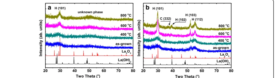
Figure 1 illustrates the GIXRD analysis performed on the as-grown and annealed La2O3 films. The powder
patterns of h-La2O3 [20] and h-La(OH)3 [21] are
added for comparison. As the GIXRD measurements were carried out immediately after the deposition and annealing process, no peaks attributed to La(OH)3
exist in the GIXRD diffractograms. The 10 nm La2O3
film (as shown in Fig. 1a) shows no diffraction fea-tures before and after a 400 °C annealing treatment, suggesting an amorphous disordered structure of the film. After being annealed at 600 and 800 °C, only weak crystalline planes such as hexagonal (101) ap-pear [22, 23], indicating the impossibility of convert-ing the 10 nm La2O3 film into complete crystalline
phase. The very small and broad peak around 50° in the diffractogram of the 10 nm La2O3 film annealed
at 800 °C does not fit to the h-La2O3 or h-La(OH)3
patterns. We think it may be formed under the influ-ence of several crystalline planes of h-La2O3 around
50°. However, for the 20 nm La2O3, the as-grown film
already shows a small degree of crystallinity with a couple of peaks attributed to h-La2O3 (as shown in
Fig. 1b). After being annealing treated, the intensities of the GIXRD peaks increase, which means the en-hancement in the degree of crystallinity. After anneal-ing at 600 °C, except for the weak cubic (332) plane [14], the film was mainly crystallized to hexagonal phase as the GIXRD diffractograms exhibit strong hexagonal planes such as (101), (102), (103), and
a
b
Fig. 1GIXRD diffractograms of as-grown and annealed La2O3films deposited on Si substrate.a10 andb20 nm La2O3films. Hexagonal La2O3
[image:2.595.59.541.565.702.2](112). Besides, further increase in the annealing temperature up to 800 °C does not seem to signifi-cantly affect the GIXRD diffractograms of the film. That is, upon 600 °C, the increase in the annealing temperature does not enhance the crystallinity of the film. Consequently, when annealed upon 600 °C, an almost complete crystallization could be accomplished for the 20 nm La2O3film.
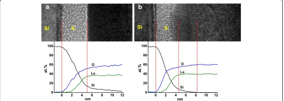
Additional structural information at the La2O3/Si
interface after RTA treatment at 600 °C is provided by HRTEM-EDX analysis as shown in Fig. 2. For both 10 nm (Fig. 2a) and 20 nm (Fig. 2b) La2O3films, the
lan-thanum and oxygen in-depth distributions in the EDX elemental ratio profiles show a parallel profile and the La/O ratio is close to 2:3 which meets well with the stoi-chiometry of La2O3. In the HRTEM images, an
amorph-ous region between the Si substrate and the fabricated film, corresponding to an interfacial layer (IL) formed during the ALD growth and RTA process [24], could be found in both Fig. 2a, b. After the amorphous IL, it is possible to identify a region containing nanometer-sized crystals in the 10 nm La2O3 film, indicating the
exist-ence of an incomplete structural conversion (from amorphous to crystallographic structure) during the RTA treatment. However, the structure of the 20 nm La2O3film is a little complicated. With the guidance of
dotted lines, an amorphous region, a nanometer-sized crystal transition region, and a long-range ordered crys-tal region could be observed in the HRTEM image of Fig. 2b. The presence of long-range ordered crystals manifests, in accordance with the GIXRD results shown in Fig. 1, that RTA process upon 600 °C induces an al-most complete crystallization of the 20 nm La2O3film.
It is worth noting that upon the same annealing condi-tion of at 600 °C for 60 s in vacuum ambient (~1 mbar), the 10 and 20 nm La2O3films show different crystalline
characteristics. We attribute this difference to the RTA-induced Si diffusion from the substrate into the La2O3
layer [25]. As we know, La2O3exhibits the highest
affin-ity for Si atoms among the rare-earth oxide films due to the so called “lanthanide contraction” property of rare-earth elements [26]. Even in the as-deposited La2O3film
grown by ALD method, substrate silicon atoms diffuse moderately and distribute in gradient from Si substrate to the upper layer, causing the presence of an IL about 1 nm [27, 28]. Besides, part of the as-deposited La2O3
film close to the IL could be considered as Si-riched and difficult to crystallize as Si rich help to prevent the for-mation of crystalline La2O3 precipitates [29].
Further-more, post-deposition annealing causes extra silicon out diffusion and reaction with excess oxygen in the film. Consequently, in thin La2O3 film with the thickness of
10 nm or less, during the annealing process, the sub-strate Si atoms would diffuse deep easily to the upper layer before the film is crystallized. However, for the 20 nm as-deposited La2O3, since Si atoms distribute in
gradient from Si substrate to the upper layer, a great part of the film relatively far away from Si substrate is pure. We think that this part of La2O3 film could be
crystal-lized at appropriate post-deposition treatment such as RTA carried out at 600 and 800 °C for 60 s in vacuum ambient (~1 mbar) in this work. Crystallization of the film brings in an aggressive enhancement in the packing density and thermodynamic stability. Thus, to a certain extent, the diffusion of Si atoms from substrate into the upper layer would be restrained. As a result, the silicate layer of the 20 nm La2O3 film is slightly thinner than
what could be observed in the 10 nm La2O3 film.
Be-sides, in the 20 nm La2O3 film, only 3~4 nm La2O3
closed to the IL was converted into nanometer-sized crystals under the influence of Si diffusion during the annealing process. Complete crystallization of the
[image:3.595.57.541.541.714.2]grown film into the h-La2O3 phase is achieved in the
region not affected by Si diffusion.
The bandgaps of the as-grown and annealed (at 600 °C) La2O3 films were measured by examining the
energy loss of the O 1s core levels as shown in Fig. 3. As we know, the bandgap equals the energy distance between the photoemission peak centroid and the on-set of the features due to single particle excitations, and it is usually obtained from the inelastic energy loss features observed on the high binding energy side of the core level photoemission peaks [30]. The onset of O 1s loss spectrum was determined by linearly ex-trapolating the segment of maximum negative slope to the back ground level [31]. The bandgaps of the as-grown 10 and 20 nm La2O3 films are determined
to be 5.55 and 5.45 eV, respectively. These values are in fairly good agreement with Ohmi et al. [32], who have reported a bandgap of 5.50 eV for non-crystallized La2O3 on Si substrate. The bandgap of
the annealed 20 nm La2O3 film is determined to be
5.20 eV, which agrees well with the bandgap of 5.30 eV for crystallized La2O3 reported by Zhao et al.
[33]. However, the diffusion of Si during the anneal-ing process branneal-ings in large mounts of La-O-Si bonds for the 10 nm La2O3, leading to the increase of the
inelastic energy loss during the transition from valence band to conduction band, which means the
increment of bandgap [34]. As a result, the bandgap of the annealed 10 nm La2O3is figured out as 6.0 eV,
which is evidently larger than the bandgap of crystal-lized La2O3.
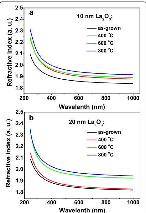
Figure 4 illustrates the annealing temperature depend-ence of refractive indexes for the as-grown and annealed La2O3films revealed by SE fitting. The refractive indexes
of the La2O3films were determined by fitting the
ellip-sometry data using the well-known Tauc-Lorentz disper-sion mode, which was proposed by Jellison and Modine and has been successfully applied to a variety of amorph-ous and crystallized materials [35–37]. As revealed in Fig. 4, the refractive indexes of the as-grown La2O3films
increase with varying degrees after being annealed at dif-ferent temperatures. It was reported that the refractive index is closely related to the density of materials, being lower at lower density. Consequently, the increase in the refractive index is caused by the stress release and densi-fication during the annealing process [38, 39]. Further-more, for the 20 nm La2O3 film, an abrupt increase in
the refractive index could be observed when the anneal-ing temperature increased from 400 to 600 °C, indicatanneal-ing an aggressive enhancement in the packing density upon crystallization. As a result, after being annealed at 600 °C, the 20 nm La2O3 film shows an index of refraction of
1.943 at the wavelength of 632.8 nm, which is much higher than that of the as-grown film (1.838). The
Fig. 3Bandgaps for the La2O3films with different thickness and annealing temperatures.aas-grown 10 andb10 nm La2O3annealed at 600 °C,
[image:4.595.59.539.442.703.2]refractive indexes obtained in this work are of good com-parability with the results reported by Armelao et al. [1] and Kukli et al. [40].
Figure 5 illustrates the GIXRD diffractograms for the as-grown and annealed La2O3films after being exposed
to air in clean room environment with a relative humid-ity of 50% for 48 h. Compared with the GIXRD diffrac-tograms obtained before the air exposure as displayed in Fig. 1, almost all the GIXRD peaks attributed to h -La2O3 disappear, whereas new peaks attributed to h
-La(OH)3appear due to the hygroscopicity of La2O3[22,
23, 41]. It is noteworthy that strong h-La(OH)3phase
peaks are only found in the well crystallized samples such as the 20 nm La2O3 films annealed at 600 and
800 °C, while few weak peaks are observed in the amorphous disordered and nanometer-sized crystallo-graphic samples. Besides, it seems that the air exposure has a much heavier effect on the 20 nm La2O3 than
that on the 10 nm La2O3. For clarity, cross-sectional
HRTEM measurements on the annealed 10 and 20 nm La2O3films after the air exposure were performed. The
cross-sectional HRTEM image of the annealed 20 nm La2O3after being exposed to air is shown in Fig. 6b, in
which much more uneven interface and surface are ob-served than what can be found in the 10 nm La2O3.
The deteriorations in the interface and surface proper-ties are attributed to the degradation in the film density caused by the conversion from h-La2O3 to h-La(OH)3.
With the time exposed to air, the amount of La(OH)3
in La2O3film increases and then the density of the film
is degraded, resulting in the changes of the surface and interfacial morphologies [42]. However, the existence of large mounts of LaSiO in the 10 nm La2O3 enhances
the stability of the film structure, providing a high im-munity against moisture ambient.
Conclusions
The crystallization of La2O3 film grown by atomic
layer deposition on Si substrate is restricted by the thickness of the film and the post-deposition annealing temperature. For thin (~10 nm) La2O3 film, only
nanometer-sized crystals are formed after the anneal-ing treatment due to the diffusion of Si substrate. For
Fig. 4Annealing temperature dependence of refractive index for ALD-La2O3with different thickness.a10 nm La2O3films andb20
nm La2O3films
Fig. 5GIXRD diffractograms for as-grown and annealed La2O3after being exposed to air for 48 h.a10 nm La2O3films annealed at 600 °C and
[image:5.595.57.290.86.427.2] [image:5.595.56.542.563.703.2]thick (~20 nm) La2O3, films can be mainly crystallized
intoh-La2O3upon RTA performed in vacuum
environ-ment at 600 °C. After being crystallized, the refractive index of La2O3 film increases dramatically, while the
bandgap is slightly decreased. After an exposure to air for 48 h, the h-La2O3 films are converted into h
-La(OH)3due to the hygroscopicity of La2O3.
Abbreviations
ALD:Atomic layer deposition; EDX: Energy dispersive X-ray spectroscopy; GIXRD: Grazing incidence X-ray diffraction; HRTEM: High-resolution transmission electron microscopy; IL: Interfacial layer; RTA: Rapid thermal annealing; SE: Spectroscopic ellipsometry; XPS: X-ray photoelectron spectroscopy
Funding
The authors gratefully acknowledge the financial supports for this work from the National Natural Science Foundation of China (grant nos. 61376099 and 61434007) and the Foundation for Fundamental Research of China (grant no. JSZL2016110B003). The National Natural Science Foundation of China and the Foundation for Fundamental Research of China did neither participate in the design of the study nor in the collection, analysis, and interpretation of data or the writing of the manuscript. We are very grateful to Dr. Yanlin Pan for the valuable assistance and excellent technical support for the HRTEM-EDX measurements.
Authors’Contributions
XW generated the research idea, analyzed the data, and wrote the paper. XW and LZ carried out the experiments and measurements. XyF and CxF participated in the discussions. SpC and YtW gave kind suggestions about the experiments and measurements. HxL has given final approval of the version to be published. All authors read and approved the final manuscript.
Authors’Information
XW, LZ, and CxF are PhD students in Xidian University. HxL is a professor in Xidian University. XyF and YtW are Master students in Xidian University.
Competing Interests
The authors declare that they have no competing interests.
Publisher’s Note
Springer Nature remains neutral with regard to jurisdictional claims in published maps and institutional affiliations.
Received: 3 December 2016 Accepted: 20 March 2017
References
1. Armelao L, Pascolini M, Bottaro G, Bruno G, Giangregorio MM, Losurdo M, Malandrino G, Lo Nigro R, Fragalà ME, Tondello E (2009) Microstructural and optical properties modifications induced by plasma and annealing treatments of lanthanum oxide sol–gel thin films. J Phys Chem C 113:2911–2918 2. Wei C, Fan JL, Gong HR (2015) Structural, thermodynamic, and mechanical
properties of bulk La and A-La2O3. J Alloy Compd 618:615–622
3. Richard D, Errico LA, Rentería M (2015) Electronic, structural, and hyperfine properties of pure and Cd-doped hexagonal La2O3semiconductor. Comp
Mater Sci 102:119–125
4. Kim WH, Maeng WJ, Moon KJ, Myoung JM, Kim H (2010) Growth
characteristics and electrical properties of La2O3gate oxides grown by thermal
and plasma-enhanced atomic layer deposition. Thin Solid Films 519:362–366 5. Flege JI, Kaemena B, Schmidt T, Falta J (2014) Epitaxial, well-ordered ceria/ lanthana high-k gate dielectrics on silicon. J Vac Sci Technol B 32(3):03D124 6. Hoebing T, Hermanns P, Bergner A, Ruhrmann C, Traxler H, Wesemann I,
Knabl W, Mentel J, Awakowicz P (2015) Investigation of the flickering of La2O3and ThO2doped tungsten cathodes. J Appl Phys 118:023306
7. Wei LL, Yang ZP, Chao XL, Jiao H (2014) Structure and electrical properties of Ca0.28Ba0.72Nb2O6ceramics with addition of rare earth oxides (CeO2,
La2O3). Ceram Int 40:5447–5453
8. Wang N, Liu JJ, Gu WW, Song Y, Wang F (2016) Toward synergy of carbon and La2O3in their hybrid as an efficient catalyst for the oxygen reduction
reaction. RSC Adv 6:77786–77795
9. Yoshimoto K, Masuno A, Inoue H, Watanabe Y (2012) Transparent and high refractive index La2O3–WO3glass prepared using containerless processing.
J Am Ceram Soc 95(11):3501–3504
10. Ehsani M, Hamidon MN, Toudeshki A, Shahrokh Abadi MH, Rezaeian S (2016) CO2gas sensing properties of screen-printed La2O3/SnO2thick film.
IEEE Sens J 16(18):6839–6845
11. Yadav AA, Kumbhar VS, Patil SJ, Chodankar NR, Lokhande CD (2016) Supercapacitive properties of chemically deposited La2O3thin film.
Ceram Int 42:2079–2084
12. Wong H, Yang BL, Kakushima K, Ahmet P, Iwai H (2012) Effects of aluminum doping on lanthanum oxide gate dielectric films. Vacuum 86:929–932 13. Dakhel AA (2007) Structural and ac electrical properties of oxidized La and
La–Mn thin films grown on Si substrates. Mater Chem Phys 102:266–270 14. Kim HJ, Jun JH, Choi DJ (2008) Characteristics of La2O3thin films deposited
using metal organic chemical vapor deposition with different oxidant gas. Ceram Int 34:953–956
15. Wiemer C, Lamagna L, Fanciulli M (2012) Atomic layer deposition of rare-earth-based binary and ternary oxides for microelectronic applications. Semicond Sci Technol 27:074013
16. Kakushima K, Tachi K, Ahmet P, Tsutsui K, Sugii N, Hattori T, Iwai H (2010) Advantage of further scaling in gate dielectrics below 0.5 nm of equivalent oxide thickness with La2O3gate dielectrics. Microelectron Reliab 50:790–793
17. Yang W, Sun QQ, Fang RC, Chen L, Zhou P, Ding SJ, Zhang DW (2012) The thermal stability of atomic layer deposited HfLaOx: material and electrical
characterization. Curr Appl Phys 12:1445–1447
a
b
Fig. 6HRTEM images for the annealed La2O3films after being exposed
to air for 48 h.a10 nm La2O3film annealed at 600 °C andb20 nm
[image:6.595.56.290.86.440.2]18. Ramana CV, Vemuri RS, Kaichev VV, Kochubey VA, Saraev AA, Atuchin VV (2011) X-ray photoelectron spectroscopy depth profiling of La2O3/Si thin films deposited
by reactive magnetron sputtering. ACS Appl Mater Inter 3:4370–4373 19. Song JB, Lu CH, Xu D, Ni YR, Liu YJ, Xua ZZ, Liu JX (2010) The effect of
lanthanum oxide (La2O3) on the structure and crystallization of poly
(vinylidene fluoride). Polym Int 59:954–960
20. Inorganic Crystal Structure Database (2009) Fachinformationszentrum, Karlsruhe., file No. 24693
21. Inorganic Crystal Structure Database (2009) Fachinformationszentrum, Karlsruhe., file No. 31584
22. Hu CG, Liu H, Dong WT, Zhang YY, Bao G, Lao CS, Wang ZL (2007) La(OH)3and
La2O3nanobelts—synthesis and physical properties. Adv Mater 19:470–474
23. Aghazadeh M, Arhami B, MalekBarmi AA, Hosseinifard M, Gharailou D, Fathollahi F (2014) La(OH)3and La2O3nanospindles prepared by
template-free direct electrodeposition followed by heat-treatment. Mater Lett 115:68–71 24. Lee WJ, Ma JW, Bae JM, Kim CY, Jeong KS, Cho MH, Chung KB, Kim H, Cho HJ, Kim DC (2013) The diffusion of silicon atoms in stack structures of La2O3and
Al2O3. Curr Appl Phys 13:633–639
25. Park TJ, Sivasubramani P, Wallace RM, Kim J (2014) Effects of growth temperature and oxidant feeding time on residual C- and N-related impurities and Si diffusion behavior in atomic-layer-deposited La2O3thin
films. Appl Surf Sci 292:880–885
26. Ono H, Katsumata T (2001) Interfacial reactions between thin rare-earth-metal oxide films and Si substrates. Appl Phys Lett 78:13
27. Lamagna L, Wiemer C, Perego M, Volkos SN, Baldovino S, Tsoutsou D, Schamm-Chardon S, Coulon PE, Fanciulli M (2010) O3-based atomic layer
deposition of hexagonal La2O3films on Si (100) and Ge (100) substrates.
J Appl Phys 108:084108
28. Kim H, Woo S, Lee J, Kim H, Kim Y, Lee H, Jeon H (2010) The effects of annealing ambient on the characteristics of La2O3films deposited by
RPALD. J Electrochem Soc 157:H479–H482
29. Wilka GD, Wallace RM (1999) Electrical properties of hafnium silicate gate dielectrics deposited directly on silicon. Appl Phys Lett 74:2854–2856 30. Bell FG, Ley L (1988) Photoemission study of SiOx(0≤x≤2) alloys. Phys Rev B
37:8383–8393
31. Liu QY, Fang ZB, Liu SY, Tan YS, Chen JJ (2014) Band offsets of La2O3films
on Ge substrates grown by radio frequency magnetron sputtering. Mater Lett 116:43–45
32. Ohmi S, Kobayashi C, Kashiwagi I et al (2002) Characterization of La2O3and
Yb2O3thin films for high-k gate insulator application. Electrochem Soc
150(7):F134–F140
33. Zhao Y, Kita K, Kyuno K, Toriumi A (2009) Band gap enhancement and electrical properties of La2O3films doped with Y2O3as high-k gate insulator.
Appl Phys Lett 94:042901
34. Zhang F, Saito K, Tanaka T, Nishio M, Arita M, Guo Q (2014) Wide bandgap engineering of (AlGa)2O3films. Appl Phys Lett 105:162107
35. Jellison GE Jr, Modine FA (1996) Parameterization of the optical functions of amorphous materials in the interband region. Appl Phys Lett 69:371–373 36. He G, Zhu LQ, Liu M, Fang Q, Zhang LD (2007) Optical and electrical
properties of plasma-oxidation derived HfO2gate dielectric films. Appl
Surf Sci 253:3413–3418
37. Giannakopoulou T, Todorova N, Giannouri M, Yu J, Trapalis C (2014) Optical and photocatalytic properties of composite TiO2/ZnO thin films. Catal Today
230:174–180
38. Wang ZY, Zhang RJ, Lu HL, Chen X, Sun Y, Zhang Y, Wei YF, Xu JP, Wang SY, Zheng YX, Chen LY (2015) The impact of thickness and thermal annealing on refractive index for aluminum oxide thin films deposited by atomic layer deposition. Nanoscale Res Lett 10:46
39. Nayar P, Khanna A, Kabiraj D, Abhilash SR, Beake BD, Losset Y, Chen BH (2014) Structural, optical and mechanical properties of amorphous and crystalline alumina thin films. Thin Solid Films 568:19–24
40. Kukli K, Ritala M, Pore V, Leskelä M, Sajavaara T, Hegde RI, Gilmer DC, Tobin PJ, Jones AC, Aspinall HC (2006) Atomic layer deposition and properties of lanthanum oxide and lanthanum-aluminum oxide films. Chem Vap Deposition 12:158–164
41. Calmels L, Coulon PE, Schamm-Chardon S (2011) Calculated and experimental electron energy-loss spectra of La2O3, La(OH)3, and LaOF nanophases in high
permittivity lanthanum-based oxide layers. Appl Phys Lett 98:243116 42. Zhao Y, Toyama M, Kita K, Kyuno K, Toriumi A (2006)
Moisture-absorption-induced permittivity deterioration and surface roughness enhancement of lanthanum oxide films on silicon. Appl Phys Lett 88:072904
Submit your manuscript to a
journal and benefi t from:
7Convenient online submission
7Rigorous peer review
7Immediate publication on acceptance
7Open access: articles freely available online
7High visibility within the fi eld
7Retaining the copyright to your article