N A N O E X P R E S S
Open Access
Indium-doped ZnO nanowires with infrequent
growth orientation, rough surfaces and
low-density surface traps
Hongfeng Duan, Haiping He
*, Luwei Sun, Shiyan Song and Zhizhen Ye
*Abstract
Indium-doped ZnO nanowires have been prepared by vapor transport deposition. With increasing In content, the growth orientation of the nanowires switches from [1010] to infrequent [0223] and the surface becomes rough. No surface-related exciton emission is observed in these nanowires. The results indicate that large surface-to-volume ratio, high free electron concentration, and low density of surface traps can be achieved simultaneously in ZnO nanowires via In doping. These unique properties make In-doped ZnO nanowire a potential material for
photocatalysis application, which is demonstrated by the enhanced photocatalytic degradation of Rhodamine B.
Keywords:In-doped ZnO nanowires; Infrequent [0223] growth orientation; Large surface-to-volume ratio; Low density of surface traps
Background
One-dimensional (1D) ZnO nanostructures have attrac-ted extensive research interests in the past decade due to their versatile application potential in nanooptoelec-tronics [1], electromechanics [2], and catalysis [3]. It has been found that doping impurities, especially group III elements, such as Al [4], Ga [5], In [6], can significantly enhance the electrical conductivity and influence the op-tical properties. In order to generate desirable electrical, optical, and catalytic properties, 1D ZnO nanostructures have been doped with selected elements. Among these dopants, In is recognized as one of the most efficient elements used to tailor the optoelectronic properties of ZnO [7]. For example, In doping may induce structural defects such as stacking faults [8], twin boundaries [9], and superlattice structures [10], or result in weak lo-calization and electron–electron interactions [11], which can significantly affect the electrical and photolumines-cence (PL) properties of ZnO nanostructures. On the other hand, it is quite interesting that In doping can change the morphology of ZnO nanowires (NWs) [12]. There are three typical fast-growth directions ([0001],
[1010], and [112 0]) and ± (0001) polar surfaces in wurtzite ZnO [13]. In general, ZnO NWs grow along [0001] di-rection. When doped with In, however, they may grow along some other directions, such as the non-polar [0110] direction [14].
ZnO nanostructures usually have plenty of surface states acting as carrier traps. The existence of such traps is unwanted in catalytic applications, which take advan-tage of free carriers in the surface region of ZnO nano-structures. In this regard, ZnO nanostructures with large surface-to-volume ratio, high free electron concentra-tion, and low density of surface traps are highly desired.
In this work, we demonstrated that such ZnO nano-structures can be achieved via In doping. The In-doped ZnO NWs were grown by one-step vapor transport de-position. The effect of In doping content on the morph-ology, structure, and optical properties of the NWs has been investigated. With increasing In doping content, ZnO NWs show switches of the orientation from [1010] to an infrequent [0223] direction and surface from smooth to ripple-like. Low-temperature PL spectra in-dicate that indium indeed acts as shallow donor and the density of surface traps is very low. We demons-trated the enhanced photocatalytic performance of In-doped ZnO NWs by degradation of Rhodamine B (RhB) solution.
* Correspondence:[email protected];[email protected]
Department of Materials Science and Engineering, State Key Laboratory of Silicon Materials, Cyrus Tang Center for Sensor Materials and Applications, Zhejiang University, Hangzhou 310027, People's Republic of China
Methods
The In-doped ZnO nanowires were synthesized by a vapor transport deposition process in a single-zone high-temperature tube furnace. A mixture of ZnO (99.999%), graphite (99.9%), and In2O3(99.99%) powder (weigh ratio
8:2:1) was used as the source material. A layer of 5-nm gold film deposited on the Si (100) substrate before the growth of ZnO NWs was used as catalyst. Then the treated silicon substrate and the source material were placed in a quartz boat and inserted into the tube furnace. Si (100) substrate was placed about 10 cm downstream of the source. Before growth, the quartz tube was evacuated to about 100 mTorr by a rotary pump. Then the tube fur-nace was heated to 950°C at a rate of 20°C min−1, under a Ar flow rate of 100 standard-state cubic centimeter per minute (SCCM). When the temperature reached 950°C, high purity O2 was continuously fed into the tube at a
flow rate of 2 SCCM, and the pressure was maintained at 4 Torr. After reacting for 30 min at 950°C, the furnace was naturally cooled to room temperature without O2
flux, and the white product deposited on the silicon sub-strate was collected. Undoped ZnO NWs were also grown under the same experimental conditions.
The structure and composition of the samples were analyzed by X-ray diffraction (XRD) through a Rigaku D/max 2550 pc diffractometer (The Woodlands, Texas, USA) and secondary ion mass spectroscopy (SIMS) on a time-of flight mass spectrometer (Ion TOF-SIMS). The morphology and microstructure of the nanowires were characterized by scanning electron microscopy (SEM, Hitachi S-4800, Tokyo, Japan) and transmission electron microscopy (TEM, Philips-FEI Tecnai G2 F30 S-Twin, Hillsboro, OR, USA) combined with selective area elec-tron diffraction (SAED). The In doping content of the individual NW was confirmed by energy disper-sive X-ray spectroscopy (EDX) equipped in the TEM instrument. PL spectra were measured on a fluores-cence spectrometer (FLS920 Edinburgh Instruments, Livingston, West Lothian, UK), using a He-Cd 325-nm laser as the excitation source.
The photocatalytic activity of the nanowires was evalu-ated by investigating the photocatalytic degradation of RhB in aqueous solution in a cylindrical quartz photo-reactor. Thirty milligrams of each sample was dispersed in 100 ml of deionized water, followed by ultrasonication for 1 h. One milliliter of 1 mM RhB aqueous solution was then added. A Xe lamp was used as the illumination source. Before illumination, the solution was stirred con-tinuously in the dark for 30 min to reach an adsorption-desorption equilibrium of dye molecules on the surface of photocatalysts. The concentration of the remaining dyes was monitored by measuring the absorbance of the solution using a UV–vis spectrophotometer (Shimadzu 3600, Tokyo, Japan).
Results and discussion
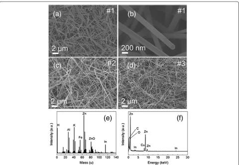
Figure 1a,b shows the low- and high-magnification top-view SEM images of the undoped ZnO nanorods (labeled #1). The sample consists of straight nanorods with uniform diameter of about 200 nm. The uniform hexagonal nanorods are preferentially grown along [0001] direction with smooth surface. Figure 1c,d shows the morphology of the ZnO NWs doped with different In content. It can be seen clearly that the morphology and diameter have changed after In doping. These two sam-ples have similar density and diameter, but the concentra-tion of In dopant are quite different. The In content of the sample showed in Figure 1c (labeled #2) is too low to be detected by EDX, but can be measured by SIMS, as shown in Figure 1e. The ZnO NWs shown in Figure 1d (labeled #3) is heavily doped with In, and the average amount of In in individual NW is about 1.4 at.%, as demonstrated by EDX in Figure 1f.
X-ray diffraction was carried out to investigate the structure of the three samples. As shown in Figure 2, the patterns reveal that all the samples have hexagonal wurtzite ZnO structure and no extra peak is observed, except the Au (111) and Au (200) peaks, indicating that no secondary phase exists in all of the three samples. The results suggest the successful incorporation of In into ZnO lattice without altering the crystal structure.
in the embossment part are 0.283 and 0.248 nm which match those of the (1010) and (1011) planes, respectively. This result indicates that the (0 1 11) is the dominant plane, and the NWs mainly grow along an infrequent direction of [02 2 3]. As the growth approaches the ripple-like edge, the (10 10) and (10 11) facets emerge, and the edge of surface becomes zigzag. Such crystal planes and orientation are not common for ZnO. It is noteworthy that the growth along [0001] direction is suppressed in both of the two In-doped samples. These results definitely indicate that incorporation of In ions into ZnO NWs can promote the tendency of orientation change from the c-axis [0001] to an infrequent [02 23] direction. We believe that the change of preferred orien-tation is due to the change of surface energy of ZnO planes upon In doping, and the energy difference and relative stability among the (0001), (10 10), and (0 111) surfaces vary with increasing doping concentration. Un-fortunately, theoretical calculations of the surface energy change are unavailable at this moment. However, it is Figure 2XRD patterns of ZnO NWs.Full pattern of undoped (#1)
[image:3.595.57.291.513.695.2]and In-doped (#2, #3) ZnO NWs. No secondary phase is observed in all of the three samples.
Figure 1SEM images and SIMS and EDX spectra. (a)Low and(b)high magnification SEM images of the undoped ZnO nanorods (#1).
noteworthy that analogous orientation changes have been observed in Mn-doped ZnO films and testified by the calculation results [15].
PL is an excellent method to investigate the impurity and surface states in semiconductors. The optical signa-ture of donor impurities in ZnO has been well estab-lished by examining the donor-bound exciton (DBE) emission. On the other hand, due to the large surface-to-volume ratio of ZnO nanostructures, the emission from surface excitons (SX), generally appears around 3.366 eV, has been frequently observed in low tem-perature PL spectra of many ZnO nanostructures with various morphologies [16-18]. The low-temperature PL (LT-PL) spectra of the three samples at 14 K are plotted in Figure 4a. In the undoped ZnO NWs (#1), the DBE peak locates at 3.360 eV, which corresponds to residual donors, such as Al (I6) [19]. In the PL spectra of
In-doped ZnO NWs (#2 and #3); however, the DBE peak shifts to 3.357 eV, which is known as I9 line and is
unambiguously attributed to the exciton bound to In
donors [19,20]. This confirms that In is in the substitu-tion site and acts as shallow donor. The emission around 3.31 eV has been a controversial issue for a long time [21-23]. From the low-temperature PL spectra, one can find that the peak around 3.31 eV is observed in both of the two In-doped samples, but not for the undoped one. Furthermore, a direct correlation is found between the intensity of the 3.31 eV emission and the In-doping concentration. Recently, Schirra et al. [21] presented convincing evidences that the 3.31 eV emission in ZnO is related to stacking faults. In our work, the increase of the 3.31 eV emission with In content is consistent with the phenomenon that In doping can easily induce stack-ing faults in ZnO nanostructures [8]. Therefore, we sug-gest that the 3.31 eV emission most probably originates from the stacking faults induced by In doping.
[image:4.595.55.292.88.422.2]From the TEM images (Figure 3c,d), we can observe that the high-content In-doped ZnO NWs have ripple-like surface, which can result in a much larger surface-to-volume ratio and thus facilitate the formation of SXs. Figure 3TEM images and corresponding SAED patterns of
In-doped ZnO NWs. (a)TEM image,(b)HRTEM image and its corresponding SAED pattern (inset) of sample #2.(c,d)TEM images,
[image:4.595.309.540.89.432.2](e,f)HRTEM images and its corresponding SAED pattern (inset) of sample #3.
Figure 4PL spectra of ZnO NWs. (a)Low-temperature (14 K) and
Therefore, remarkable surface state-related emission would have been expected in our sample. However, no SX-related emission peak (approximately 3.366 eV) is ob-served in the low-temperature PL spectrum of sample #3, as shown in Figure 4a. Moreover, the deep level emission, which is found to largely originate from surface defects
[24], decreases with increasing In-doping concentration (Figure 4b). These results indicate that the influence of the surface states on the PL properties of sample #3 is almost negligible, which strongly suggests that the density of surface electron traps is at a very low level in our sample.
The realization of ZnO nanostructures with large surface-to-volume ratio and low density of surface traps may enhance the photocatalytic performance. To evalu-ate the photocatalytic activities of In-doped ZnO NWs, degradation of RhB in aqueous solution was investigated. Figure 5 shows the results of RhB photo-degradation over undoped and In-doped ZnO NWs. It was evident that the ZnO NWs with high In doping content (#3) ex-hibited much better photocatalytic performance than the undoped one. After illuminating for 100 min, sample #3 was found to degrade nearly 73% of the initial RhB dye, while the degradation over undoped ZnO NWs was less effective, only 20% within the same irradiation time. It is well known that the photocatalytic activities of semicon-ductor materials are closely related to their morphology, structure and surface properties [25]. Therefore, the much improved photocatalytic performance of In-doped ZnO NWs is probably associated with their large surface-to-volume ratio and low density of surface traps.
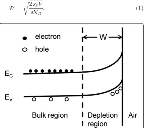
Moreover, high concentration of shallow In donors results in high concentration of free electrons, which will significantly reduce the width of surface depletion region according to the following formula [26]:
W¼
ffiffiffiffiffiffiffiffiffiffiffi
2εSV eND
r
[image:5.595.58.293.87.598.2]; ð1Þ
Figure 5UV–vis absorption spectra of ZnO NWs.UV–vis absorption spectral variations of RhB solution over(a)undoped and
(b)In-doped ZnO NWs.(c)Degradation rate of RhB solutions over undoped and In-doped ZnO NWs under irradiation.
[image:5.595.306.541.447.654.2]where W is the width of the surface depletion region, ND is the ionized donor concentration, and ɛs is the
static dielectric constant of the semiconductor. The bias V depends on the built-in potential Vbi, externally
applied voltageVext, andkT/e. As shown in Figure 6, the
narrowing of surface depletion region, which would facilitate the electrons to transport to the surface, also contribute to the improvement of the photocatalytic performance.
Conclusions
In summary, the morphology, microstructure, and PL properties of In-doped ZnO NWs prepared by vapor transport deposition method were investigated. The na-nowires exhibit switches of the orientation from [10 10] to an infrequent [02 23] direction and the surface from smooth to ripple-like with increasing In doping content. The ZnO NWs with In content of 1.4 at.% have large surface-to-volume ratio with lateral surfaces formed by (1010) and (1011) facets. Low-temperature PL shows two dominant emissions at 3.357 and 3.31 eV, indicative of the formation of InZn donors and stacking faults,
re-spectively. The In-doped ZnO NWs do not show surface exciton emission, which indicates a low density of sur-face electron traps in our samples. We demonstrate that ZnO NWs with large surface-to-volume ratio, high elec-tron concentration, and low-surface trap density can be achieved simply by In doping, which are desirable for efficient photocatalysis.
Competing interests
The authors declare that they have no competing interests.
Authors’contributions
HFD carried out the experiment, measurement, and data analysis and drafted the manuscript. HPH conceived the research, directed the experiment, analyzed the results and revised the manuscript. LWS offered help in experiment and data analysis. SYS performed the PL measurement. ZZY helped in experiments guidance and supervised the project. All authors read and approved the final manuscript.
Acknowledgements
This work was financially supported by the Natural Science Foundation of China under Grant nos. 51172204 and 51372223, Science and Technology Department of Zhejiang Province Project no. 2010R50020.
Received: 29 August 2013 Accepted: 17 November 2013 Published: 21 November 2013
References
1. Li JM, Dai LG, Wan XP, Zeng XL:An“edge to edge”jigsaw-puzzle two-dimensional vapor-phase transport growth of high-quality large-area wurtzite-type ZnO (0001) nanohexagons.Appl Phys Lett2012,101:173105. 2. Luo JT, Zhu XY, Chen G, Zeng F, Pan F:Influence of the Mn concentration
on the electromechanical response d(33) of Mn-doped ZnO films.
Phys Stat Sol (RRL)2010,4:209.
3. Tian ZRR, Voigt JA, Liu J, McKenzie B, McDermott MJ, Rodriguez MA, Konishi H, Xu HF:Complex and oriented ZnO nanostructures.Nat Mater
2003,2:821.
4. He HP, Tang HP, Ye ZZ, Zhu LP, Zhao BH, Wang L, Li XH: Temperature-dependent photoluminescence of quasialigned Al-doped ZnO nanorods.
Appl Phys Lett2007,90:023104.
5. Yuan GD, Zhang WJ, Jie JS, Fan X, Tang JX, Shafiq I, Ye ZZ, Lee CS, Lee ST:
Tunable n-type conductivity and transport properties of Ga-doped ZnO nanowire arrays.Adv Mater2008,20:168.
6. Huang YH, Zhang Y, Gu YS, Bai XD, Qi JJ, Liao QL, Liu J:Field emission of a single in-doped ZnO nanowire.J Phys Chem C2007,111:9039.
7. Wang RP, Sleight AW, Platzer R, Gardner JA:Nonstoichiometric zinc oxide and indium-doped zinc oxide: electrical conductivity and in-111-TDPAC studies.J Sol Stat Chem1996,122:166.
8. Ding Y, Kong XY, Wang ZL:Doping and planar defects in the formation of single-crystal ZnO nanorings.Phys Rev B2004,70:235408.
9. Wu LL, Liu FW, Zhang XT:Group III element-doped ZnO twinning nanostructures.Cryst Eng Comm2011,13:4251.
10. Zhang JY, Lang Y, Chu ZQ, Liu X, Wu LL, Zhang XT:Synthesis and transport properties of Si-doped In2O3(ZnO)3superlattice nanobelts.
Cryst Eng Comm2011,13:3569.
11. Thompson RS, Li DD, Witte CM, Lu JG:Weak localization and electron– electron interactions in indium-doped ZnO nanowires.Nano Lett2009,
9:3991.
12. Lin SS, Ye ZZ, He HP, Zeng YJ, Tang HP, Zhao BH, Zhu LP:Catalyst-free synthesis of vertically aligned screw-shape InZnO nanorods array.J Cryst Growth2007,306:339.
13. Wang ZL, Kong XY, Ding Y, Gao PX, Hughes WL, Yang RS, Zhang Y:
Semiconducting and piezoelectric oxide nanostructures induced by polar surfaces.Adv Funct Mater2004,14:943.
14. Bae SY, Choi HC, Na CW, Park J:Influence of In incorporation on the electronic structure of ZnO nanowires.Appl Phys Lett2005,86:033102. 15. Zhang LQ, Lu B, Lu YH, Ye ZZ, Lu JG, Pan XH, Huang JY:Non-polar p-type
Zn0.94Mn0.05Na0.01O texture: growth mechanism and codoping effect.
J Appl Phys2013,113:083513.
16. Wischmeier L, Voss T, Rueckmann I, Gutowski J, Mofor AC, Bakin A, Waag A:
Dynamics of surface-excitonic emission in ZnO nanowires.Phys Rev B
2006,74:195333.
17. Grabowska J, Meaney A, Nanda KK, Mosnier JP, Henry MO, Duclere JR, McGlynn E:Surface excitonic emission and quenching effects in ZnO nanowire/nanowall systems: limiting effects on device potential.Phys Rev B2005,71:115439.
18. He HP, Yang Q, Liu C, Sun LW, Ye ZZ:Size-dependent surface effects on the photoluminescence in ZnO nanorod.J Phys Chem C2011,115:58. 19. Meyer BK, Alves H, Hofmann DM, Kriegseis W, Forster D, Bertram F,
Christen J, Hoffmann A, Straßburg M, Dworzak M, Haboeck U, Rodina AV:
Bound exciton and donor-acceptor pair recombinations in ZnO.Phys Stat Sol (b)2004,241:231.
20. Müller S, Stichtenoth D, Uhrmacher M, Hofsäss H, Ronning C, Röder J:
Unambiguous identification of the PL-I9line in zinc ocide.Appl Phys Lett
2007,90:012107.
21. Schirra M, Schneider R, Reiser A, Prinz GM, Feneberg M, Biskupek J, Kaiser U, Krill CE, Thonke K, Sauer R:Stacking fault related 3.31-eV luminescence at 130-meV acceptors in zinc oxide.Phys Rev B2008,77:125215.
22. Kurbanov SS, Panin GN, Kang TW:Spatially resolved investigations of the emission around 3.31 eV (A-line) from ZnO nanocrystals.Appl Phys Lett
2009,95:211902.
23. Tainoff D, Masenelli B, Mélinon P, Belsky A, Ledoux G, Amans D, Dujardin C, Fedorov N, Martin P:Competition between exciton-phonon interaction and defects states in the 3.31 eV band in ZnO.Phys Rev B2010,
81:115304.
24. Shalish I, Temkin H, Narayanamurti V:Size-dependent surface luminescence in ZnO nanowires.Phys Rev B2004,69:245401.
25. Tong H, Ouyang SX, Bi YP, Umezawa N, Oshikiri M, Ye JH:Nano-photocatalytic materials: possibilities and challenges.Adv Mater2012,24:229–251. 26. Kim DS, Richters JP, Scholz R, Voss T, Zacharias M:Modulation of carrier
density in ZnO nanowires without impurity doping.Appl Phys Lett2010,
96:123110.
doi:10.1186/1556-276X-8-493