N A N O E X P R E S S
Open Access
Interfacial atomic structure analysis at
sub-angstrom resolution using
aberration-corrected STEM
Chien-Nan Hsiao
1*, Shou-Yi Kuo
2, Fang-I Lai
3and Wei-Chun Chen
1Abstract
The atomic structure of a SiGe/Si epitaxial interface grown via molecular beam epitaxy on a single crystal silicon substrate was investigated using an aberration-corrected scanning transmittance electron microscope equipped with a high-angle annular dark-field detector and an energy-dispersive spectrometer. The accuracy required for compensation of the various residual aberration coefficients to achieve sub-angstrom resolution with the electron optics system was also evaluated. It was found that the interfacial layer was composed of a silicon single crystal, connected coherently to epitaxial SiGe nanolaminates. In addition, the distance between the dumbbell structures of the Si and Ge atoms was approximately 0.136 nm at the SiGe/Si interface in the [110] orientation. The corresponding fast Fourier transform exhibited a sub-angstrom scale point resolution of 0.78 Å. Furthermore, the relative positions of the atoms in the chemical composition line scan signals could be directly interpreted from the corresponding incoherent high-angle annular dark-field image.
Keywords:Aberration correction; HRTEM; HRSTEM; HAADF;Zcontrast; EELS; EDS
Background
Controlling epitaxial interfaces at the atomic scale is ac-tively being researched in the broad fields of materials science and device engineering. To resolve and identify the atoms in materials with atomic-scale resolution has been a longstanding goal of analytical microscopy. The point resolution of high-resolution transmission electron microscopy (HRTEM), however, has been limited for over 70 years by the unavoidable lens aberration [1,2] and radiation damage that occurs at high acceleration voltages. Aberrations for an electronic optics system are introduced in the aberration function χ(θ, φ) which is the error in the optical path length between a perfect planar wave and the actual wavefront as a function of the diffraction angles θ (radial) and φ (azimuthal). The notation by Haider et al. is often used, and the aberra-tion funcaberra-tion is as follows:
χ θð ;φÞ ¼ X
m<nþ1 mþnodd
1 mþn
ð ÞCn;mθnþ1cos mφ−φCn;m
:
An aberration of ordernand angular multiplicitymis characterized by an amplitude |Cn,m| and a phaseφCn;m:
χ θð ;φÞ ¼1
2A1θ 2
cos 2φ−φA1
þ1
2C1θ 2þ1
3A2θ 3
cos 3φ−φA2
þB2θ3cosφ−φB2
þ1
4C3θ 4þ1
4A3θ 4
cos 4φ−φA3
þS3θ4cos 2φ−φS3
þ…;
where A1, C1, A2, B2, C3, A3, and S3are, respectively,
the second-order astigmatism, defocus, third-order astig-matism, coma, spherical aberration (i.e., Cs), fourth-order astigmatism, and star aberration.
Recently developed aberration-corrected HRTEM [3,4] and high-resolution scanning transmission electron mi-croscopes (HRSTEM) improve the resolving power with-out the need to increase the electron beam energy [5-8]. Although still far from their ultimate diffraction limit, these instruments have been demonstrated to resolve sub-angstrom image features. HRSTEM high-angle annular * Correspondence:[email protected]
1
Instrument Technology Research Center, National Applied Research Laboratories, Hsinchu 30076, Taiwan
Full list of author information is available at the end of the article
dark-field (HAADF) imaging can be considered inco-herent, thus nearly completely eliminating the diffrac-tion and phase contrast. The contrast is then, to a good approximation, monotonic with thickness, and is also sensitive to changes in composition; for a typical geom-etry and material, it is approximately proportional to Z1.8, where Z is the atomic number. These properties also make the STEM HAADF signal ideal for recent tomography applications [9-11]. However, although many literature reports describe the instrumental details of how the aberration correctors are designed and func-tion, the practical aberration correction for the atomic structure determination and interface analysis of func-tional materials is also important. On the other hand, the development of a device that can measure the distri-bution of all of the elements present in the material structure in order to monitor the success and quality of the process is required. To date, electron energy loss spectroscopy (EELS) [12,13] and energy distribution spectroscopy (EDS) [14,15] have been shown to be ef-fective for measuring not only images of atoms but also chemical composition. The higher resolution provides much improved sensitivity for the atomic arrangements at defects and interfaces. Combining EDS with HRSTEM of-fers two advantages: inelastic interactions are always ef-fectively local, such as in an incoherent HAADF image, and the inner shell ionization potential is as localized as possible for a given ionization edge. Consequently, the resulting incoherent image can be directly interpreted [15]. In the present study, atomic resolution HRSTEM images of SiGe/Si interface were directly interpreted along with simultaneous chemical line scans based on detection of the incoherent signal using an aberration-corrected scanning transmission electron microscope.
Methods
Electropolished and chemically etched specimen of an epitaxial SiGe/Si semiconductor grown using molecular beam epitaxy (MBE) on a single crystal silicon [001] sub-strate was used in this study. An aberration-corrected STEM equipped with an HAADF detector and an EDS was used to analyze the atomic structure of each spe-cimen (Titan 200 kV). Au-Pd bimetallic particles de-posited on a thin amorphous carbon film was used as a reference for correcting the aberration coefficients of the electronic optics system. Because the aberrations were visible when the beam was tilted out of the optical axis, a series of images was acquired at different beam tilt an-gles [3]. The aberration correction process was princi-pally achieved by calculating the Zemlin tableau of a series of aberration coefficients followed by visualization of the phase shift image (phase plate). The required accu-racy for compensation of the various residual aberration coefficients needed to achieve sub-angstrom resolution
with the system was then determined. The probe forming aperture semiangle was 9.8 mrad, and the probe was fo-cused to the size of 1 Å on the specimen with a beam current of 70 pA. The EDS was used to detect the chem-ical element distribution of the SiGe/Si interface. In this method, a coherent focused probe was scanned across the specimen, and the resultant x-ray emission spectrum was recorded at each probe position. These spectra were then used to construct an elemental line scan. The acquisition time for a single x-ray spectrum was 20 s.
Results and discussion Aberration correction
The calculation for an electron beam profile consisted of the calculation for the propagation of an electron wave through a phase plate and the calculation for the inten-sity of the resulting wave. In addition, the probe profiles were determined assuming that the wave function in the object plane for a fixed electron energy can be calculated as the Fourier transform of the phase shifts in the aper-ture plane. The phase shift is caused by the various co-herent axial aberrations A1 up to C5 (and higher order
aberrations). Furthermore, a Gaussian distribution of the electron energies was assumed:
dP Eð Þ dE ¼
1
σpffiffiffiffiffiffi2πexp
−ðE−E0Þ 2σ2
;
whereσis the standard deviation of the energy
distribu-tion,E0is the mean value of the primary energy, and E
is the actual energy of one electron. The full-width
half-maximum (FWHM) was also calculated as ΔEEFWHM=
(8 ln 2)1/2σ. The complete intensity distribution Jt(w) is
then given as an incoherent superposition of the distri-butions for the individual energies:
Jtð Þ ¼w
Z ∞
−∞jψðw;EÞj 2
dP dEdE:
According to this calculation, the influence of the vari-ous axial aberrations on the shape and even more im-portantly on the electron intensity distribution within the probe could be evaluated [6].
Figure 1 shows the Zemlin tableau, which consists of an initial Gaussian image and deconvoluted under- and over-focused probe shapes with a tilted incident beam of 25 mrad. The measurements were taken with varying values for the‘outer tableau tilt’θ0. The first tilt was
per-formed in positive image x-direction (0°), and then, the azimuth was changed by −30° (clockwise) at each step. At an inner circle with a radius of 0.5θ0, measurements
were obtained at azimuths of 0°, −90°, 180°, and 90°. Analysis of the aberrations up to the five-order astigma-tismA4was preselected.
Hsiaoet al. Nanoscale Research Letters2014,9:578 Page 2 of 7
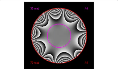
The phase plate was then calculated from the aberra-tion coefficients of the last measured probe tableau for different outer tilt angles of the optical axis. Figure 2 shows the phase plate used to visualize the corrected aberration coefficients. Here, the defocus C1 and
two-fold astigmatismA1were neglected. The black color
in-dicates the upper limit towards−π+k2π, while white
[image:3.595.57.541.89.292.2]represents the lower limit towards +π+k2π. where π represents an integer. The phase plate was drawn to the tilt angle at which a limit of 12π was reached (outer cir-cle). The inner circle indicates theπ/4 limit. The radii are displayed in the upper (30 mrad) and lower (70 mrad) left edges, respectively. Together with each radius, the five-order astigmatism aberration coefficient (A4) with
Figure 1Zemlin tableau for measurement of aberration coefficients.
[image:3.595.58.538.423.704.2]the largest contribution at this radius is given on the right. The phase shift image (phase plate) was calculated from the measured aberrations for the DCOR. The ap-proximate size of the corrected area is indicated by the 30-mrad (half angle) aperture.
For aberration correction, improvement in the transfer function was directly seen in the ronchigram, a diffrac-tion pattern of an amorphous film obtained using a large convergence angle that gives a direct image of the aber-ration function χ(θ, φ). In the present aberration cor-rected system, there was a large uniform region at the
center of the ronchigram. The range of minimum con-trast at the center defined an area of constant electron phase that was appropriate for use in forming a small probe. By allowing higher convergence angles, the beam intensity also increased, which is important for chemical analysis.
HRTEM characterization
[image:4.595.57.291.87.319.2]The HRTEM image revealed that the interplanar spacing of the silicon (111) planes observed along the [110] zone axis was approximately 0.313 nm (Figure 3). The atomic
Figure 3HRTEM image of the SiGe/Si interface.
[image:4.595.308.539.88.313.2]Figure 4HRSTEM HAADF image (Zcontrast) of a 10-nm-thick SiGe epitaxial layer with the SiGe/Si interface.
Figure 5HRSTEM HAADF image of the dumbbell SiGe/Si interface.
Figure 6FFT result showing information transfer to 0.78 Å.
Hsiaoet al. Nanoscale Research Letters2014,9:578 Page 4 of 7
[image:4.595.58.287.485.708.2] [image:4.595.303.539.500.711.2]structure of the SiGe/Si interface was not apparent, how-ever, and thus, the SiGe/Si interface could not be iden-tified using the phase contrast image formation. While the bright point indicated the intersection of the lattice fringes, the accurate position of the atomic column could not be determined.
HRSTEM characterization
The HRSTEM analysis with a large coherent convergent beam provided incoherent atomic resolved images on a
[image:5.595.58.538.89.342.2]low-order zone axis through thermal diffuse scattering (TDS). In the high-resolution HAADF images, unlike for the HRTEM images, the projected atomic columns were identified by bright spots independent of the defocus of the probe-forming lens and the sample thickness, except for the unsuitable defocus values. In addition, the in-coherent images displayed a contrast that was strongly dependent on the atomic number (Z contrast). Figure 4 presents the HAADF image of a 10-nm-thick SiGe epita-xial layer with an interface composed of a silicon crystal
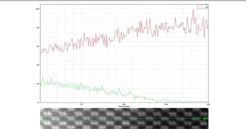
Figure 7Reference atomic resolution SiGe/Si interface HRSTEM HAADF image along the [110] direction.With the corresponding EDS line scans for Si and Ge (red and green lines, respectively).
[image:5.595.57.541.518.715.2]connected coherently to the superlattice of the SiGe layer. As can be seen in the figure, the contrast for the Si and SiGe atoms was clearer at the interface. Furthermore, the absence of the Fresnel interference effect and the high sensitivity to the tilting of the crystal made it easy to per-form structural and compositional analyses at the inter-face and the surinter-face region with atomic-scale resolution. Due to these advantages, the HAADF method is widely used for the analysis of boundary structures and for the distribution analysis of dopants in materials.
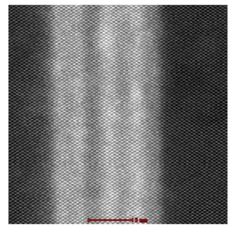
The resolution of such HRSTEM images can be deter-mined using the criterion separation of the atom peaks in the image. Evaluation of the resolution using this criter-ion requires a specimen that can be tilted at an orientatcriter-ion in which the atoms are separated by a known distance. Figure 5 shows the HRSTEM dumbbell image of the SiGe/Si interface in the [110] orientation, and Figure 6 shows the fast Fourier transform (FFT) indicating a re-solution of 0.78 Å (point rere-solution). The distance be-tween the separated dumbbell Si and Ge atoms was approximately 1.36 Å. Models for silicon in the [112n] orientation show typical ‘dumbbell’ arrangements. In-creasing the value of n from 0 to 3 moved the atoms closer together in the projection, and the projected atom-atom spacing in the silicon changed from 1.36 Å for the [110] orientation to 0.31 Å for the [116] orientation [16].
EDS analysis
Figure 7 presents the atomic resolution SiGe/Si interface HAADF image along the [110] plane with the simulta-neously recorded EDS line scans (Si: red line, Ge: green line). The inelastic interaction of x-ray was effectively local, as was observed in the HRSTEM HAADF image, and the inner-shell ionization potential was as localized as possible for a given ionization edge. Consequently, it was possible to directly correlate the resulting incoher-ent HAADF image to the EDS line scan signals [15]. The interfacial layer contained a few atomic percent of Ge, the atoms of which had been diffused from crystal-line SiGe nanolaminates. The EDS spectrum for Si and Ge is shown in Figure 8. The Ge line scan (green) was constructed from the sum of the Ge K- and L-shell ionization events. The corresponding Si line scan (red), however, was constructed using only the Si K shell. The detectors had count rates an order of magnitude greater than conventional detectors, and thus, the signal-to-noise ratio was improved.
Conclusions
The atomic resolution imaging and spectroscopic analysis of an SiGe/Si interface grown via molecular beam epitaxy was investigated using aberration-corrected HRSTEM. The phase plates were calculated from the aberration
coefficients of the measured probe tableau for various outer tilt angle of the optical axis, and the accuracy re-quired for the compensation of the various residual aber-ration coefficients in order to achieve sub-angstrom resolution with the electron optics system was evaluated. The HRSTEM HAADF dumbbell image revealed that the distance between the Si and Ge atoms was approximately 1.36 Å, and the corresponding fast Fourier transform con-firmed a point resolution on the sub-angstrom scale (0.78 Å). In addition, the experimental results demon-strated that complementary EDS line scan signals could be directly correlated to the atomic-resolution HAADF image.
Competing interests
The authors declare that they have no competing interests.
Authors’contributions
CNH and SYK designed the experiment and measurements. CNH and WCC executed the experiments. CNH and FYL examined the written report. All authors read and approved the final manuscript.
Acknowledgements
The authors gratefully acknowledge financially support from the Ministry of Science and Technology, Taiwan (contract no. 103-2622-E-492 -011 -CC3).
Author details
1Instrument Technology Research Center, National Applied Research
Laboratories, Hsinchu 30076, Taiwan.2Department of Electronic Engineering,
Chang Gung University, Gueishan 33302, Taiwan.3Department of Photonics
Engineering, Yuan Ze University, Taoyuan 32003, Taiwan.
Received: 20 June 2014 Accepted: 8 October 2014 Published: 17 October 2014
References
1. Scherzer O:Über einige Fehler von Elektronenlinsen.Zeitschrift für Physik
1936,101(9):593–603.
2. Scherzer O:Sphärische und chromatische Korrektur von Elektronenlinsen.
Optik1947,2:114–132.
3. Haider M, Uhlemann S, Schwan E, Rose H, Kabius B, Urban K:Electron microscopy image enhanced.Nature1998,392:768–769.
4. Uhlemann S, Haider M:Residual wave aberrations in the first spherical aberration corrected transmission electron microscope.Ultramicroscopy
1998,72:109–119.
5. Krivanek OL, Dellby N, Lupini AR:Towards sub-Å electron beams.
Ultramicroscopy1999,78:1–11.
6. Haider M, Uhlemann S, Zach J:Upper limits for the residual aberrations of a high-resolution aberration-corrected STEM.Ultramicroscopy2000,
81:163–175.
7. Batson PE, Dellby N, Krivanek OL:Sub-angstrom resolution using aberration-corrected electron optics.Nature2000,418:617–620. 8. Nellist PD, Chisholm MF, Dellby N, Krivanek OL, Murfitt MF, Szilagyi ZS,
Lupini AR, Borisevich A, Sides WH Jr, Pennycook SJ:Direct sub-angstrom imaging of a crystal lattice.Science2004,305:1741–1741.
9. Midgley PA, EDunin-Borkowski R:Electron tomography and holography in materials science.Nature Mater2009,8:271–280.
10. Van Aert S, Batenburg KJ, Rossell MD, Erni R, van Tendeloo G:Three dimensional atomic imaging of crystalline nanoparticles.Nature2011,
470:374–377.
11. Chen CC, Zhu C, White ER, Chiu CY, Scott MC, Regan BC, Marks LD, Huang Y, Miao J:Three-dimensional imaging of dislocations in a nanoparticle at atomic resolution.Nature2013,496:74–77.
12. Urban KW:Studying atomic structures by aberration-corrected transmission electron microscopy.Science2008,321:506–510.
13. Muller D:Structure and bonding at the atomic scale by scanning transmission electron microscopy.Nat Mater2009,8:263–270.
Hsiaoet al. Nanoscale Research Letters2014,9:578 Page 6 of 7
14. Chu M-W, Liou SC, Chang C-P, Choa F-S, Chen CH:Emergent chemical mapping at atomic-column resolution by energy-dispersive X-ray spectroscopy in an aberration-corrected electron microscope.Phys Rev
Lett2010,104:196101–196104.
15. D’Alfonso AJ, Freitag B, Klenov D, Allen LJ:Atomic-resolution chemical mapping using energy-dispersive x-ray spectroscopy.Phys Rev B2010,
81:100101. 1–4.
16. O'Keefe MA:Seeing atoms with aberration-corrected sub-angstrom electron microscopy.Ultramicroscopy2008,108:196–209.
doi:10.1186/1556-276X-9-578
Cite this article as:Hsiaoet al.:Interfacial atomic structure analysis at sub-angstrom resolution using aberration-corrected STEM.Nanoscale
Research Letters20149:578.
Submit your manuscript to a
journal and benefi t from:
7 Convenient online submission
7 Rigorous peer review
7 Immediate publication on acceptance
7 Open access: articles freely available online
7 High visibility within the fi eld
7 Retaining the copyright to your article