International Journal of Emerging Technology and Advanced Engineering
Website: www.ijetae.com (ISSN 2250-2459,ISO 9001:2008 Certified Journal, Volume 5, Issue 8, August 2015)
260
“To Reduces the Static and Dynamic Power Dissipation
through Variable Body Biasing Technique”
Arpit Chourgade
1, Sachin Bandewar
2 1Student, 2Asst. Prof. & HOD, RKDF UniversityAbstract— In deep sub micron technology, A key for a low power design is leakage power. Power dissipation is an important consideration in the design of CMOS VLSI circuits. Higher power consumption leads to decrease in battery life in case of battery powered applications and affects reliability packaging and cooling costs. Now we introduced a technique called Variable Body Biasing for designing CMOS gates which significantly cuts down the leakage current without increasing the dynamic power dissipation. Variable Body Biasing is a technique that tackle the leakage problem in CMOS circuits, which uses single additional leakage control transistor, driven by the output from the pull up and pull down networks, which is placed in a path from pull down network to ground which provides the additional resistance thereby reducing the leakage current in the path from supply to ground. The main advantage of this techniques is that Variable Body Biasing technique does not require any additional control and monitoring circuitry, thereby limits the area and also decreases the power dissipation in active state. Along with this, the other advantage with Variable Body Biasing technique is that it decreased the leakage power which is more efficient in aspects of area and power dissipation compared to other leakage power reduction techniques.
I. INTRODUCTION
To reduce the leakage current in the sleep mode we ensured that the body to source voltage of the sleep transistor is increased. To do that we added a PMOS(M2) and a NMOS (M5) in the previouly discussed sleepy keeper circuit (Fig.6). During sleep mode PMOS (M2) is OFF so the body to source voltage of the pull up PMOS (M1) is higher than in the active mode. For a turned off single transistor leakage current (Isub0) can be expressed as follows:
Isub0 = A
)
Where, A= µ0 C0x (W/Leff) ; n is the
sub-threshold
swing coefficient, and Vθ is the thermal voltage. Vgs0,
Vth0, Vsb0 and Vds0 are the gate-to-source voltage, the zero-bias threshold voltage, the base-to-source voltage and the drain-to-source voltage, respectively, γ is the body-bias effect coefficient, and η is the Drain Induced Barrier Lowering (DIBL) coefficient, μ is zero-bias mobility, Cox is the gate-oxide capacitance, W is the width of the transistor, and Leff is the effective channel length [8].
From equation (1) we see that leakage current (Isub0) decreases as Vsb0 increases. As a result of Body effect,
Vth alsoincreases which lowers the performance. During the active mode, the performance is improved as the PMOS (M2) is ON which makes the Vth of the pull up PMOS (M1) lower again.
The same discussion is applicable for the pull down NMOS (M4) and NMOS (M5). The remaining NMOS (M3) and PMOS (M6) works together for retaining the state in the sleep mode. If the output is high, in the sleep mode, the NMOS (M3) will keep the output high. Similarly, the PMOS (M6) will maintain the state in sleep mode if the output is low.
II. PREVIOUS APPROACHES
In this section we discussed the previous approaches which are nearly related to our research. Here we analyse previous low power technique that primarily target for reducing leakage. These techniques for leakage reduction can be grouped into two categories: (i) State saving (ii) state destructive [5]. State save can have an advantage over the state destructive. The approaches that are adopted in VLSI design. We here review previously proposed circuit level approaches for sub-threshold leakage power reduction.
2.1 Sleep Transistor Approach
International Journal of Emerging Technology and Advanced Engineering
Website: www.ijetae.com (ISSN 2250-2459,ISO 9001:2008 Certified Journal, Volume 5, Issue 8, August 2015)
[image:2.595.57.274.112.373.2]261
Figure 2.1 Sleep Approach2.2 Sleepy Stack Approach
[image:2.595.317.546.250.495.2]The sleepy stack approach combines the sleep and stack approaches [3] [4] (Figure 2.2). The sleepy stack technique divides existing transistors into two half size transistors like the stack approach. Then sleep transistors are added in parallel to one of the divided transistors. During sleep mode, sleep transistors are turned off and stacked transistors suppress leakage current while saving state. Area penalty is a significant matter for this approach since every transistor is replaced by three transistors.
Figure 2.2 Sleepy Stack
2.3 Sleepy Keeper Approach
[image:2.595.53.273.513.748.2]Sleepy keeper utilizes leakage feedback technique [5] (Figure 2.3). In this approach, a PMOS transistor is placed in parallel to the sleep transistor (S) and a NMOS transistor is placed in parallel to the sleep transistor (S'). The two transistors are driven by the output of the inverter. During sleep mode, sleep transistors are turned off and one of the transistors in parallel to the sleep transistors keep the connection with the appropriate power rail.
Figure 2.3 Sleepy Keeper 2.4 Dual Sleep Approach
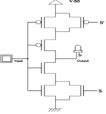
Dual sleep approach [6] (Figure 2.4) uses the advantage of using the two extra pull-up and two extra pull-down transistors in sleep mode either in OFF state or in ON state. Since the dual sleep portion can be made common to all logic circuitry, less number of transistors is needed to apply a certain logic circuit.
[image:2.595.323.561.573.762.2]International Journal of Emerging Technology and Advanced Engineering
Website: www.ijetae.com (ISSN 2250-2459,ISO 9001:2008 Certified Journal, Volume 5, Issue 8, August 2015)
262
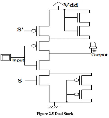
2.5 Dual Stack Approach [image:3.595.52.274.219.458.2]In dual stack approach [7] (Figure 2.5), 2 PMOS in the pull down network and 2 NMOS in the pull-up network are used. The advantage is that NMOS degrades the high logic level while PMOS degrades the low logic level. Compared to previous approaches it requires greater area. The delay is also increased.
Figure 2.5 Dual Stack
III. PRAPOSED MATHEDOLOGY
In this section, we introduce our new leakage power reduction techniques. At first we will discuss the structure of the techniques then we will show the operations of these techniques.
3.1 Variable Body Biasing Approach
To reduce the leakage current in the sleep mode we ensured that the body to source voltage of the sleep transistor is increased. To do that we added a PMOS(M2) and a NMOS (M5) in the previouly discussed sleepy keeper circuit (Fig.6). During sleep mode PMOS (M2) is OFF so the body to source voltage of the pull up PMOS (M1) is higher than in the active mode. For a turned off single transistor leakage current (Isub0) can be expressed as follows:
Isub0 = A
)
Where, A= µ0 C0x (W/Leff) ; n is the
sub-threshold
Swing coefficient, and Vθ is the thermal voltage. Vgs0,
Vth0, Vsb0 and Vds0 are the gate-to-source voltage, the zero-bias threshold voltage, the base-to-source voltage and the drain-to-source voltage, respectively, γ is the body-bias effect coefficient, and η is the Drain Induced Barrier Lowering (DIBL) coefficient, μ is zero-bias mobility, Cox is the gate-oxide capacitance, W is the width of the transistor, and Leff is the effective channel length [8]. From equation (1) we see that leakage current (Isub0)decreases as Vsb0 increases. As a result of Body effect, Vth alsoincreases which lowers the performance. During the active mode, the performance is improved as the PMOS (M2) is ON which makes the Vth of the pull up PMOS (M1) lower again.
The same discussion is applicable for the pull down NMOS (M4) and NMOS (M5). The remaining NMOS (M3) and PMOS (M6) works together for retaining the state in the sleep mode. If the output is high, in the sleep mode, the NMOS (M3) will keep the output high. Similarly, the PMOS (M6) will maintain the state in sleep mode if the output is low.
[image:3.595.322.564.403.683.2]3.1.1 Structure of variable body biasing technique
International Journal of Emerging Technology and Advanced Engineering
Website: www.ijetae.com (ISSN 2250-2459,ISO 9001:2008 Certified Journal, Volume 5, Issue 8, August 2015)
263
This technique in figure 3.1.1 uses two parallel connected sleep transistors in Vdd and two parallel connected sleep transistors in GND. The source of one of the pmos sleep transistor is connected to the body of other pmos sleep transistor for having so called body biasing effect. Similarly the source of one of the nmos sleep transistor is connected to the body of other nmos sleep transistor for having the same effect as for pmos sleep transistors. So, leakage reduction in this technique occurs in two ways.
Firstly, the sleep transistor effect and secondly, the variable body biasing effect. It is well known that pmos transistors are not efficient at passing GND; similarly,it is well known that nmos transistors are not efficient at passing Vdd. But this variable body biasing technique uses pmos transistor in GND and nmos transistor in Vdd, both are in paralleled to the sleep transistors, for maintaining exact logic state during sleep mode. This technique uses aspect ratio W/L=3 for nmos transistor and W/L=6 for pmos transistor in the main inverter portion. For the sleep transistors this technique uses aspect ratio W/L=1 for both the nmos and pmos transistors. The extra two transistors of the design for maintaining the logic state during sleep mode also use aspect ratio W/L=1. Due to the minimum aspect ratio the sub-threshold current reduces.
3.2 Operation of Variable body biasing technique
During active mode S=1 and S'=0 is asserted. Then the entire sleep transistors are ON and the inverter is in active mode. For different input signal desired output signal is caught. During sleep mode or inactive mode S=0 and S'=1 is asserted. Then the entire sleep transistor is turned OFF. Since the sources of the nmos and pmos sleep transistors are connected to the body of similar transistor, the threshold voltage of the sleep transistors increases due to the body biasing effect [17] during sleep mode.
This increase of threshold voltage of the transistors reduces the leakage current. That's why the static power consumption is also lowers. This variable body biasing technique also has two extra transistors in parallel to the sleep transistors. The purpose of this extra transistor is to save data during inactive mode of the circuit.
Let us to save the value '1' in sleep mode. Assume that the '1' value has already been calculated. This technique uses this output value of '1' and an nmos transistor connected to Vdd to maintain output value equal to '1' when in sleep mode. When in sleep mode this nmos transistor is the only source of Vdd to the pull up network since the sleep transistors are turned off.
Similarly to maintain a value of '0' in sleep mode, assume that the '0' value has already been calculated, this technique uses this output value of '0' and a pmos transistor connected to GND to maintain output value equal to '0' when in sleep mode. When in sleep mode, this pmos transistor is the only source of GND to the pull down network since the sleep transistors are turned off.
IV. SIMULATION RESULTS
We compare the stacked sleep approach, variable body biasing technique and forced sleep technique to a base case and five other previous approaches, namely sleep transistor, forced stack, sleepy stack, sleepy keeper and dual sleep. Thus, we compare nine design approaches in terms of power consumption (dynamic and static), delay and area. To show that the approaches are applicable to general logic design, we choose a chain of four inverters. We use Synopsis HSPICE [18] for simulation purpose to estimate delay and power consumption. Area is calculated with the help of MICROWIND. All considered approaches are evaluated for performance by using a single, low-Vth for all transistors. The inverter chain uses three inverters each with W/L=6 for PMOS and W/L=3 for NMOS for the base case. For example, sleep transistors (Figure 3.2) used in the pull-up and pull-down networks of the base case inverter chain have W/L=6 and W/L=3, respectively. Transistors in the forced stack approach (Figure 3.3) are sized to half of the size of the base case transistors, e.g., transistors used in pull-up and pull-down of the base case inverter chain have W/L=3 and W/L=1.5, respectively.
International Journal of Emerging Technology and Advanced Engineering
Website: www.ijetae.com (ISSN 2250-2459,ISO 9001:2008 Certified Journal, Volume 5, Issue 8, August 2015)
264
Table 1:Power supply voltage for different technologies
180n 130n 90n 65n 45n 32n 22n
1.8V 1.3V 1.2V 1.1V 1.0V 0.9V 0.8V
[image:5.595.318.541.220.432.2]4.1 Simulation results for a chain of four inverters
[image:5.595.45.292.274.741.2]Table 2 shows the result of different methods using 32 nm technologies.
Table 2: Data for 32 nm technology
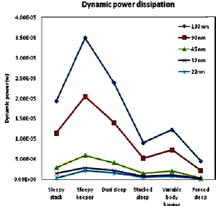
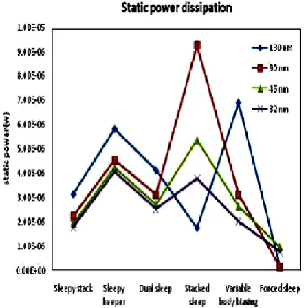
Figure 4.1(a) shows the static power dissipation of a chain of four inverters in different technologies. In case of 32 nm technology stacked sleep approach gives 83.41% and variable body biasing technique gives 69.29% good results than the dual sleep approach. The forced sleep approach shows a 99.49% satisfactory result rather than the dual sleep approach.
Figure 4.1(b) shows the dynamic power dissipation of a chain of four inverters in different technologies. In case of 32 nm technology stacked sleep approach gives 65.49% and variable body biasing technique gives 50.44% good results than the dual sleep approach. Forced sleep approach also shows a 93.53% good result than the dual sleep approach.
4.2 Simulation Results For SRAM Cell
[image:5.595.325.554.578.768.2]The simulation result for SRAM cell with 32 nm technology is given below in tabulated form.
Table 3: Data for 32 nm technology: Method Static power
(w)
Dynamic power
Sleepy stack 7.05E-10 1.45E-06
Sleepy keeper 1.50E-09 2.85E-06
Dual sleep 1.02E-04 2.09E-06
Stacked sleep 1.96E-10 7.20E-07
Variable body
biasing 3.64E-10 1.03E-06
Forced sleep 5.99E-12 1.35E-03
Method Static
power (w)
Dynamic power
Sleepy stack 1.75E-06 2.94E-05
Sleepy keeper 4.04E-06 5.81E-05
Dual sleep 2.52E-06 2.24E-05
Stacked sleep 3.78E-06 1.22E-06
Variable body
biasing 2.00E-06 1.98E-06
International Journal of Emerging Technology and Advanced Engineering
Website: www.ijetae.com (ISSN 2250-2459,ISO 9001:2008 Certified Journal, Volume 5, Issue 8, August 2015)
265
Figure 4.2(a) shows the static power dissipation of an SRAM cell in different technologies. In case of 32 nm technology stacked sleep approach gives -49.59% worst and variable body biasing technique gives 20.69% good results than the dual sleep approach. The forced sleep approach shows a 70.08% satisfactory result rather than the dual sleep method.
Figure 4.2(b) shows the dynamic power dissipation of an SRAM cell in different technologies. In case of 32 nm technology stacked sleep approach gives 97.11% and variable body biasing technique gives 95.33% good results than the dual sleep approach.
V. CONCLUSION
In case, a chain of four inverters, Variable body biasing technique, sleepy stack method shows 87.6638% & 42.7778% degraded performance in static power and dynamic power respectively. When compared to sleepy stack method shows 92.8275%, 58.8095% degraded performance than stacked sleep method in dynamic power and static power, respectively. Again In comparison with stacked sleep, dual sleep approach shows 582.81%, 195.96% improved performance in static and dynamic power respectively.
Variable body bias technique 283.66% and 114.240% improved performance in static and dynamic power respectively. Forced sleep technique also gives good performance in static and dynamic power. So the novel stacked sleep, variable body bias and forced sleep technique shows better performance when compared to the sleepy stack and dual sleep method. Finally, these proposed methods show the least speed power product among all methods. Moreover, the novel stacked sleep, variable body bias and forced sleep method shows best performance as far as area requirement and speed are concerned.
REFERENCES
[1] CHANDRAKASAN, A. P., SHENG, S., and BRODERSEN, R. W., "Low- Power CMOS Digital Design," IEEE Journal of Solid-State Circuits, vol. 27, no. 4, pp. 473-484, April 1992.
[2] S. Mutoh et al., "1-V Power Supply High-speed Digital Circuit Technology with Multithreshold-Voltage CMOS," IEEE Journal of Solis-State Circuits, Vol. 30, No. 8, pp. 847-854, August 1995. [3] Q. Wang and S. Vrudhula, “Static power optimization of deep
sub-micron CMOS circuits for dual VT technology,” in Proc. ICCAD, Apr. 1998, pp. 490–496.
[4] L. Wei, Z. Chen, M. Johnson, and K. Roy, “Design and optmization of low voltage high performance dual threshold CMOS circuits,” in Proc. 35th DAC, 1998, pp. 489–492. [5] NOSE, K. and SAKURAI, T., "Analysis and Future Trend of
Short-Circuit Power," IEEE Transactions on Computer-Aided Design of Integrated Circuits and Systems, vol. 19, no. 9, pp. 1023-1030, September 2000.
[6] M. D. Powell, S. H. Yang, B. Falsafi, K. Roy, and T. N. Vijaykumar, “Gated-Vdd: A ciruit technique to reduce leakage in deep submicron cache memories,” in Proc. IEEE ISLPED, 2000, pp. 90-95.
[7] NARENDRA, S., S. BORKAR, V. D., ANTONIADIS, D., and CHANDRAKASAN,A., "Scaling of Stack Effect and its Application for Leakage Reduction," Proceedings of 148 the International Symposium on Low Power Electronics and Design, pp. 195-200, August 2001.
[8] J. Kao and A. Chandrakasan, "MTCMOS sequential circuits, Proceedings of European Solid-Stat Circuits Conference, pp 332-335, September 2001.
[image:6.595.53.276.134.359.2] [image:6.595.51.277.458.654.2]International Journal of Emerging Technology and Advanced Engineering
Website: www.ijetae.com (ISSN 2250-2459,ISO 9001:2008 Certified Journal, Volume 5, Issue 8, August 2015)
266
[10] JOHNSON, M., SOMASEKHAR, D., CHIOU, L.-Y., and ROY, K., "Leakage Control with Efficient Use of Transistor Stacks in Single Threshold CMOS," IEEE Transactions on VLSI Systems, vol. 10, no. 1, pp. 1-5, February 2002.
[11] KIM, C. and ROY, K., "Dynamic Vt SRAM: a Leakage Tolerant Cache Memory for Low Voltage Microprocessors," Proceedings of the International Symposium on Low Power Electronics and Design, pp. 251-254, August 2002.
[12] KIM, N., AUSTIN, T., BAAUW, D., MUDGE, T., FLAUTNER, K., HU,J., IRWIN, M., KANDEMIR, M., and NARAYANAN, V., "Leakage Current: Moore's Law Meets Static Power," IEEE Computer, vol. 36, pp. 68-75, December 2003.
[13] H. Narender and R. Nagarajan, “LECTOR: A technique for leakage reduction in CMOS circuits”, IEEE trans. On VLSI systems, vol. 12, no. 2, Feb. 2004.
[14] J.C. Park, V. J. Mooney III and P. Pfeiffenberger, "Sleepy Stack Reduction of Leakage Power," Proceeding of the International Workshop on Power and TimingModeling, Optimization and Simulation, pp. 148-158, September 2004.
[15] J. C. Park, “Sleepy Stack: A new approach to Low Power VLSI logic and memory,” Ph.D. Dissertation, School of Electrical and Computer Engineering, Georgia Institute of Technology, 2005.
[16] J. Park, "Sleepy Stack: a New Approach to Low Power VLSI and Memory," Ph.D. Dissertation, School of Electrical and Computer Engineering, Georgia Institute of Technology, 2005. [Online]. [17] S. H. Kim and V. J. Mooney, “Sleepy Keeper: a new approach to
low-leakage power VLSI design,” IFIP, pp. 367-372, 2006. [18] Se Hun Kim, V.J. Mooney, "Sleepy Keeper: a New Approach to
Low-leakage Power VLSI Design" Proceeding of the 2006 IFIP International Conference on Very Large Scale Integration, pp367-372, Oct. 2006.
[19] B. S. Deepak subramanyan, A. Nunez, “Analysis of subthreshold leakage reduction in CMOS digital circuits,” in Proc. 13th NASA VLSI Symp.,June 2007.
[20] Nittaranjan Karmakar, Mehdi Z. Sadi, Md. Khorshed Alam and M. S. Islam1, "A Novel Dual Sleep Approach to Low Leakage and Area Efficient VLSI Design" IEEE-RSM Proc. 2009, Kota Bahru, Malaysia
[21] P. Verma, R. A. Mishra, “Leakage power and delay analysis of LECTOR based CMOS circuits”, Int’l conf. on computer & communication technology ICCCT 2011.